Week 8. Electronics Design
This week we studied electronics design. I was really looking forward to this week as it has been something I want to get into for a long time.
While I am comfortable with soldering and following a schematic, circuits I was completely new to.
Let's get into it!
Group Project
The group project for this week can be found here
Electronics Design
EDA is electronic design automation, it is software that allows us to design a schematic and circuit.
For our purposes, we are using KiCAD, which is a great open-source EDA allowing both schematic design and PCB design.
I first started by figuring out the parts I wanted in my board, and was inspired by 2020 student Quentin Bolsee, who created a simple pad keyboard using a SAMD21 microcontroller.
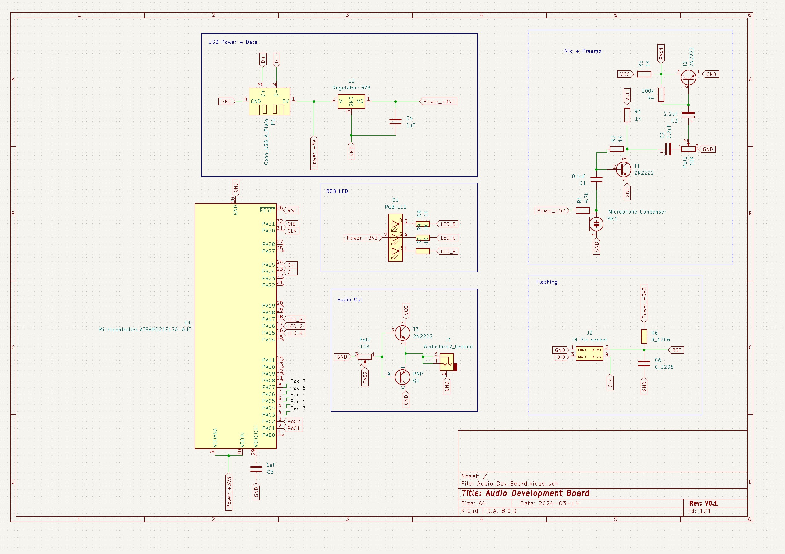 I knew I wanted a few parts :
1. Pads to progam and play a simple tune
2. A RGB LED to give some visual feedback
3. Some analog circuits (a microphone preamp input and headphone amp output)
4. USB capable so I could connect directly to my computer
5. SWD capable to connect to other types of boards as well
6. A compact footprint so I could not go overboard with the size
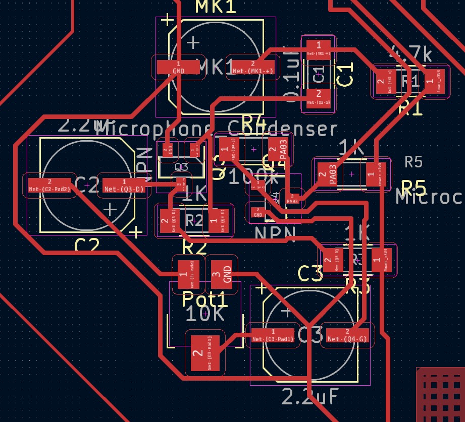
Given all this, I separated each section in the schematics in order to have them well organised.
After having done this, I switched to the PCB view in KiCAD, and started working on organising my compact and well-filled PCB.
After playing around with the software, I produced my V1 PCB design.
I knew I wanted a few parts :
1. Pads to progam and play a simple tune
2. A RGB LED to give some visual feedback
3. Some analog circuits (a microphone preamp input and headphone amp output)
4. USB capable so I could connect directly to my computer
5. SWD capable to connect to other types of boards as well
6. A compact footprint so I could not go overboard with the size
Given all this, I separated each section in the schematics in order to have them well organised.
After having done this, I switched to the PCB view in KiCAD, and started working on organising my compact and well-filled PCB.
After playing around with the software, I produced my V1 PCB design.
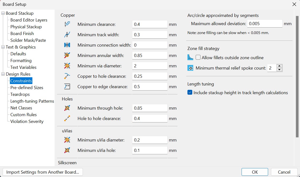
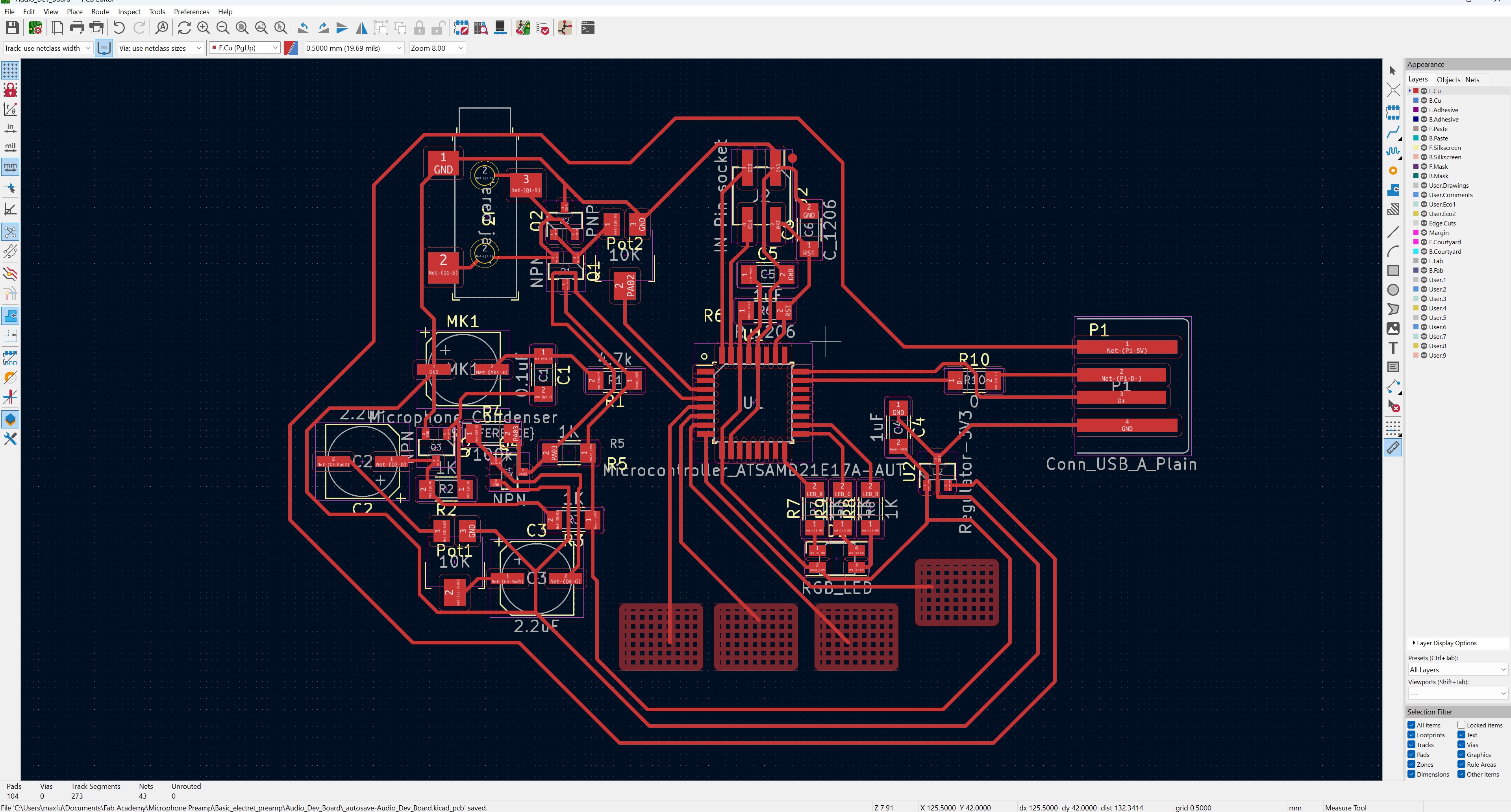 During this design process, we have to use several constraints, to make sure our PCBs can be cut properly on the machine:
1. Make sure the tracks are at least 0.4mm wide (we can go under or over that but 0.4mm is a safe size)
2. Set the spacing between items to be at least 0.4mm due to the size of our smallest endmill between 1/64", or about 0.4mm. If we have smaller spaces, the endmill simply can't go through to cut them.
3. Set the hole size to at least 0.8mm (actually should be 0.82 to be safe), otherwise the 1/32" endmill used to make holes cannot make the correct holes.
This was not idea design for a few reasons:
1. My GND, 3V3, and 5V lines were all running all around the board, causing potential issues if they accidentally touched.
2. The voltage regulator used is too small and does not give an ideal amount of current.
3. After consulting my friend Lennart Bugel who is an audio electronics engineer, my amplifier configuration would not work and would just badly clip the signal. He helped me to redesign it, which gave way to the next design.
During this design process, we have to use several constraints, to make sure our PCBs can be cut properly on the machine:
1. Make sure the tracks are at least 0.4mm wide (we can go under or over that but 0.4mm is a safe size)
2. Set the spacing between items to be at least 0.4mm due to the size of our smallest endmill between 1/64", or about 0.4mm. If we have smaller spaces, the endmill simply can't go through to cut them.
3. Set the hole size to at least 0.8mm (actually should be 0.82 to be safe), otherwise the 1/32" endmill used to make holes cannot make the correct holes.
This was not idea design for a few reasons:
1. My GND, 3V3, and 5V lines were all running all around the board, causing potential issues if they accidentally touched.
2. The voltage regulator used is too small and does not give an ideal amount of current.
3. After consulting my friend Lennart Bugel who is an audio electronics engineer, my amplifier configuration would not work and would just badly clip the signal. He helped me to redesign it, which gave way to the next design.
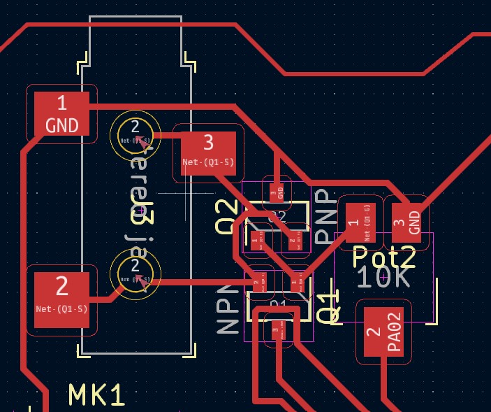
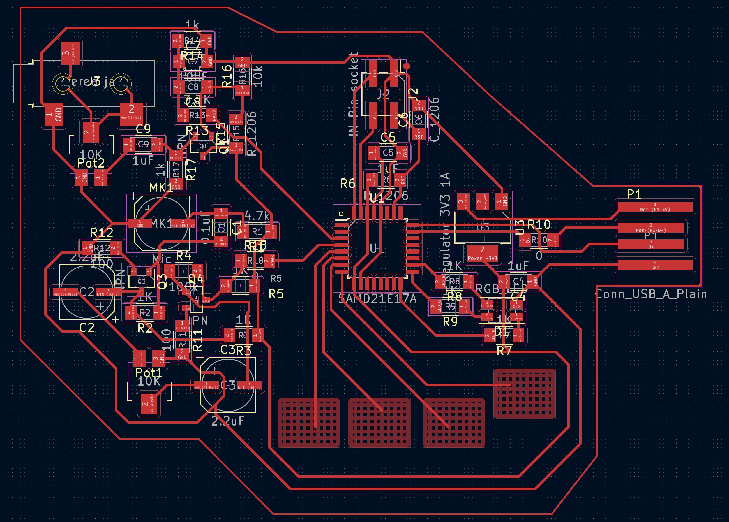 In order to get everything to fit on a single layer, I used two 0 ohm resistors (which work just like little wires) in order to put traces underneath them.
The main differences were in the output section, which went from this :
In order to get everything to fit on a single layer, I used two 0 ohm resistors (which work just like little wires) in order to put traces underneath them.
The main differences were in the output section, which went from this :
 To this :
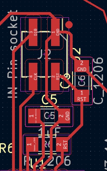
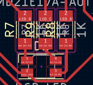
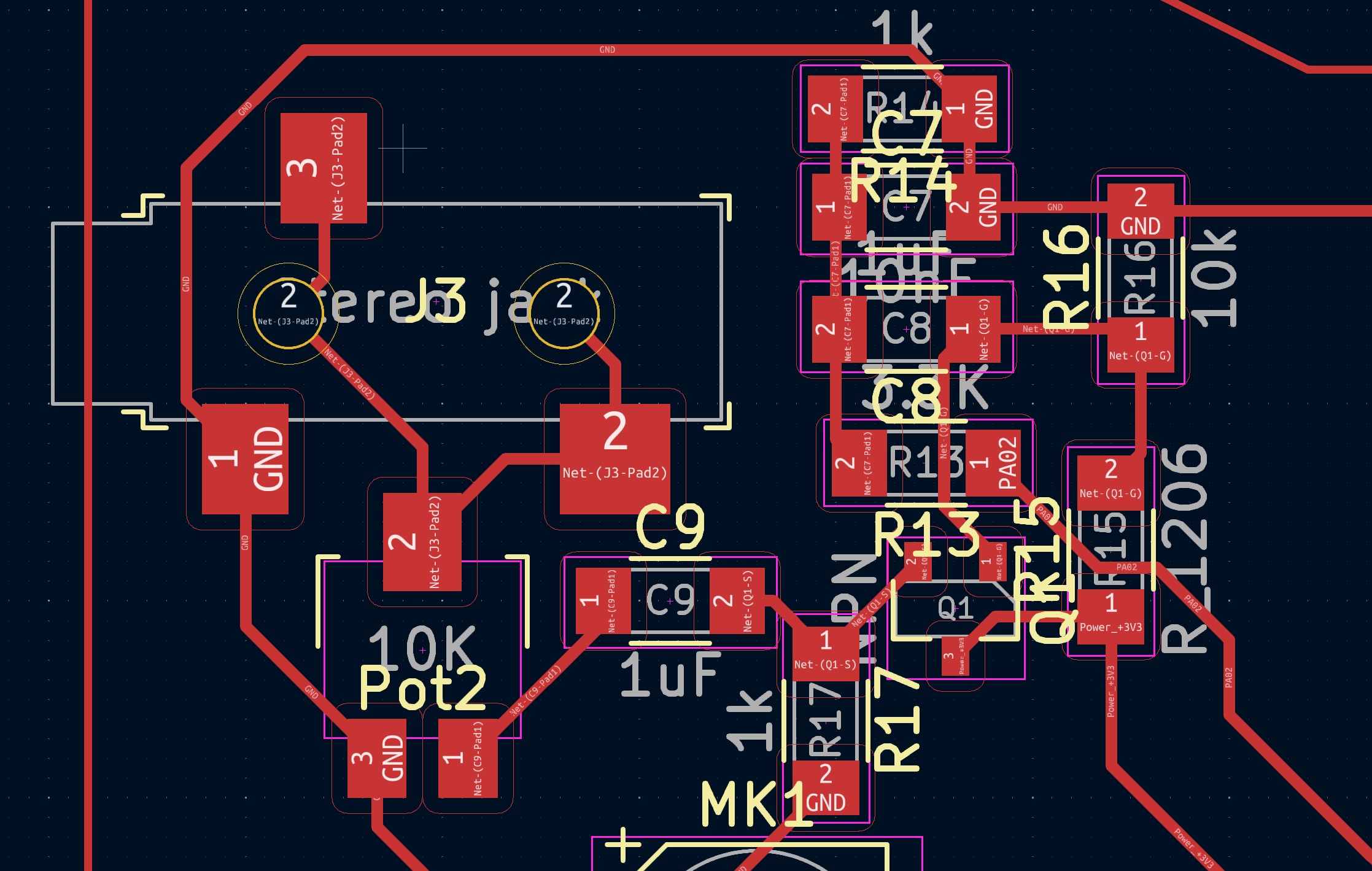 Here is a better view at the different sections on the PCB :
Electronics Design Settings
For the design settings, I had to set a few constraints to make sure my files would be correct for cutting.
PCB Cutting and Soldering
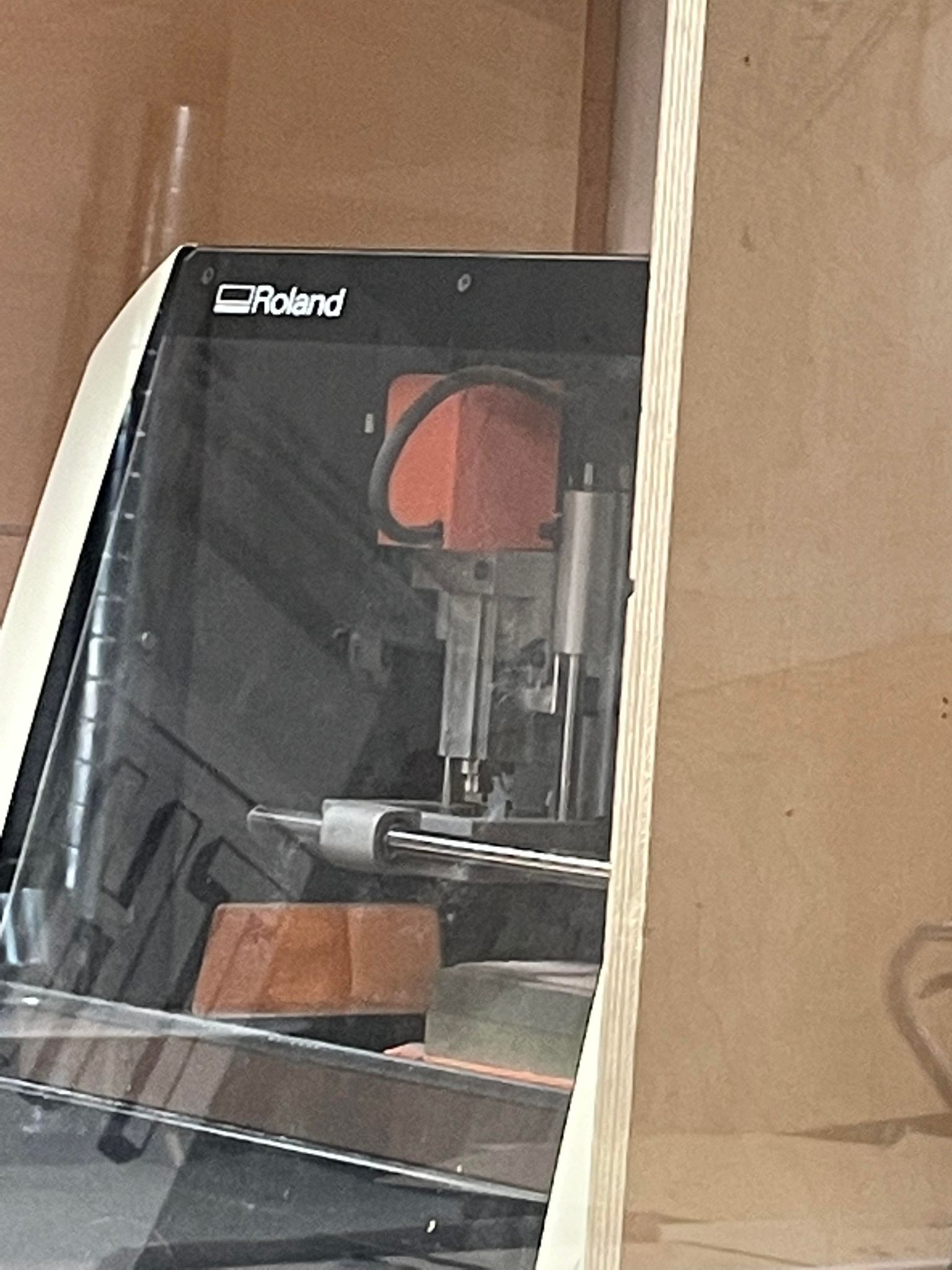
After this, it was finally time to do some cutting and get the PCB on the way! Using our trusty Roland SRM-20
 The first cut, I had made the microcontroller traces too wide, so the Roland simply did not cut through them, and I had to go back over them after, leading to all of them being cut off...
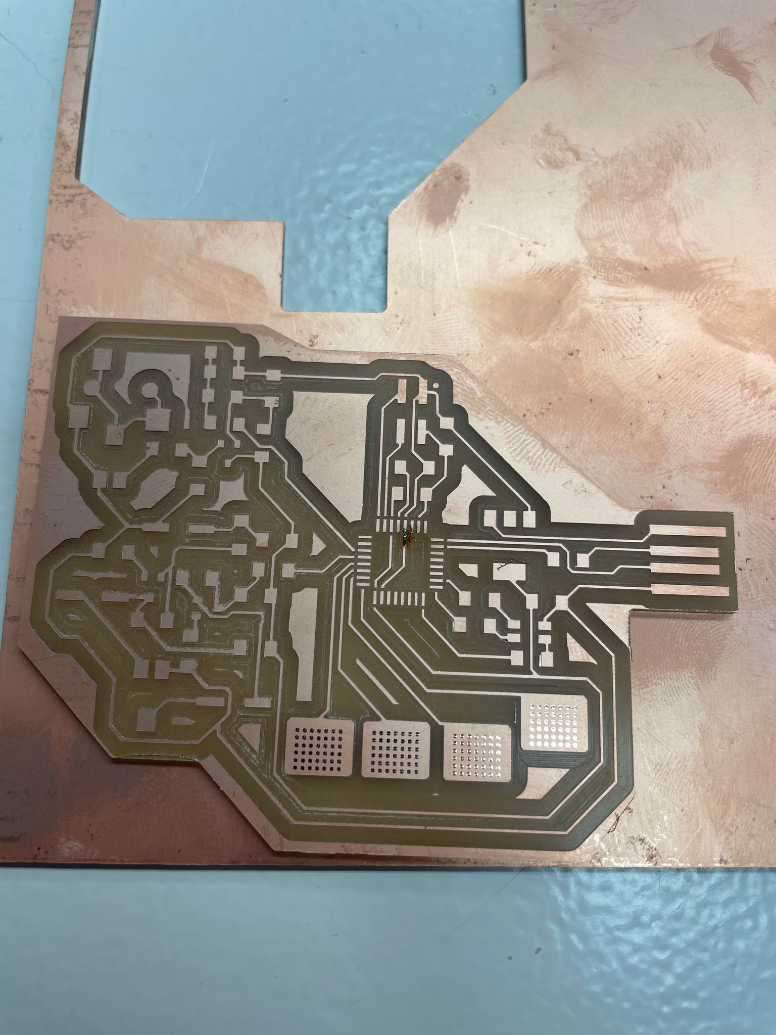 I debated whether to try to connect them with a bit of solder, and after trying to get it clean for a while, I decided to simply cut another board.
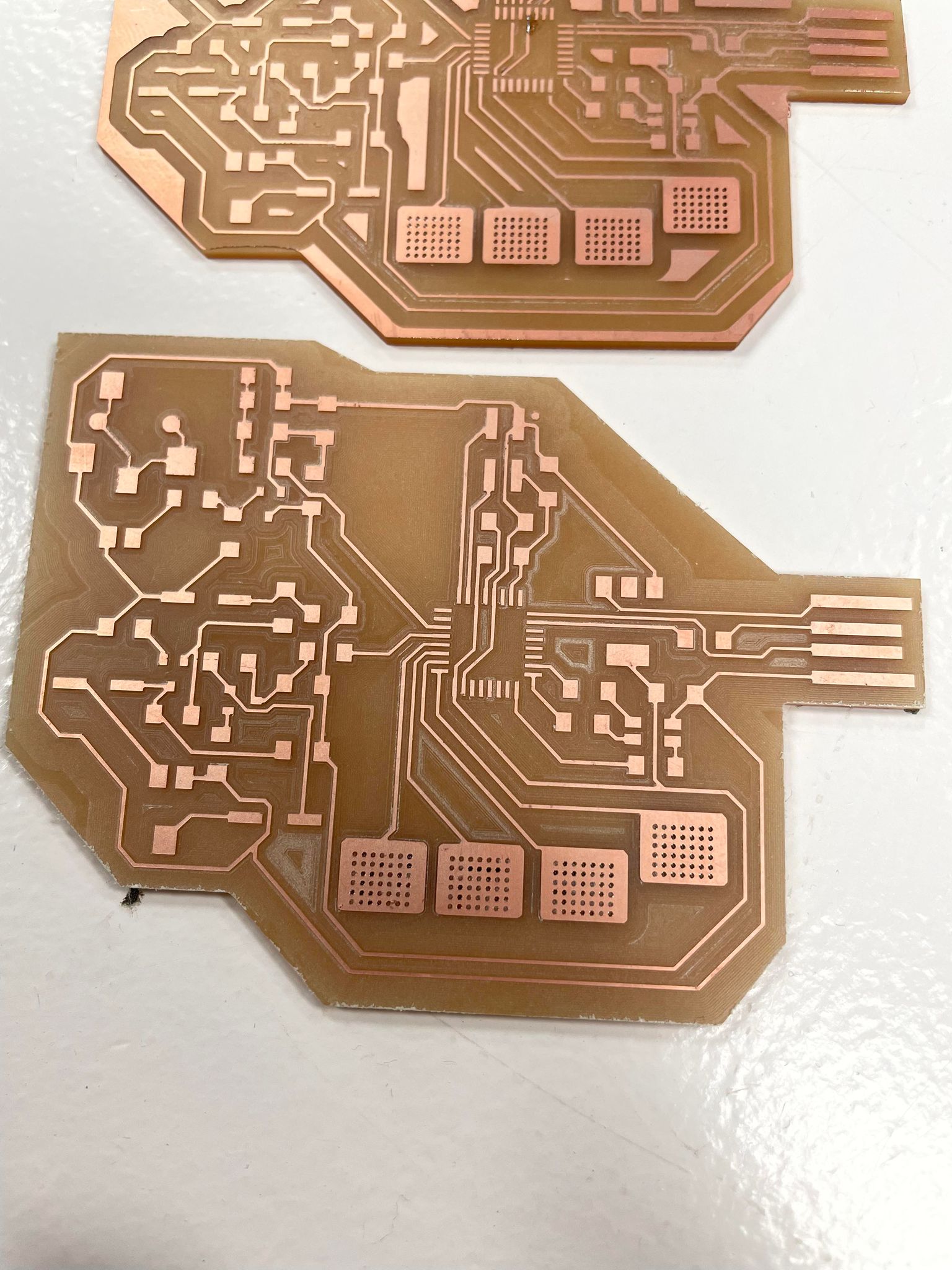 The new board came out very well, and I even spent the time cutting out all excess copper for a very clean look.
I then started soldering my components!
I was very careful and was quite happy with my soldering for most of this part.
The new board came out very well, and I even spent the time cutting out all excess copper for a very clean look.
I then started soldering my components!
I was very careful and was quite happy with my soldering for most of this part.
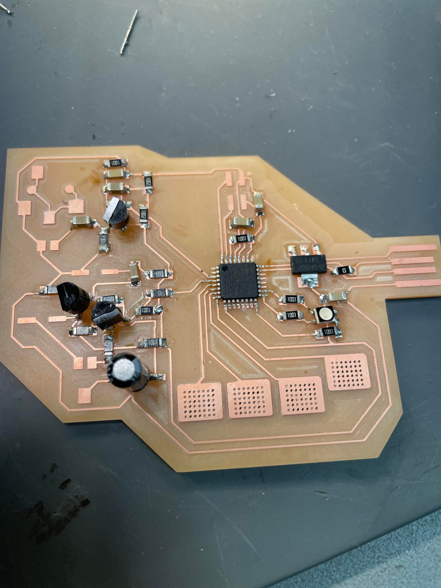 Then I realised some of the footprints in KiCAD were not parts we physically had in stock... Coincidentally, the biggest parts, output jack and both potentiometers were simply not correct.
I grabbed some bigger parts and did my best to make them fit.
Then I realised some of the footprints in KiCAD were not parts we physically had in stock... Coincidentally, the biggest parts, output jack and both potentiometers were simply not correct.
I grabbed some bigger parts and did my best to make them fit.
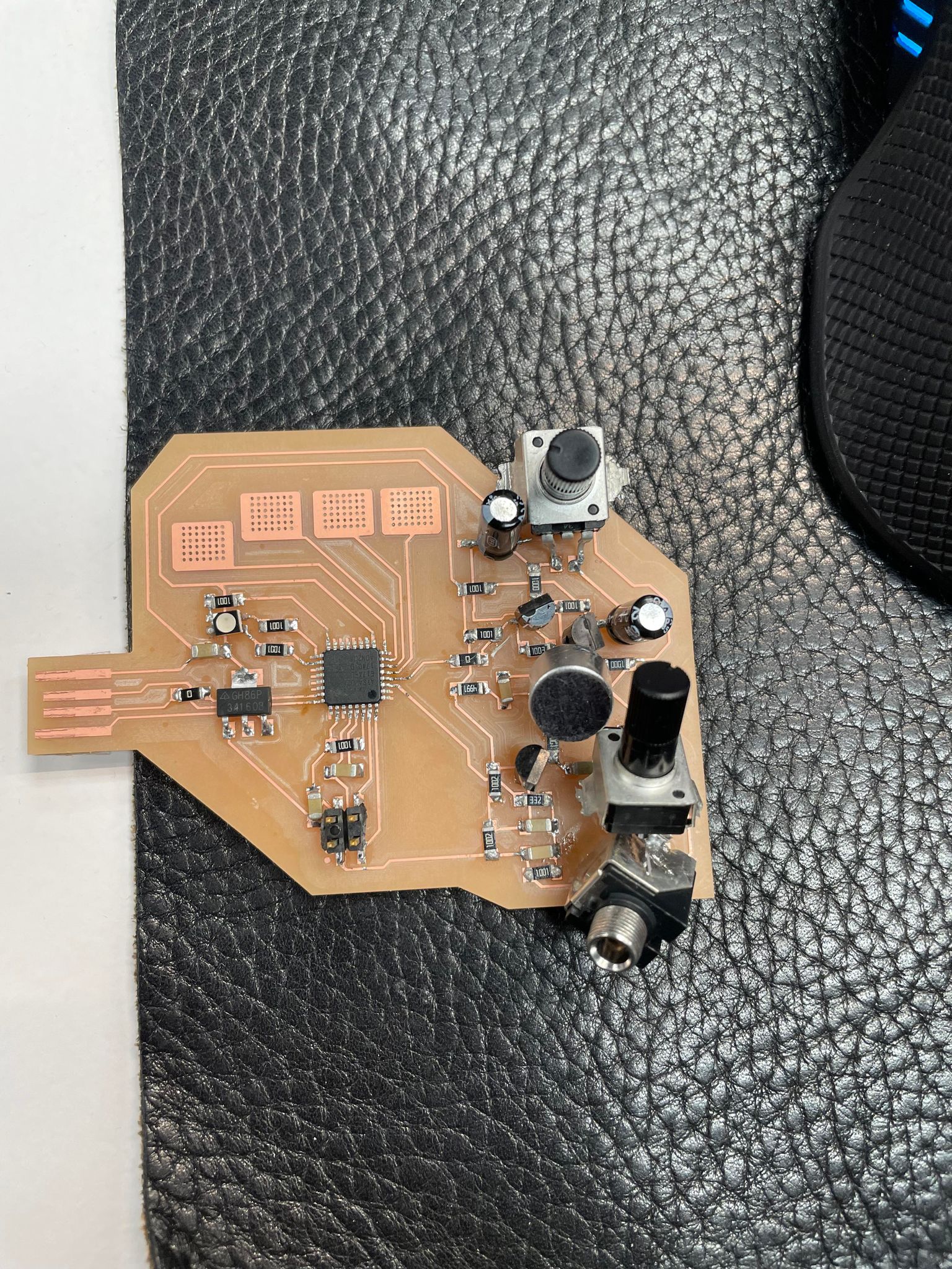 This led to some wonky looking circuit, but it all connected decently.
Now was time for flashing and testing!
After flashing with the SWD programmer and Arduino IDE with some help from my instructor Adai (we realised after a few tries that the first SWD was not working so he gave me another one which functioned!)
I then uploaded a simple code to make the LED flash in different colours when pressing the pads.
I had some issue with the preamp and amp... Before realising that the transistors used were not the same as in my initial testing, so I had to switch the pads around.
My cutting files for this week can be found here for the outline and Here for the traces and footprints.
This led to some wonky looking circuit, but it all connected decently.
Now was time for flashing and testing!
After flashing with the SWD programmer and Arduino IDE with some help from my instructor Adai (we realised after a few tries that the first SWD was not working so he gave me another one which functioned!)
I then uploaded a simple code to make the LED flash in different colours when pressing the pads.
I had some issue with the preamp and amp... Before realising that the transistors used were not the same as in my initial testing, so I had to switch the pads around.
My cutting files for this week can be found here for the outline and Here for the traces and footprints.