8. Electronics Production
This week I worked on producing a PCB. During group work, we learned how to use the Roland milling machine to mill the board. To produce the milling path files, we used Mods. During group work, we learned to use the Mods, to produce the necessary .rml files for milling.
Mods
The workflow on Mods is:
Open the Mods website Right click on white page -> open program -> open server program -> Roland-SRM20 -> PCB png. I did not want to use websocket device, but I wanted to save the output to file. For this reason I deleted the Websocket device by selecting delete button. Figure Then I added a save file module: right click on the page -> modules -> open server module -> file -> save Then I connected the Roland SRM-20 Miling machine box to the save file box by clicking the Roland SRM-20 milling machine - outputs file and subsequently the save file - inputs file boxes. This connected the outputs file to the inputs file with a line.
I downloaded the test traces (linetest.traces.png file) from the Fab Academy pages under CAM -> traces.
Then, from the read png box I clicked select png file, and chose the downloaded png file. After this, in mill raster 2D box I modified the tool diameter to be 0.2 mm, and the cut depth to 0.05 mm. From the Roland SRM-20 milling machine, I set the origin to zero -> x:0, y:0, z:0. Then, from milll raster 2D I clicked calculate, which produced me the milling path file (.rml file), that I could use in the Roland milling machine.
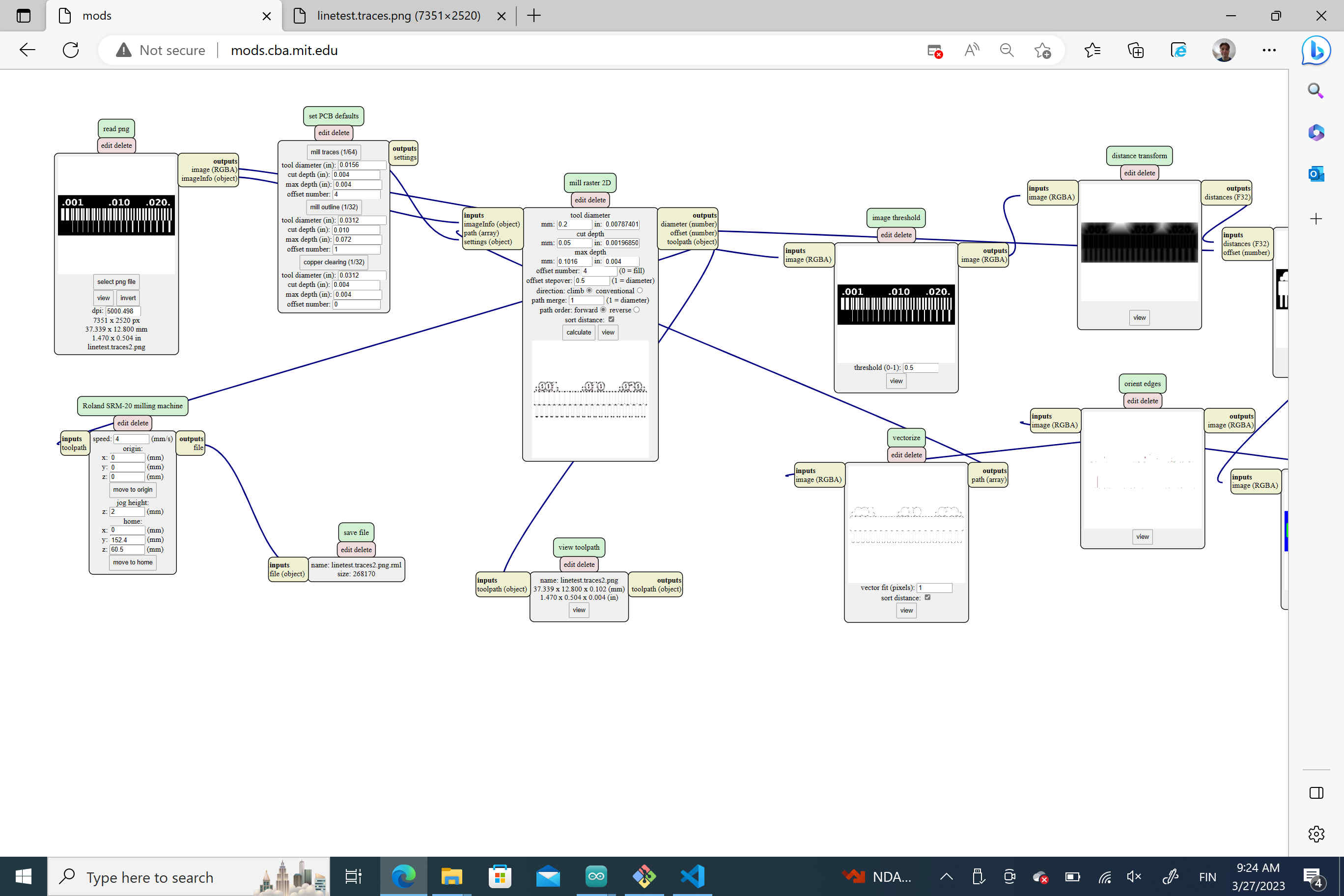
We also created paths to cut the test traces out from the board. For this, we would use 1 mm milling bit, and would cut deeper, so we set the tool diameter to 1 mm, cut depth to 0.6 mm and max depth to 1.8 mm.
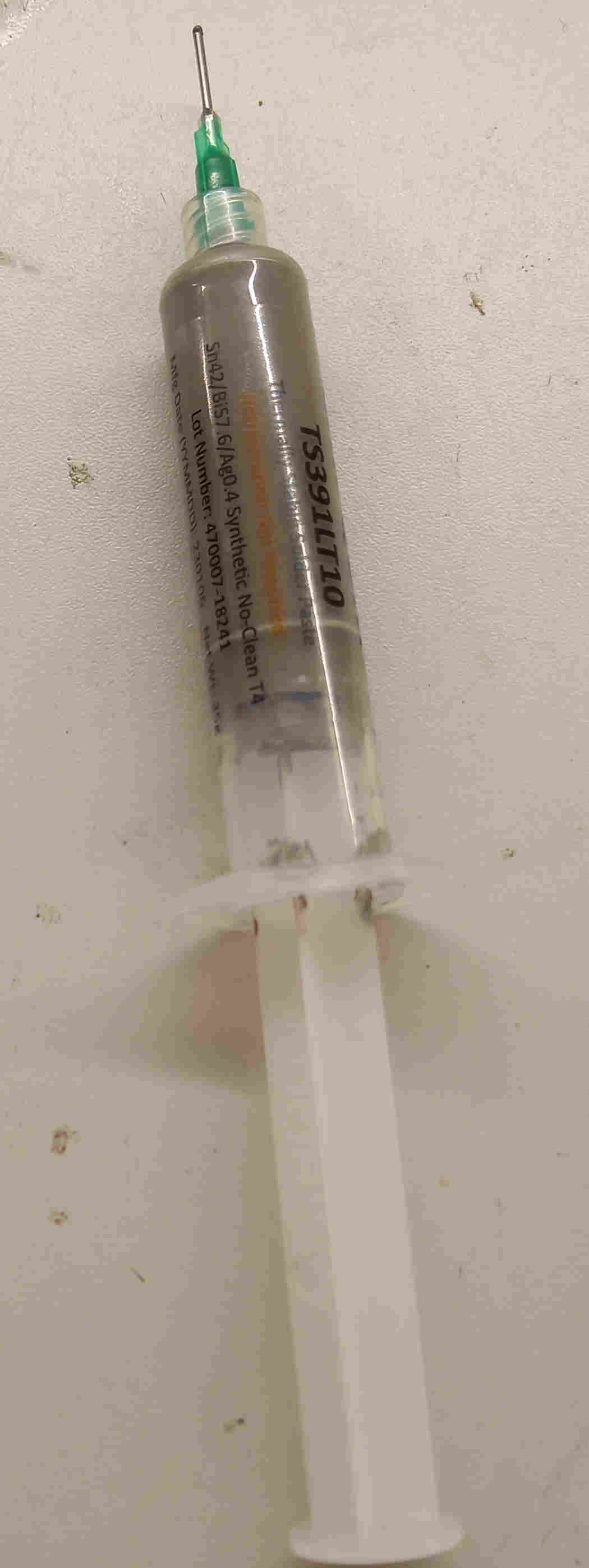
We also learned how to use LPKF milling machine, and solder paste and the reflow oven, which we used for soldering few components (button, led and resistor). We also learned hand soldering, which we used for soldering the other components. I had done some simple hand soldering earlier, but in the milled PCB the connections were a bit smaller than what I had done earlier, which caused some problems. Luckily, there was tin-sucking tape (solder wick) available, that I could use to correct the soldering.
Roland milling machine
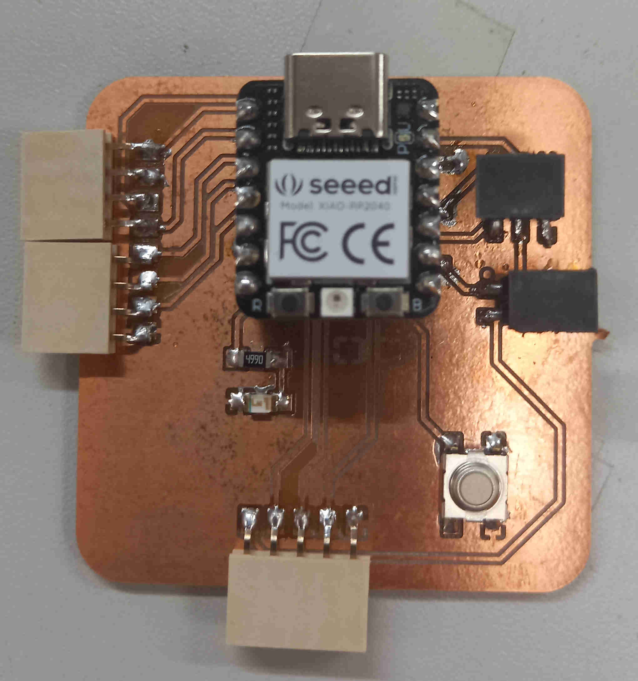
I tried to mill the circuit board that I had designed during electronics design week (my own design shown last). I got lot of useful help from Hannu Liedes and Ivan Milera as well as Aleksi Myllymaki who were around in the lab when I was working there. Hannu’s web pages on electronics production were also helpful when trying to remember the settings.
I output svg files from KiCad, and I used Mods to create the milling path files for the Roland cutter. There were few things I needed to do: I had to modify the svg files using inkscape. I used Mods to make the milling paths.
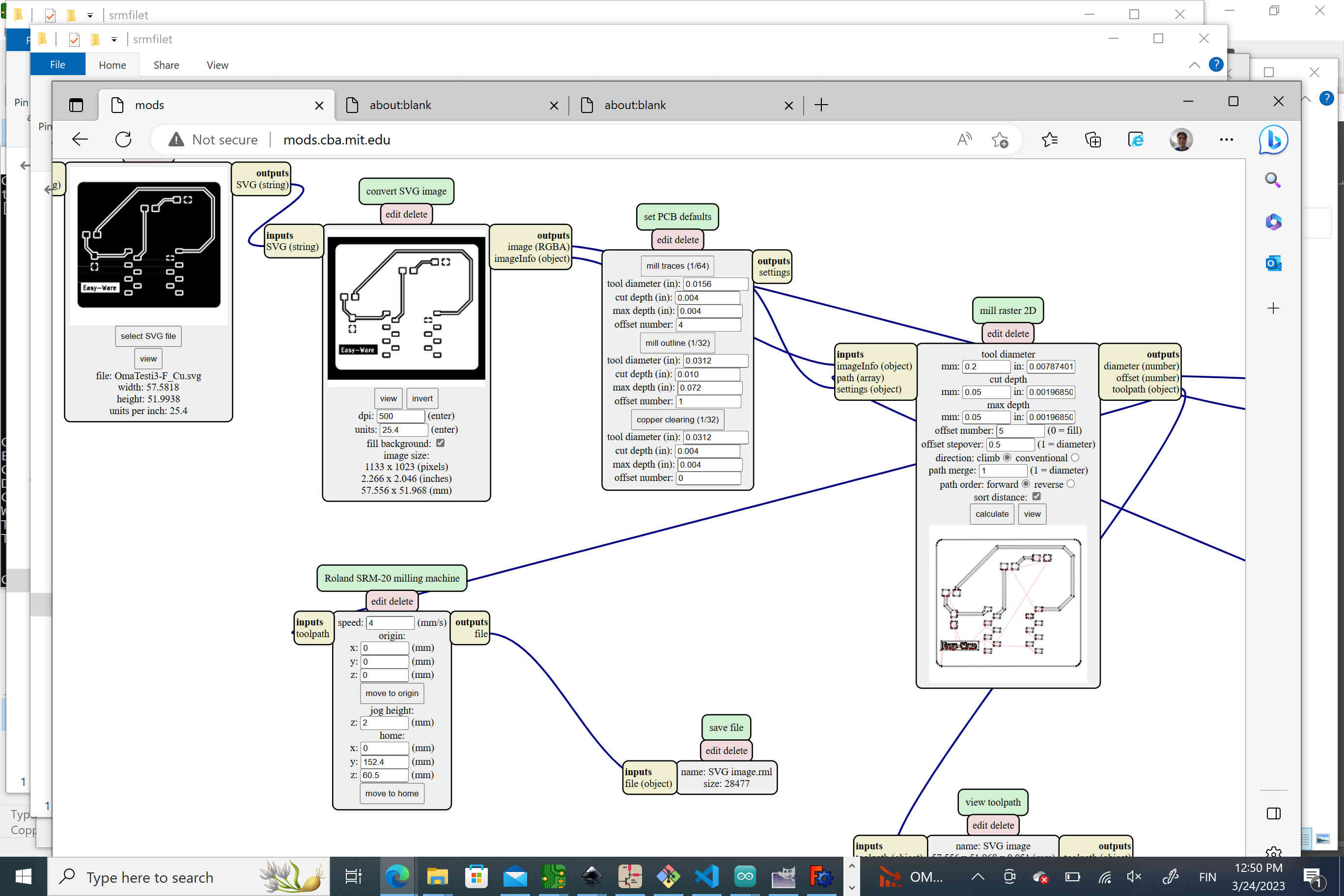
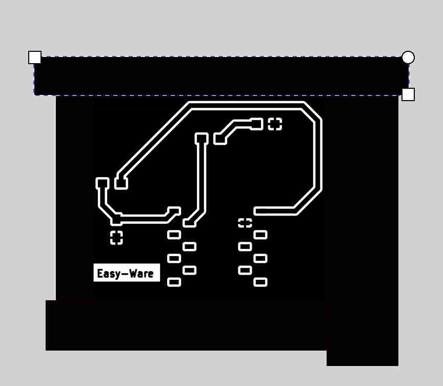
It became apparent that to make only the interior paths I needed to remove the edges before using Mods. I added black edges over the white edges, so that whole layer was covered by black, except the lines that would be milled.
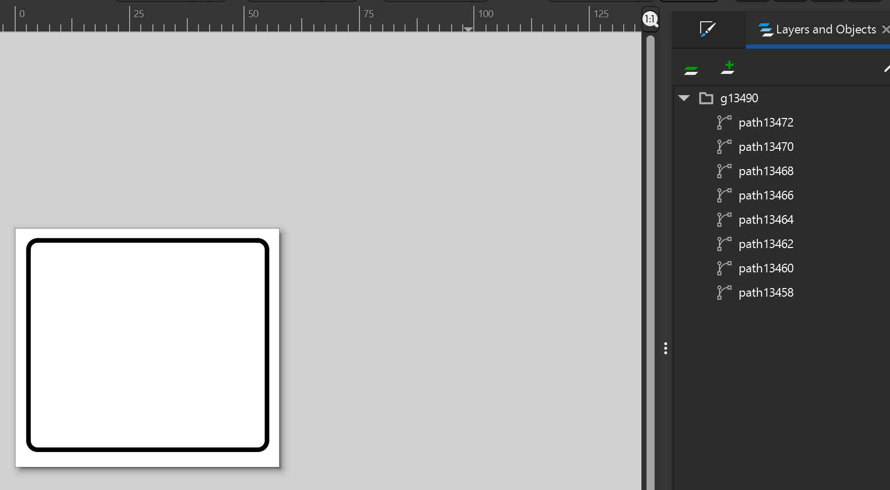
Also there was problem when using the Mods for cutting the boundaries. It appeared that KiCad output contained several layers. I had to modify the boundary lines in inkscape too. I did this by selecting Objects -> Layers and Objects. There I deleted the extra lines, and left only the paths that consisted of one surrounding line. Then I saved and used that svg file in Mods.
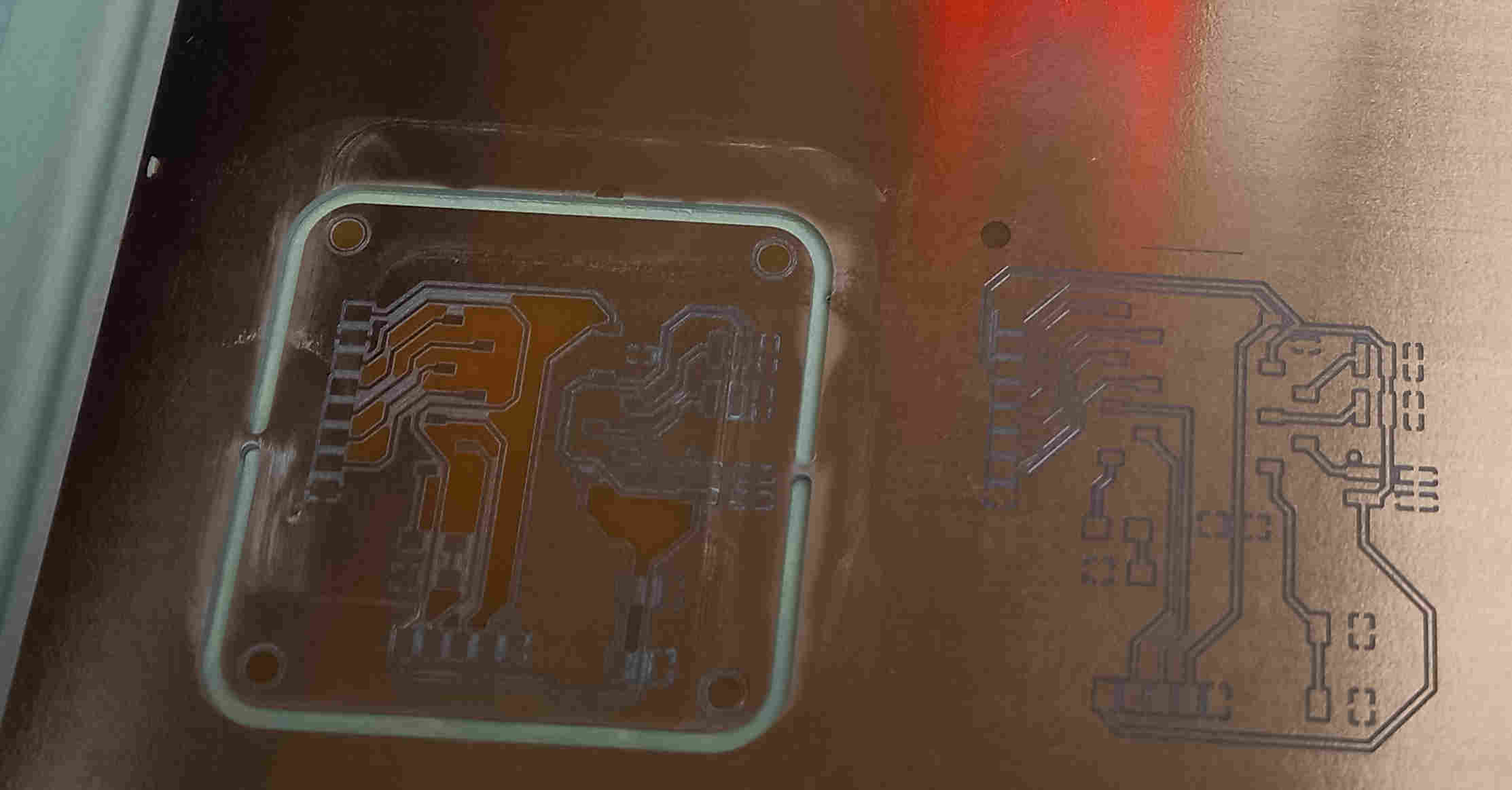
The problem was that the board was not flat on the surface, and the milling bit did not touch the board at all positions. I tried to reset the zero in z-direction to that place where the bit did not touch the board, and I milled again. However, the board had probably slightly moved and the lines became too thin (and nonexistent). Some places seemed quite ok however.
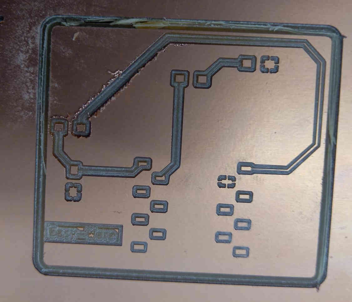
I tried to increase the width of the lines, so that in case I needed to mill again, they would not be totally removed. As a sidenote, the whole line could be selected by pressing u after selecting one segment. I set the line width to same as the pad width, 1 mm. I also tried to straighten the board.
However, I encountered also other kinds of problems. Sometimes the double sided tape did not hold well, and the board moved during milling. I noticed that in the underlaying wood plate, there was an higher edge, which was probably left to maintain the board in place. I layed the board against it on one side. This helped to keep the board still a bit better. I also noticed that the ground pads became separated from the ground. I probably should not use corner separation for the ground pads, and I could also make the ground pads bigger, say 2 mm.
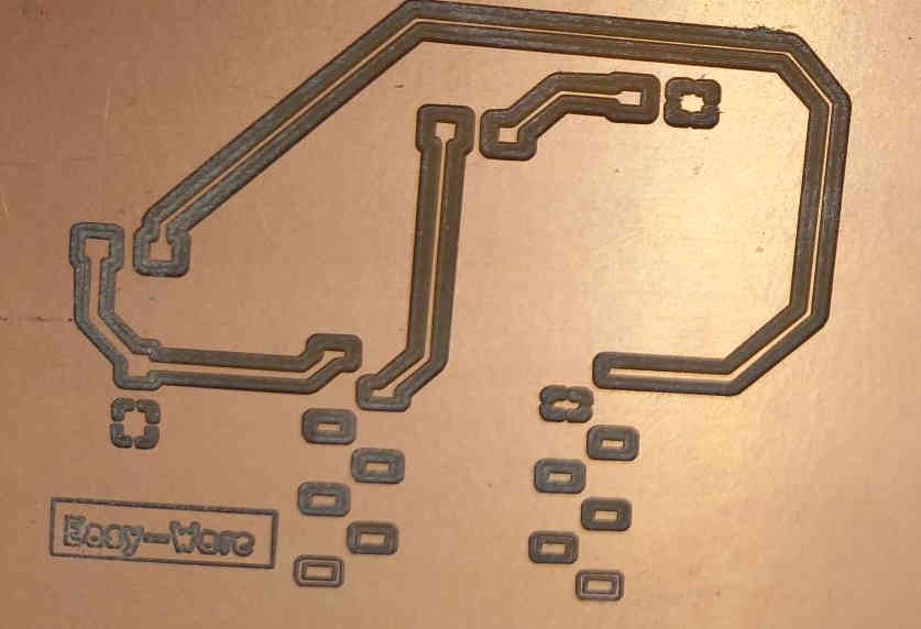
Trying many times, I can see that it seems not to be easy to mill with Roland machine, and this experience made me respect the students who succeeded in doing so. I may try again later time. Perhaps it was not a good decision to re-set the zero and mill again, but if the milling goes wrong, what else I could do… I think it would be good idea to 1. set pad sizes larger, say 2 mm, and the lines as 1 mm and in case I would mill again, they would still be ok. I should not use corners in ground pads, but instead use vertical or horizontal lines. Also I could experiment with milling depth, so that it would cut better in single milling.
LPKF milling machine
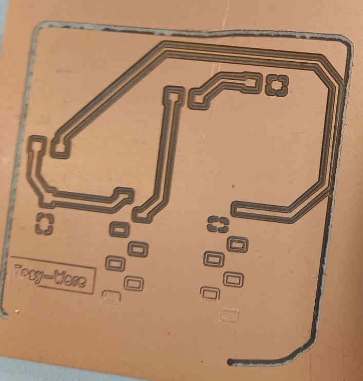
I had designed a board during electronics design week. This week was dedicated to milling it.
We used The LPKF milling machine, which was operated with Circuitpro program.
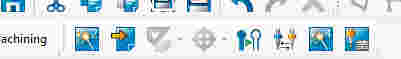
The workflow consists of going through the stages shown by the icons in the upper left hand corner.
Select type of process -> process PCBs -> next
How many layers is the board going to have? -> Single sided top -> next
What kind of substrate are you going to use -> FR4/FR5 -> next
Summary -> Done
Import -> Select Gerber files -> Open
The Gerber files: paths and edge cuts.
From import dialogue, check both files. Visually inspeced that they look correct -> OK
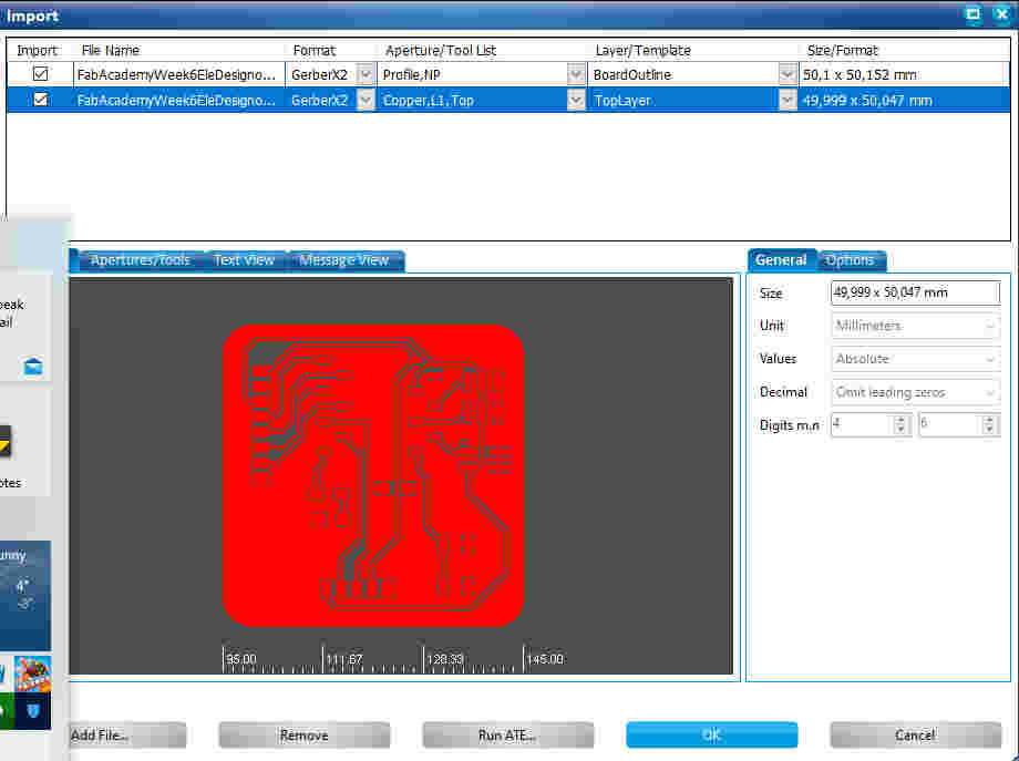
CAM view shows the board.
Technology dialog: Isolate tab -> Universal Cutter 0.2 mm was chosen. I choosed also End Mill 1 mm. Contour routing -> Copper layer thickness 35 micrometers. I chose Vertical gaps for the Contour Routing Method
The screenshot shows the results, they seemed ok -> Close.
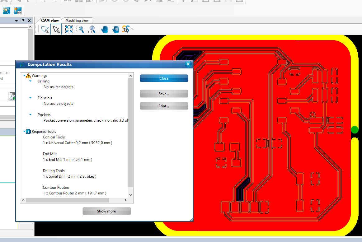
Open the dialog to edit the contents of the tool magazine.
Universal Cutter 0.2 mm Tool Life is showed 100 % spent, but since FR4 settings have been used although real material mostly is FR1, the tool is still ok. -> OK
Selected Start the Board Production Wizard from the icons in upper left corner.
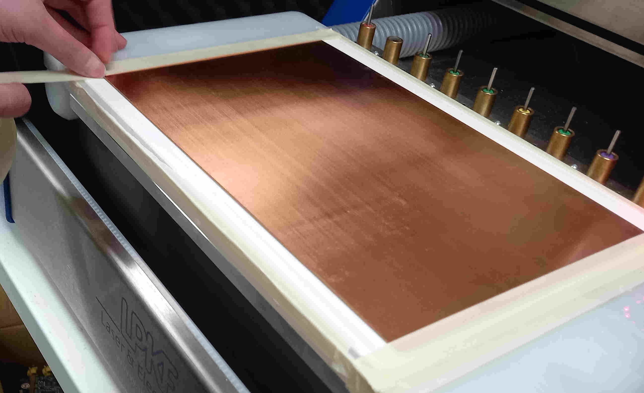
Program asked to mount the material
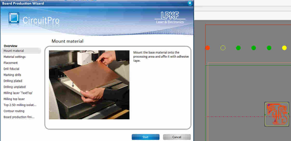
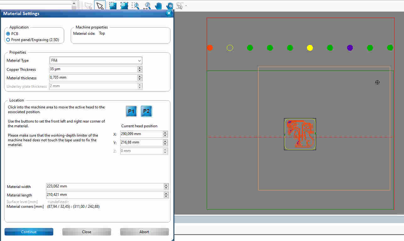
Material Settings Dialogue, Location -> Click into the machine to move the active head to the associated position P1, P2. -> Selected suitable locations for the positions by clicking (The tool head moved to the positions). -> Continue
Placement -> moved the board to the correct place.
Measure milling width -> Horizontal milling line -> Line length 10 mm -> After checking the width, I cilcked Accept width
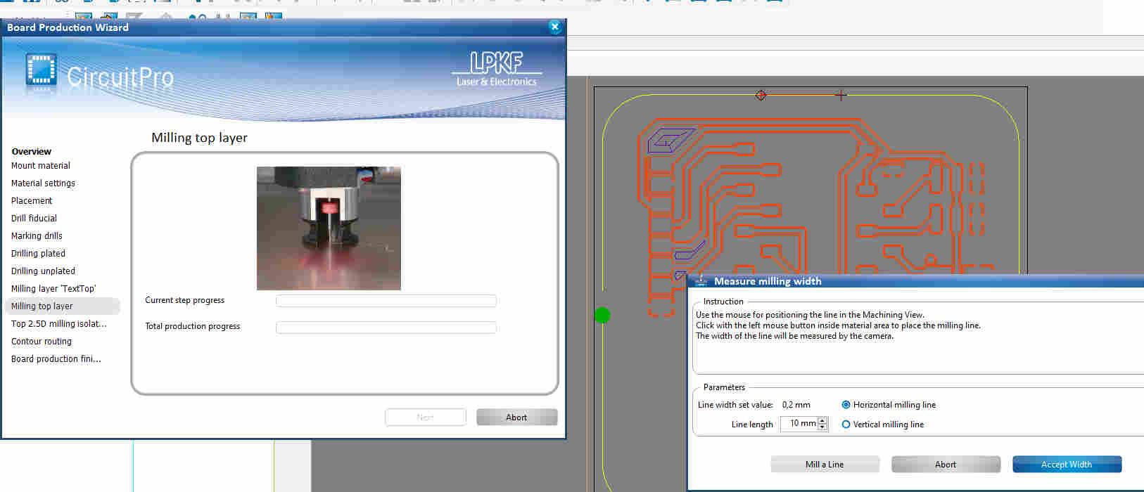
Warning message, that the position collides with the bounding box. It had been selected so that the line does not cause problems -> Ignore
Confirmation of focus height -> yes
Measure mode point to point, selected the points from the camera window. Seems about correct -> Accept width
Milling the connections
The End Mill line width measurement: Measure milling width -> line length 10 mm -> Accept Width.
Milling the PCB boundaries.
Preparing to disconnect machine -> Move head to a safe position to switch off -> Yes.
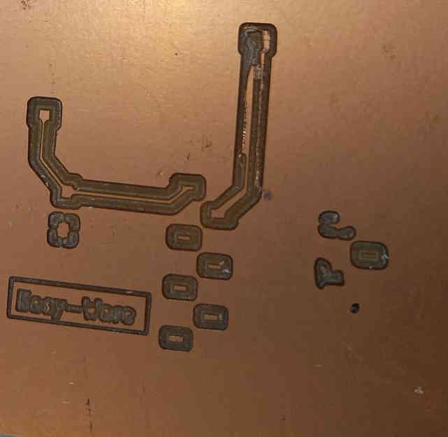
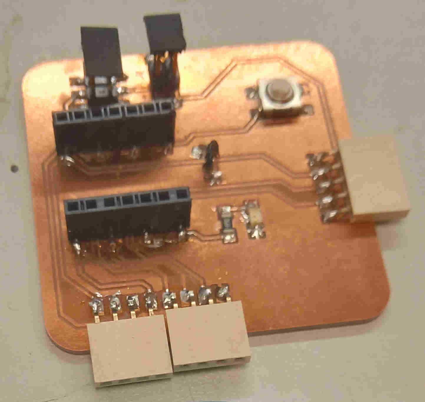
After milling the board, it was time to put the components on it. We learned both using solder paste and reflow oven, and hand soldering. With solder paste we soldered button, led and a resistor. The other components were soldered by hand.
First I laid all the components on their approximate positions.
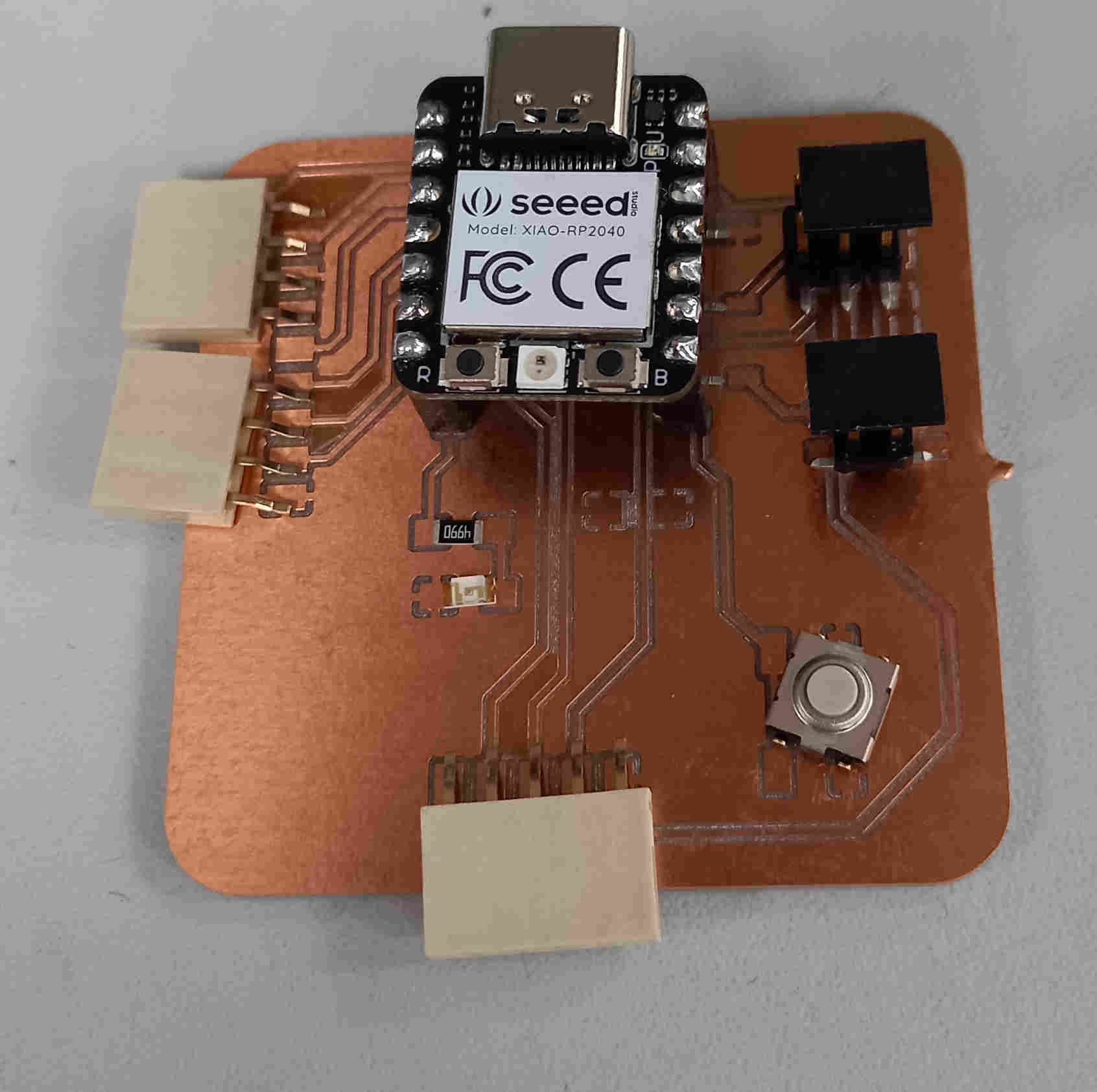
Then I put the solder paste on the board for button, led and resistor, and laid the components on them.
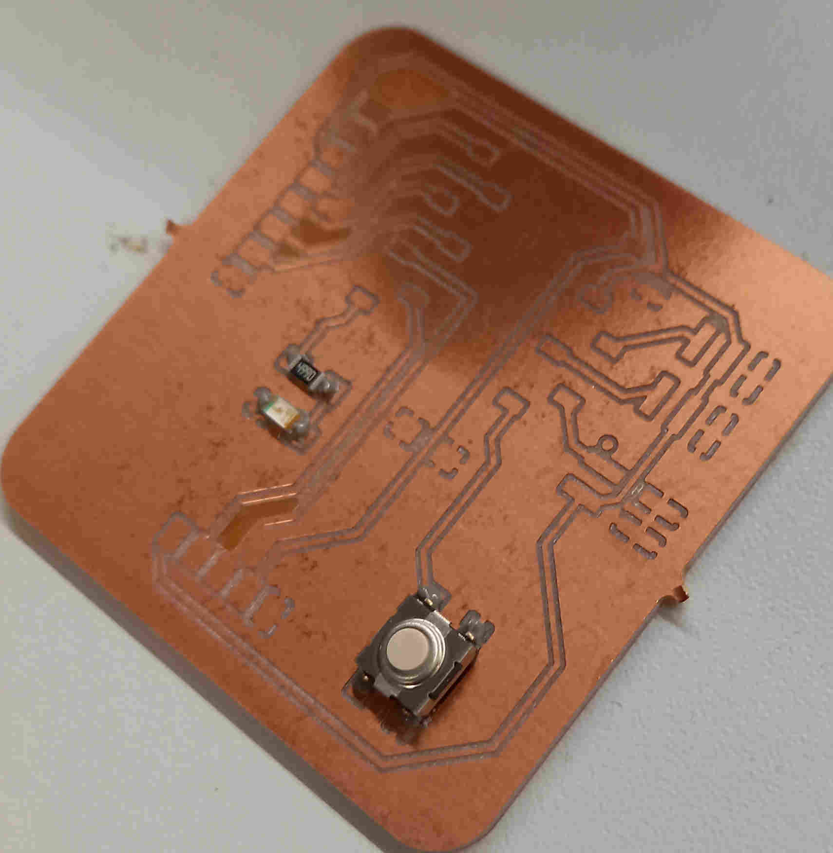
Then we put the board to reflow oven, and the components were soldered.
After this we proceeded to hand soldering the rest of the components. The traces were a bit thinner than what I was used to, and I had some problems with making short circuits. I needed to use solder wick to get rid of the short-circuits.
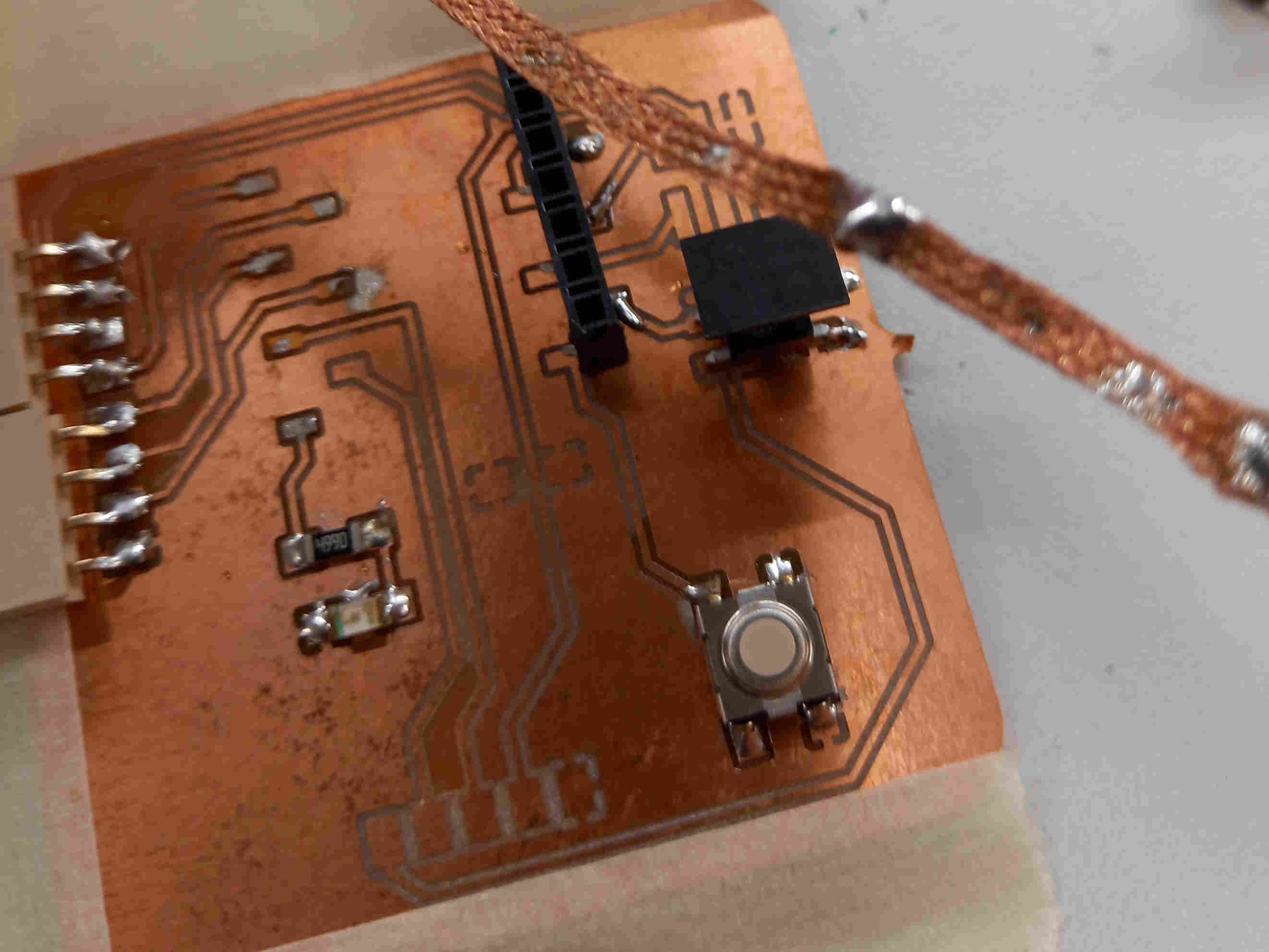
I had made the design to include a zero ohm resistor to connect two separate grounds. I soldered a jumper wire to the designed place.
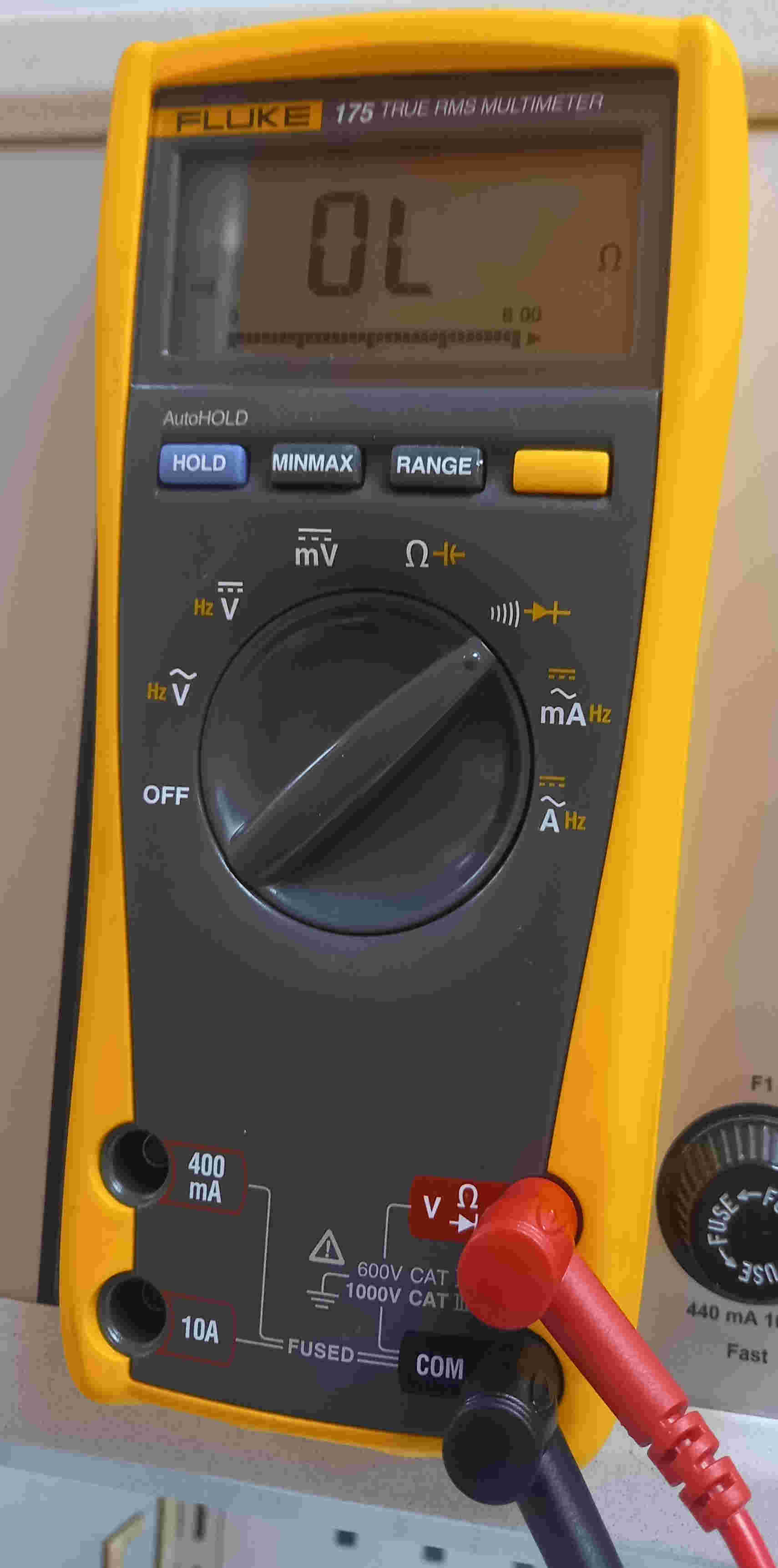
I used multimeter to check that grounds were not connected to any pins, and that the grounds were connected to each other.
Circuit board led
I had learned to program the microcontroller during embedded programming week. I tested the operation of the circuit board, which I could control with pushing the button. I modified the button example code provided by the Arduino IDE (file -> examples -> digital -> button), so I could control the led, which is connected to pin D6. The button is connected to pin D7.
I had some trouble with the button, and started complaining about it when the other students where in the class. They told me that I should modify the example button code to include pull up resistor. To do this, I found that I should include INPUT_PULLUP to the pinMode command: pinMode(buttonPin, INPUT_PULLUP); After adding this argument, the button started working and I could test the led. The modified code is here.
During output devices week I tested the digital pins D0, D1, D2, D8, D9, D10 to check they were properly connected.