6. Electronics Design
This week we took a deep dive in electronics design. At least it felt so, since this was new to me; I had previously tinkered with breadboards and jumper wires, but I had never designed a PCB board. We used Kicad software for designing a circuit board with guidance from our instructor Antti.
During group work, we measured the power consumption of a LED by measuring the current drawn by the USB. The color output of the LED affected the power consumption. Also we measured the power consumption of the smaller builtin LED.
Printed circuit board design using Kicad
First, we downloaded the fab library from the fabacademy gilab site fab academy gitlab site.
After setting up the fab library in Kicad, we started to design the schematic.
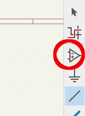
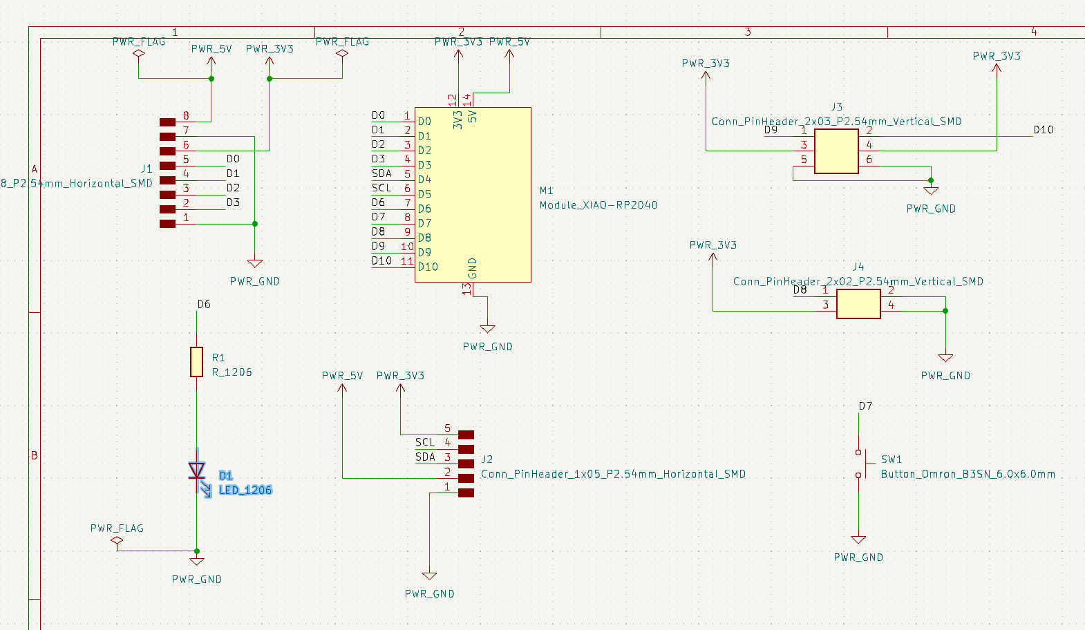
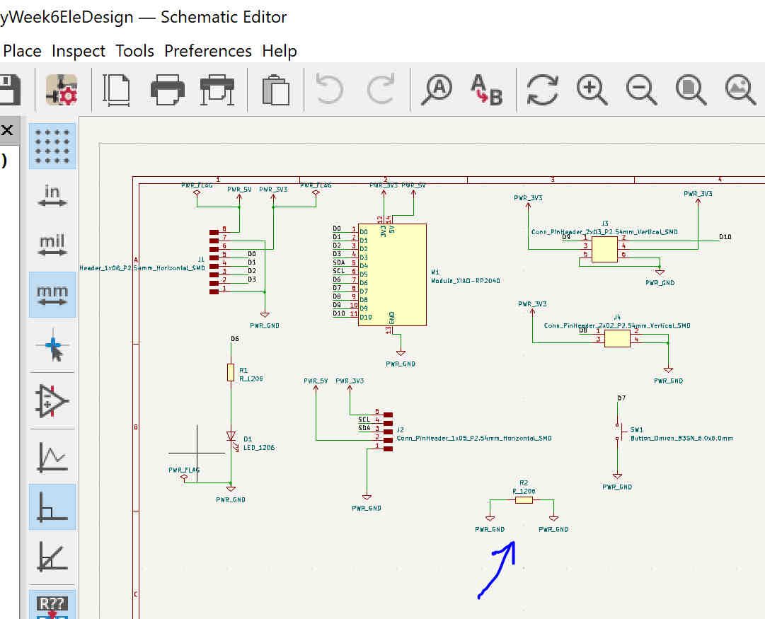
We added all the necessary components for the test circuit board. The components could be added by pressing letter "a" or by choosing add a symbol from the right hand menu, as shown in the figure below.
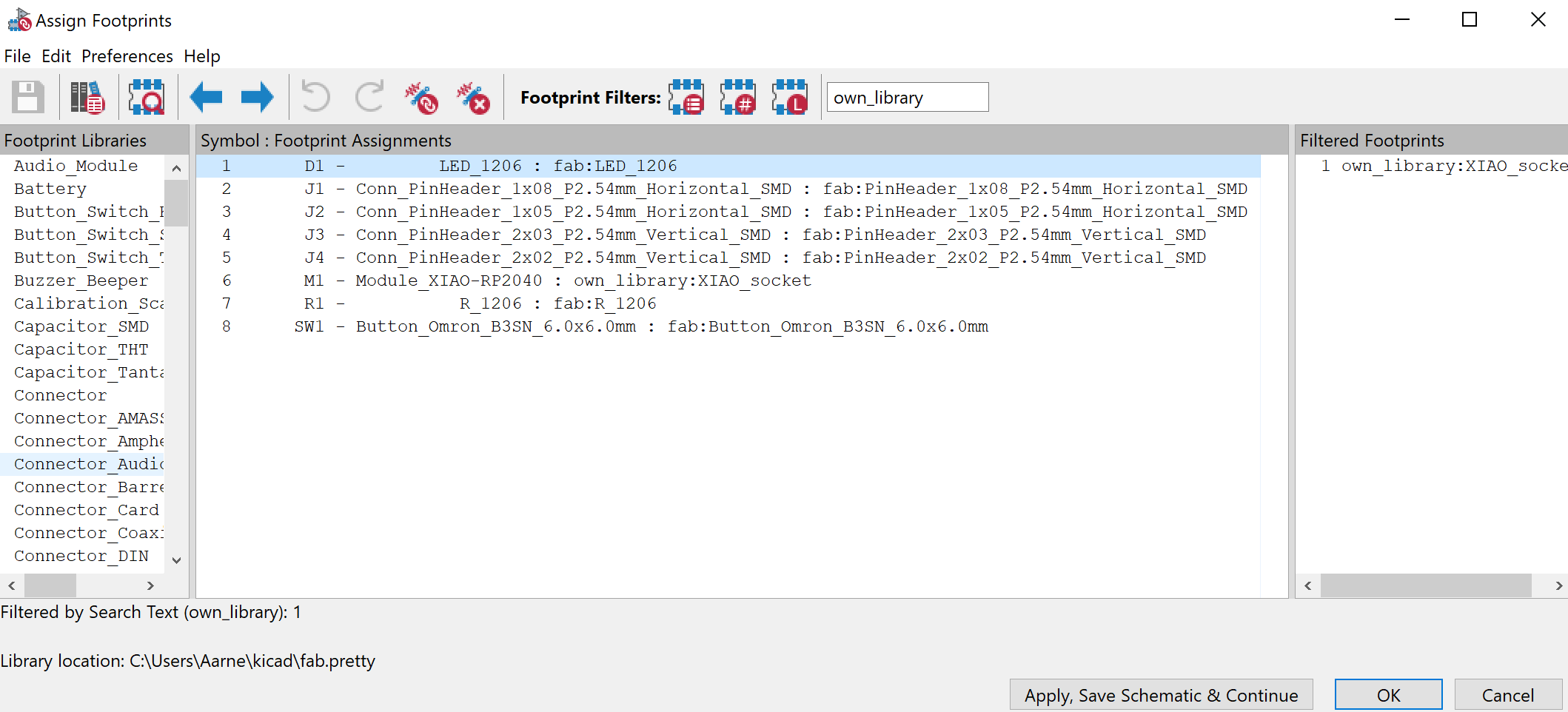
We set up the footprints of the components, so that they would take the right amount of space in the board. This was made by choosing tools from the upper menu and from there: assign footprints.
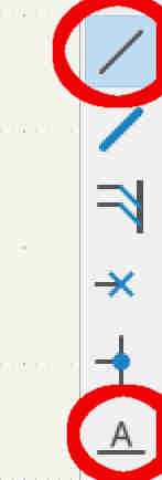
Then we added wires and labels. The wires could be added by pressing "w" and labels by pressing "l", or by using the menu selecion as shown below.
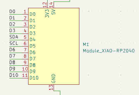
We connected the components with the wires. Then we added flags for ground and power pins, so that the program knows which are the current source and ground.
After this we chose "tools" from the upper menu and there: "update PCB from schematic"
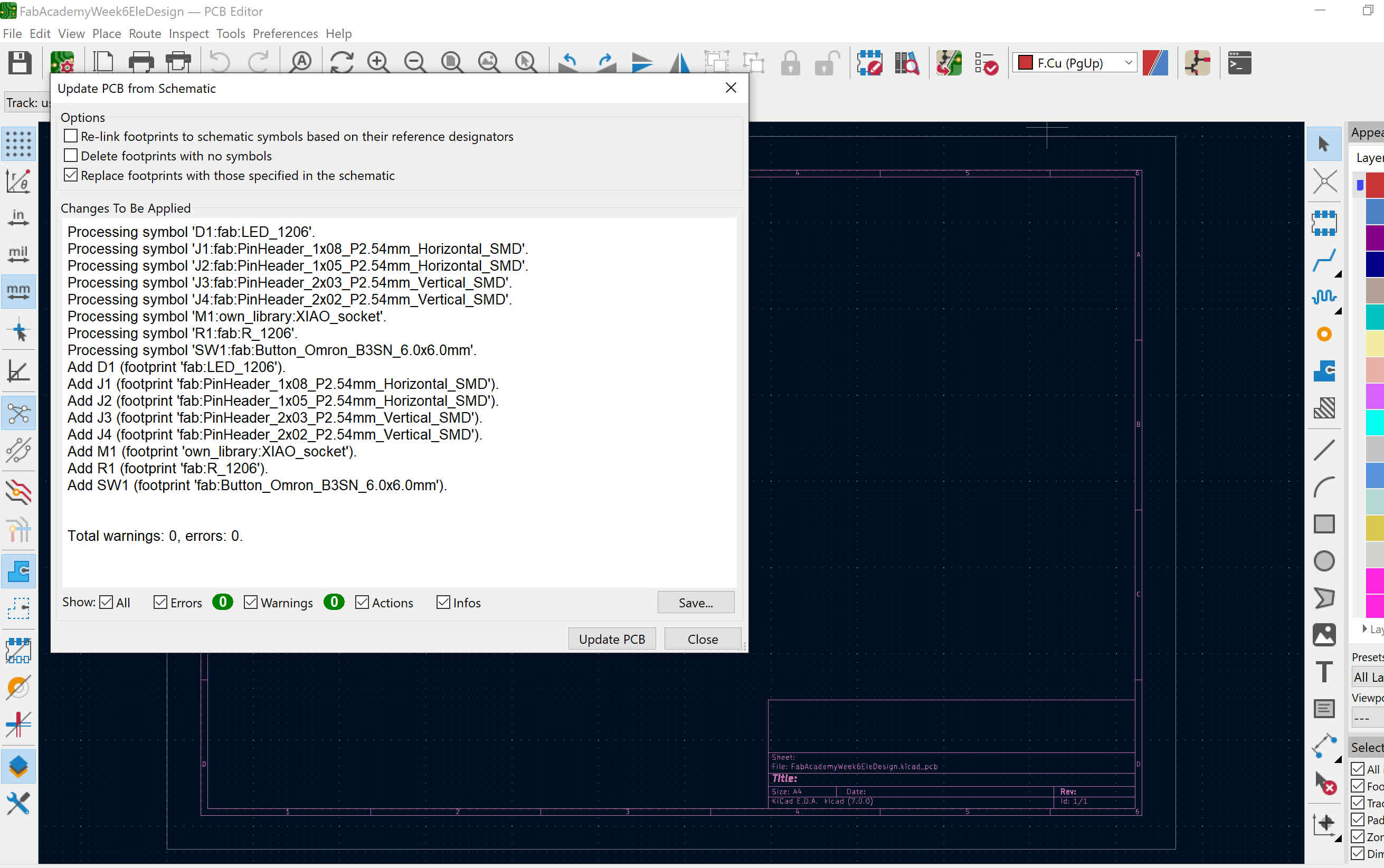
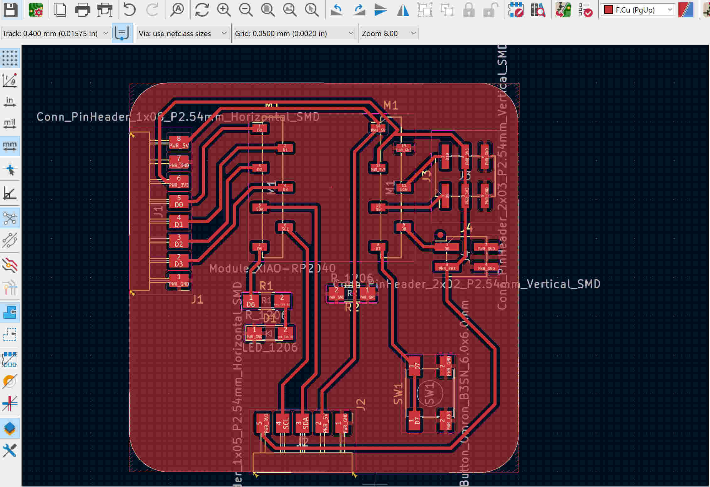
This yielded a window with the components laid out next to each other.
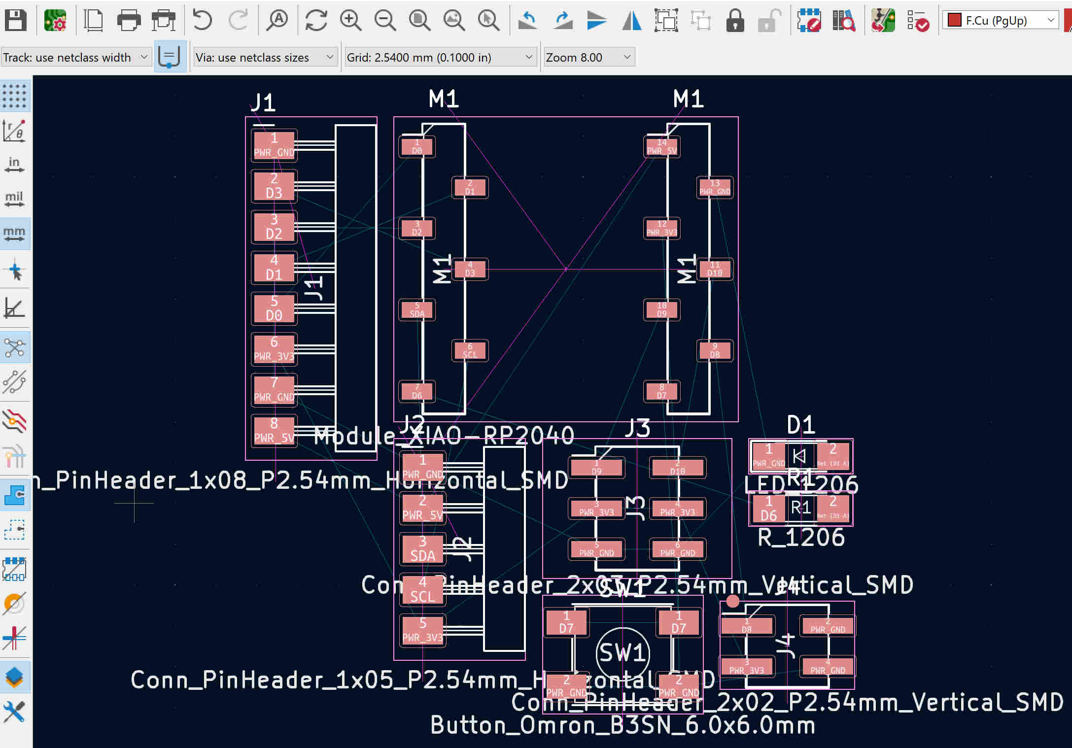
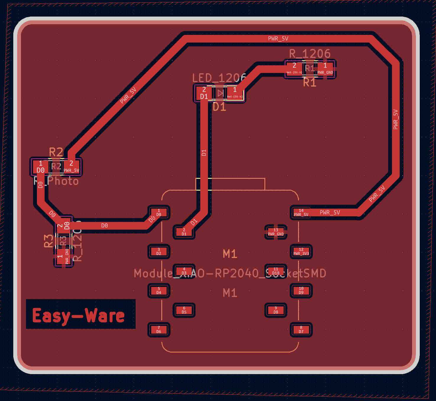
I moved the components in a better order, drew edges to the board, and routed the connections between the components. I left the grounds unconnected at this point, since they would be connected to the large filled part of the PCB.
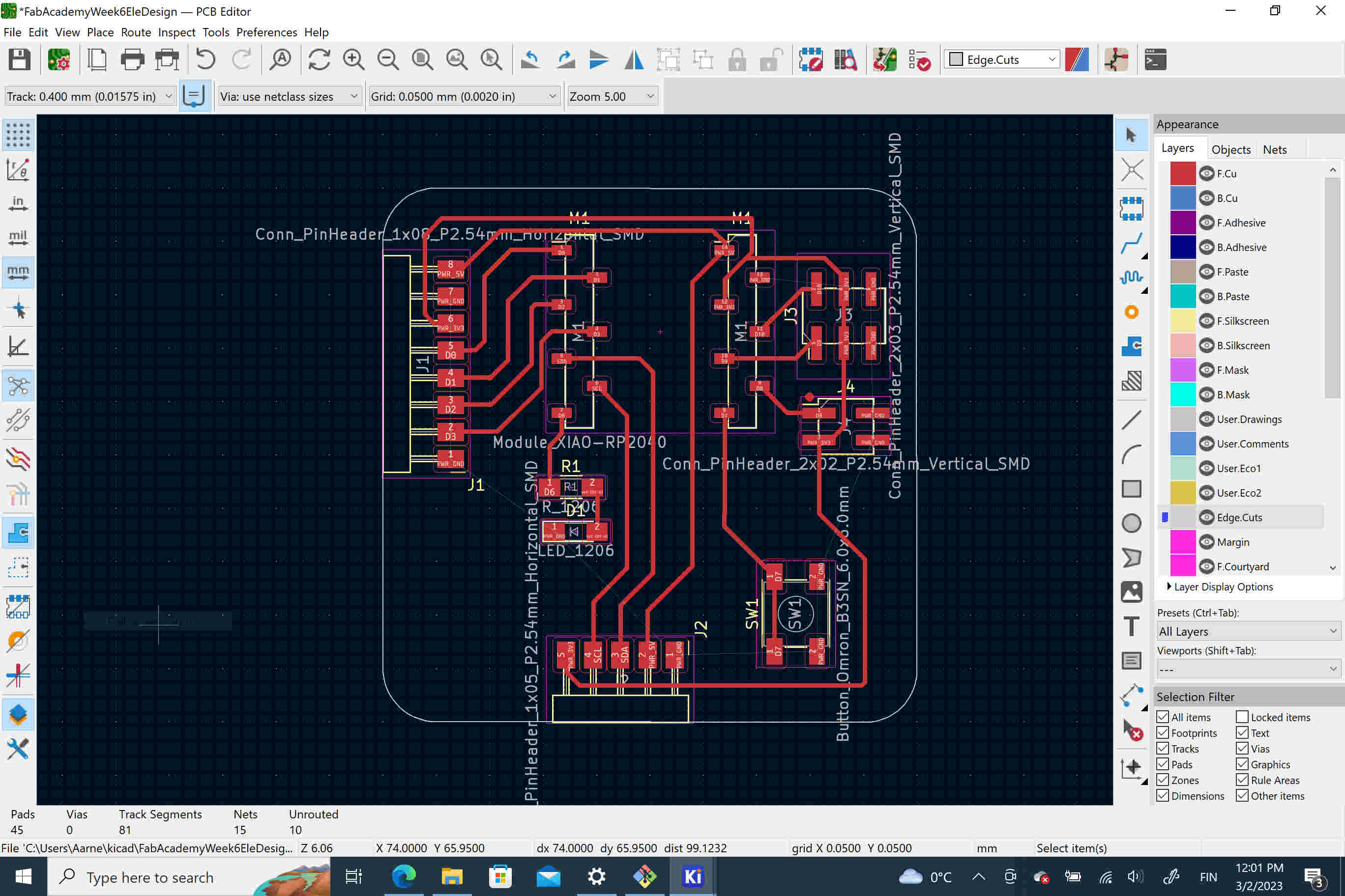
Finally, I selected "add a filled zone" from the right hand menu, clicked inside of the board region and selected F.Cu from left, and PWR_GND from the list. This filled the board region with the copper, except the connecting lines and pins that were not connected to ground. I had trouble with making the connections so that there would be only one unified ground area. I decided to solve this by adding a zero ohm resistor between two ground areas.
The ready Kicad circuitboard design file is here. The Kicad schematic file is here.
After working through the example, I decided to try to design my own board. I tried to design a PCB board for the photoresistor controlled led project, which I did using breadboard and jumper wires during Embedded Programming.
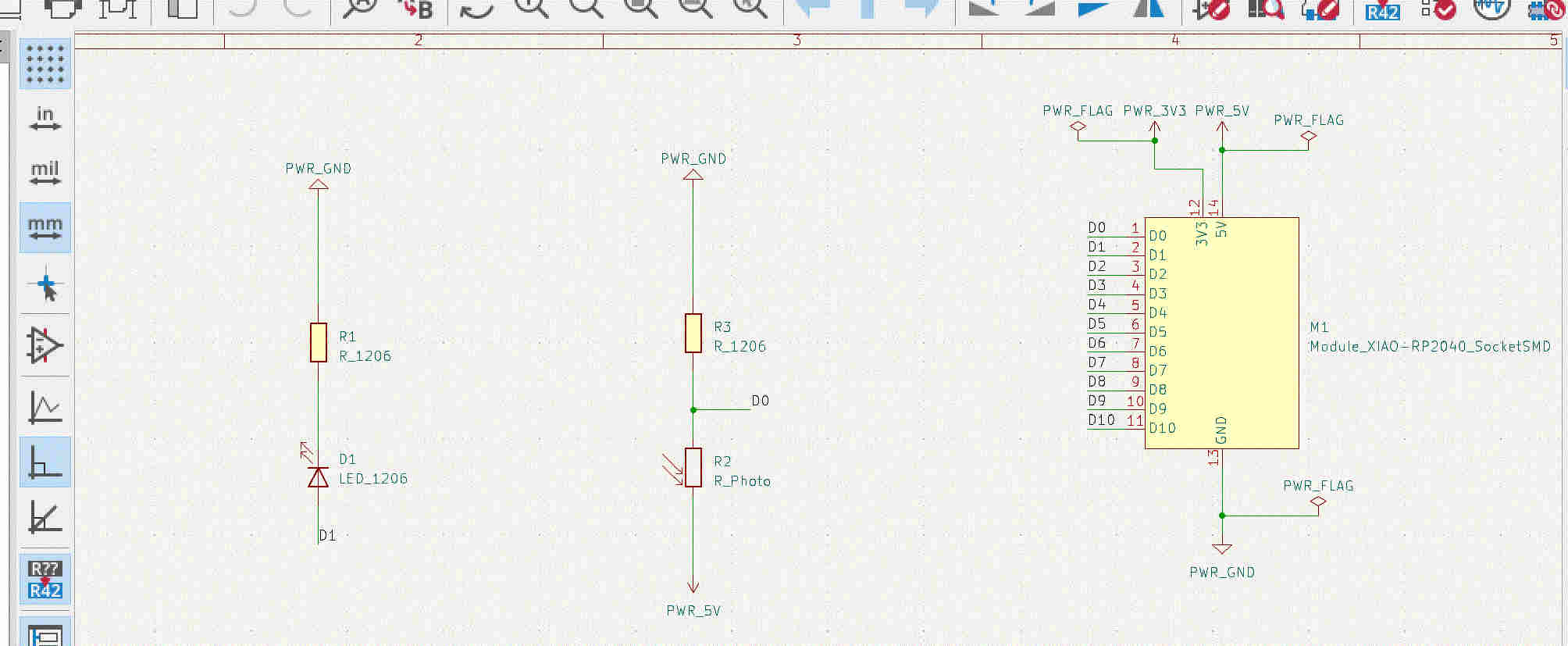
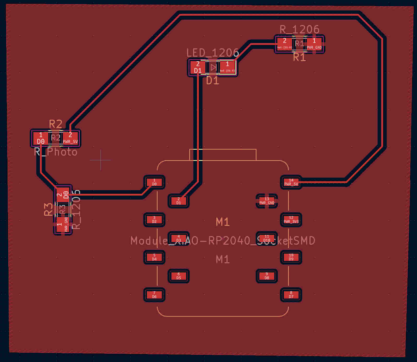
During regional review, Jani suggested me to increase the connection width, which I did. Later when I tried to mill the board, I inreased the widths even more so that I would not erode the lines, even if there was problems with the precision. I also added my own text tag to the circuit board design.
The final circuit board file is here.