Week 08 Electronics Production
Group Assignment
- characterize the design rules for your in-house PCB production process
- extra credit: send a PCB out to a board house
Result
- Please see our lab's site
Feeling and Thoughts
- We used smaller CNC machine than last week. And the end-mill is very thin like a hair. So one of the most important thing is to protect the mill. Especially 2 situations. One is setting up, we need to be careful when put the end mill on the machine if I dropped it, easily it would be broken. So I keep the cover on until the set up done. The second is configuration of milling, speed and cut depth should not be too much.
Individual Assignment
- make and test the development board that you designed to interact and communicate with an embedded microcontroller
- extra credit: make it with another process
Result
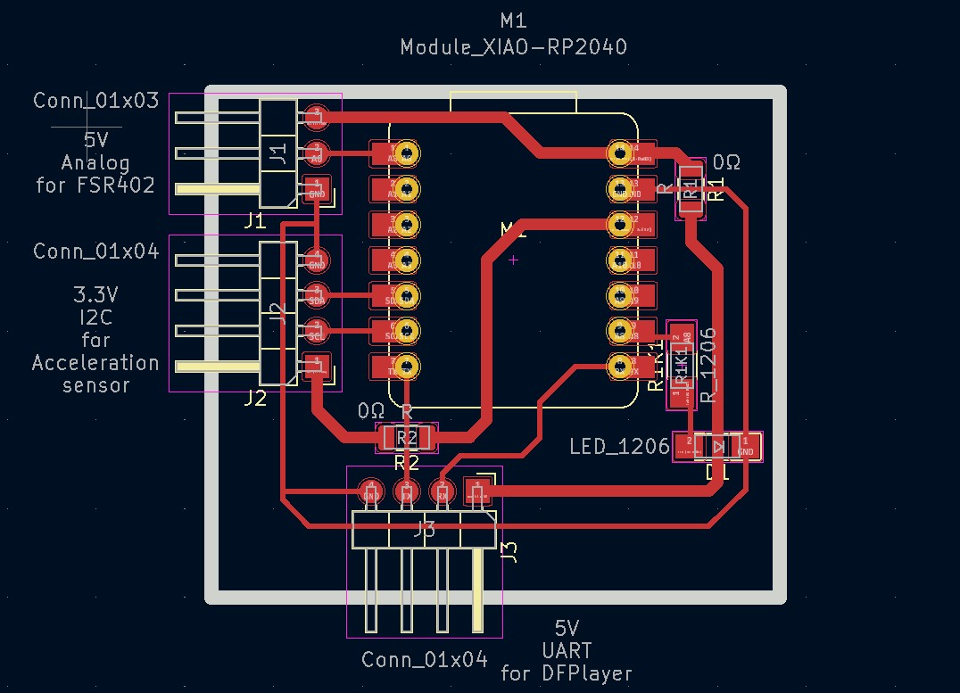
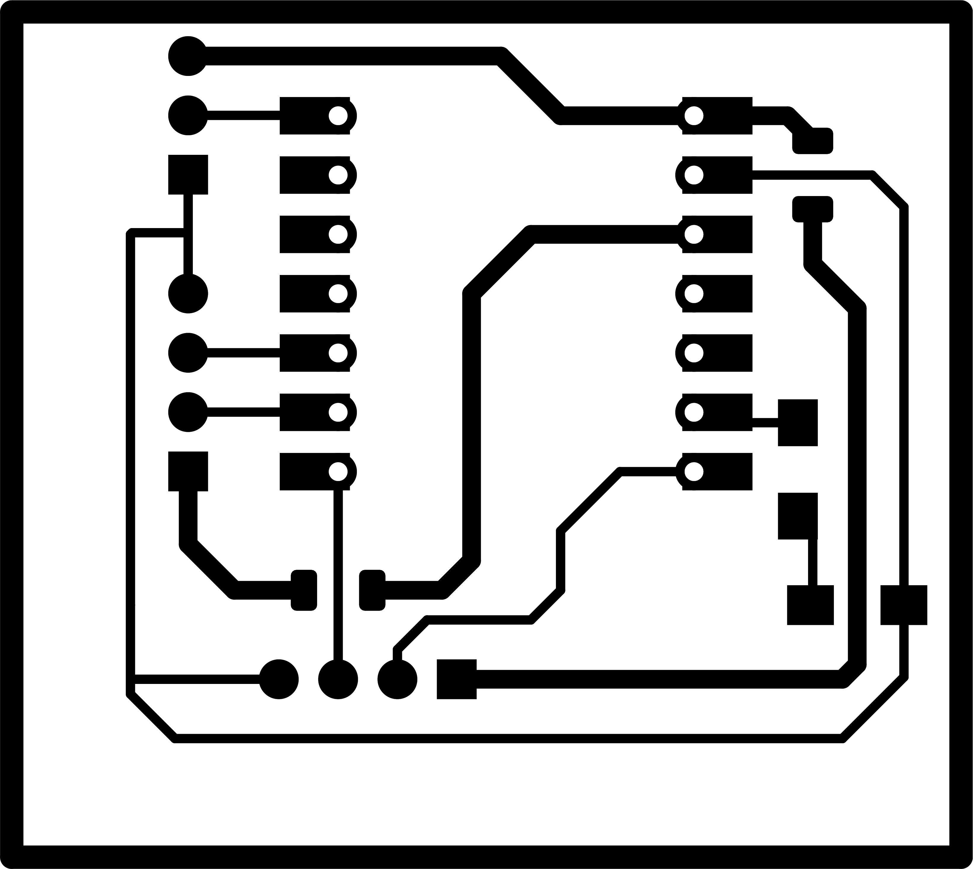
- I changed PCB design as below and milled for my final project.(original data: sch / pcb)
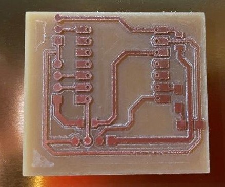
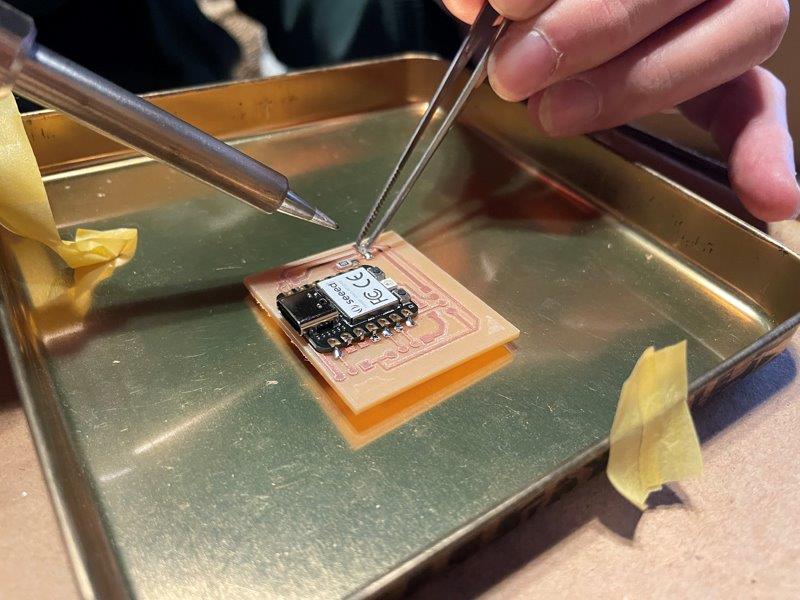
- Milled a PCB
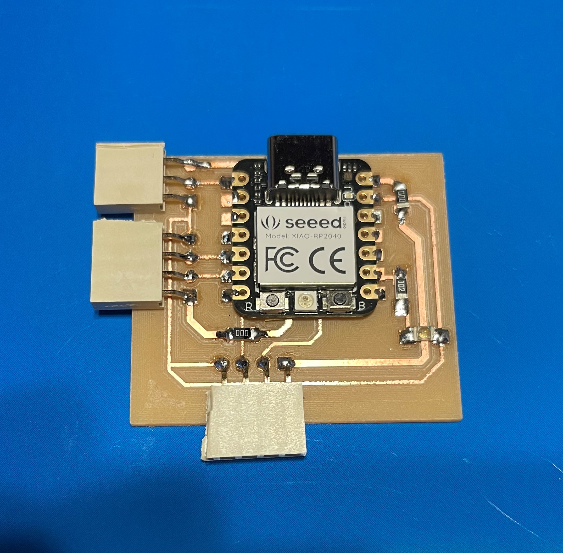
- And soldering.
Process to the result
1 PCB design with Ki-cad
- I did PCB design for the assignment of week6 as below.
- Based on advice from instructors I needed to change it below 2 points.
- I did not think about DRC (design rule checking) at all. For example the width of the line. Now I confirmed such rules in the group assignment this week.
- To make lines assignment simple, I put vertical connectors. But this is not durable.
- I just made PCB design for test something, but it would be better for my final project.
- For changing my PCB design, I checked VCC and communication io of my final project devices. At this moment I am going to use 3 devices as below;
- Force sensing: FSR402 / 5V / Analog
- Acceleration sensing: Sensor with MMA8452Q/ 3.3V / I2C
- Sound: DFPlayer mini / 5V / UART
- xiao2040 has all of io pins above, so I put xiao2040 as the controller of my board.
- I learned from instructor Adrian’s work that the pattern line can go under the controller, it made design simple.
- As a result I designed as below;
- Then extracted pattern and edge line (.svg) for milling
2 Tool path with Vcarve Pro (original file)
Pattern
- Imported the svg file above. And select only pattern for setting. Then start settings in the tool path window.
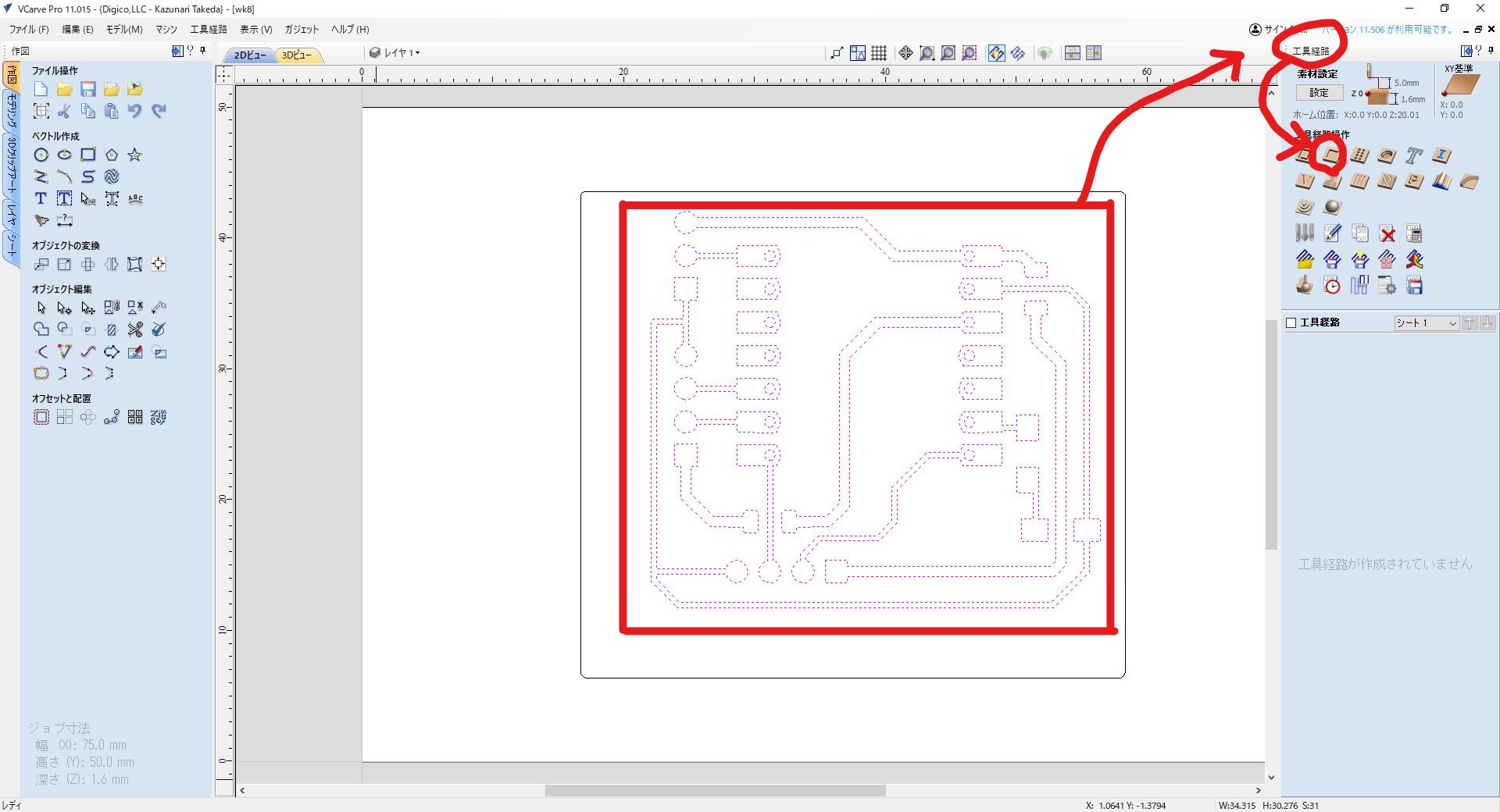
- Tool path setting is similar to week7 but this time "Pocket" setting is required for patterns. Select "Pocket" -> "Tool" window
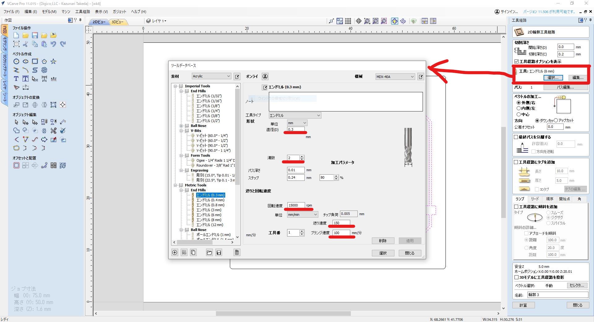
Settings as follows;- end mill size: 0.3mm
- cut speed 150 mm/min
- Number of path and cut depth setting.
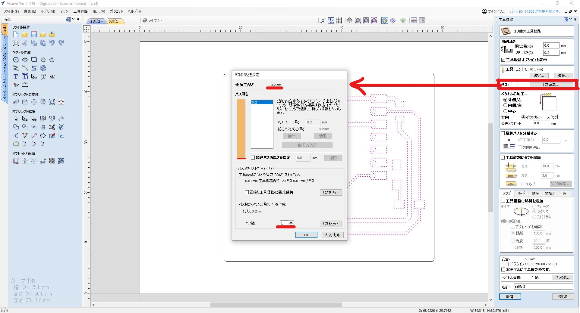
Settings as follows;- cut depth 0.2mm
- Number of cut 1
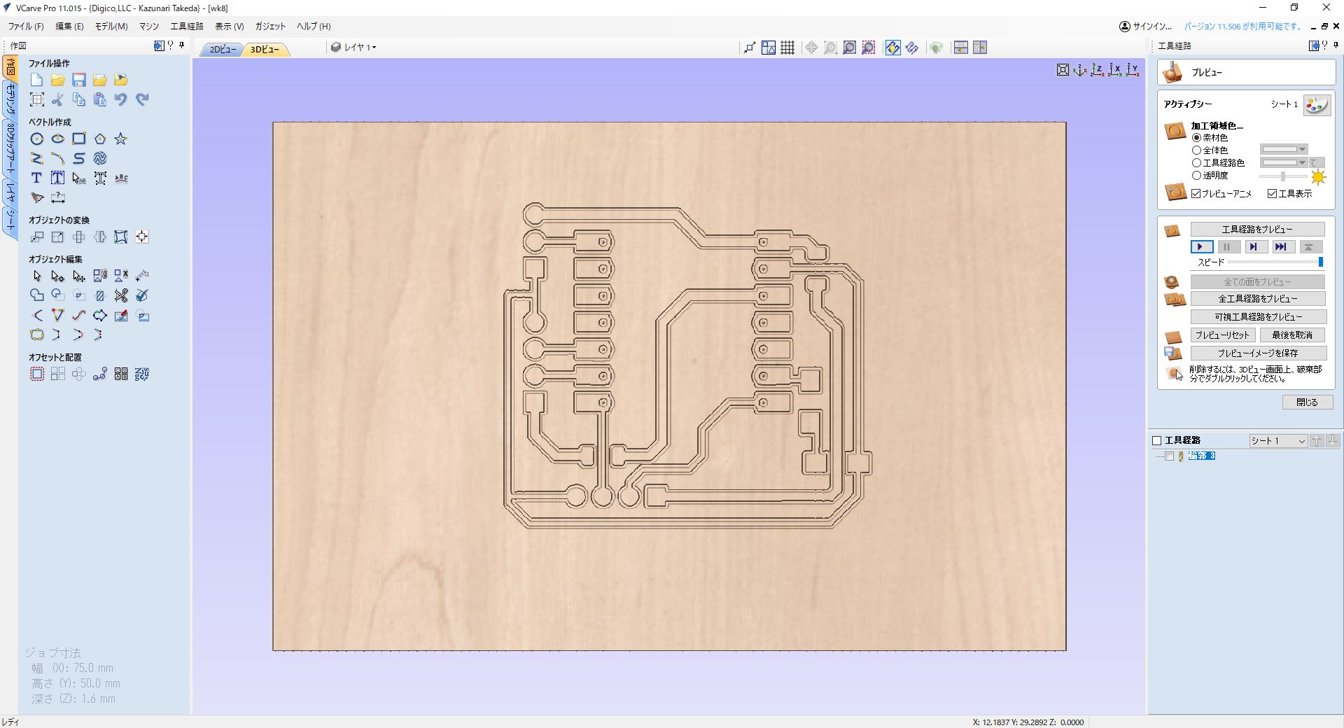
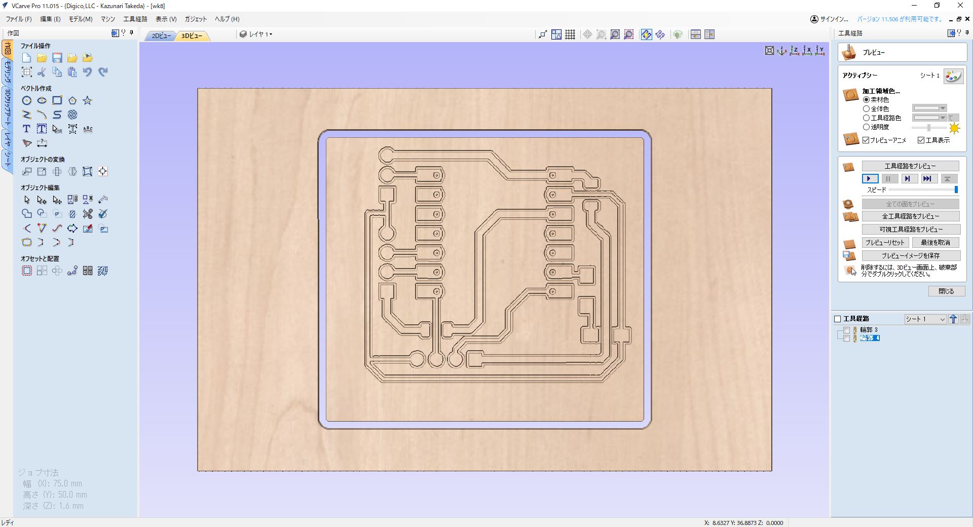
- Completed pattern cut settings, and I can see the image of the milling.
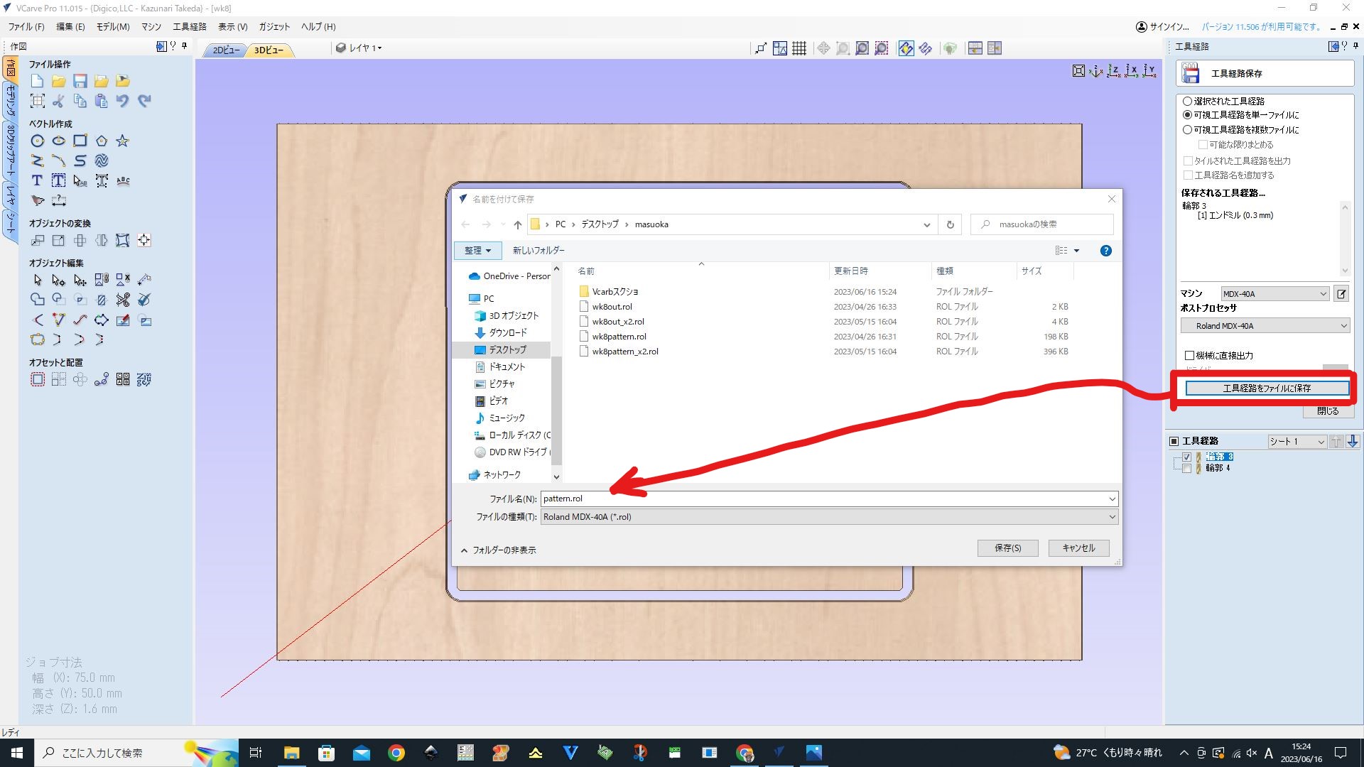
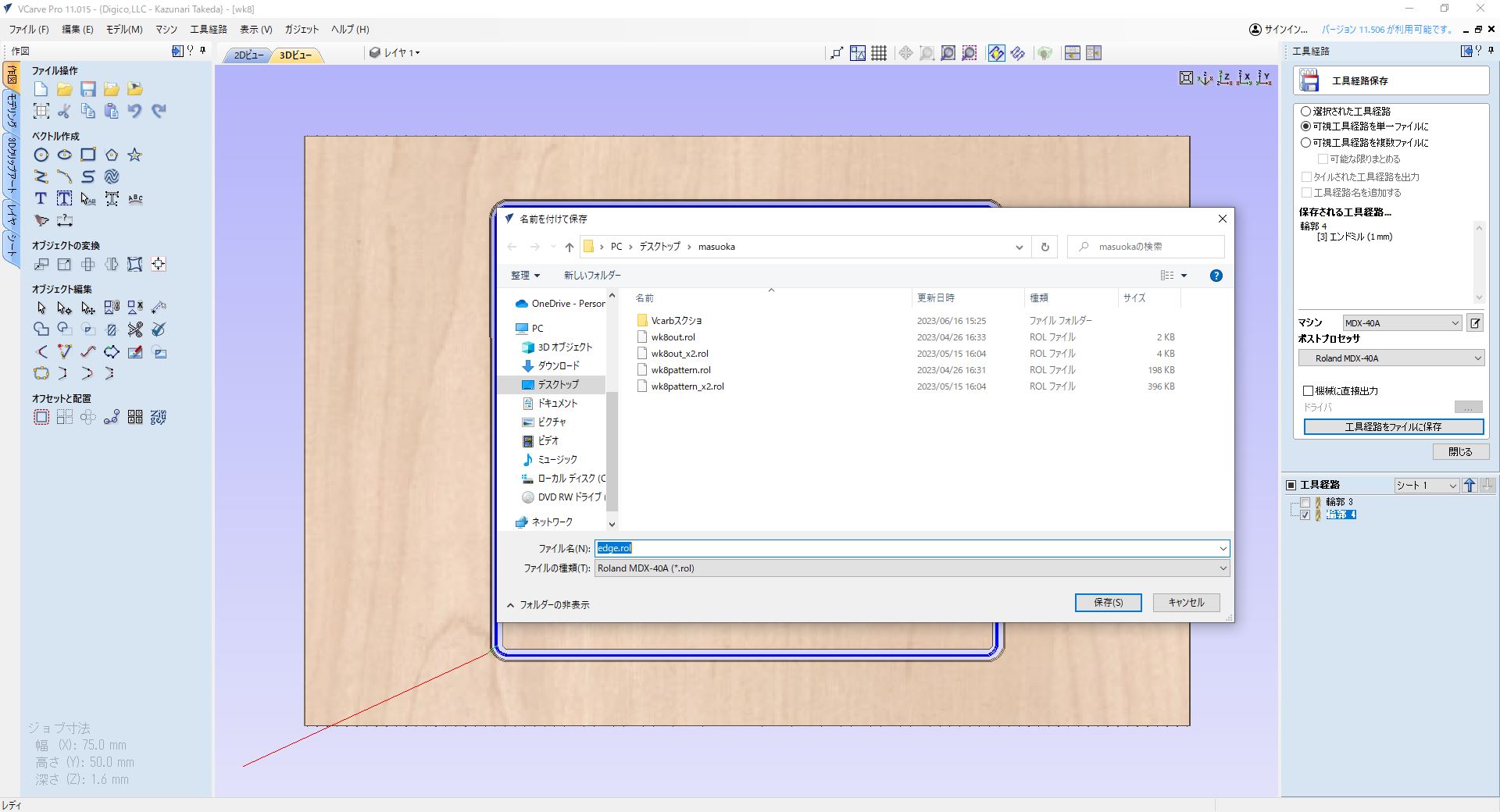
- Export .rol file (original file)
Edge
- Select only edge line for setting. Then start settings in the tool path window.
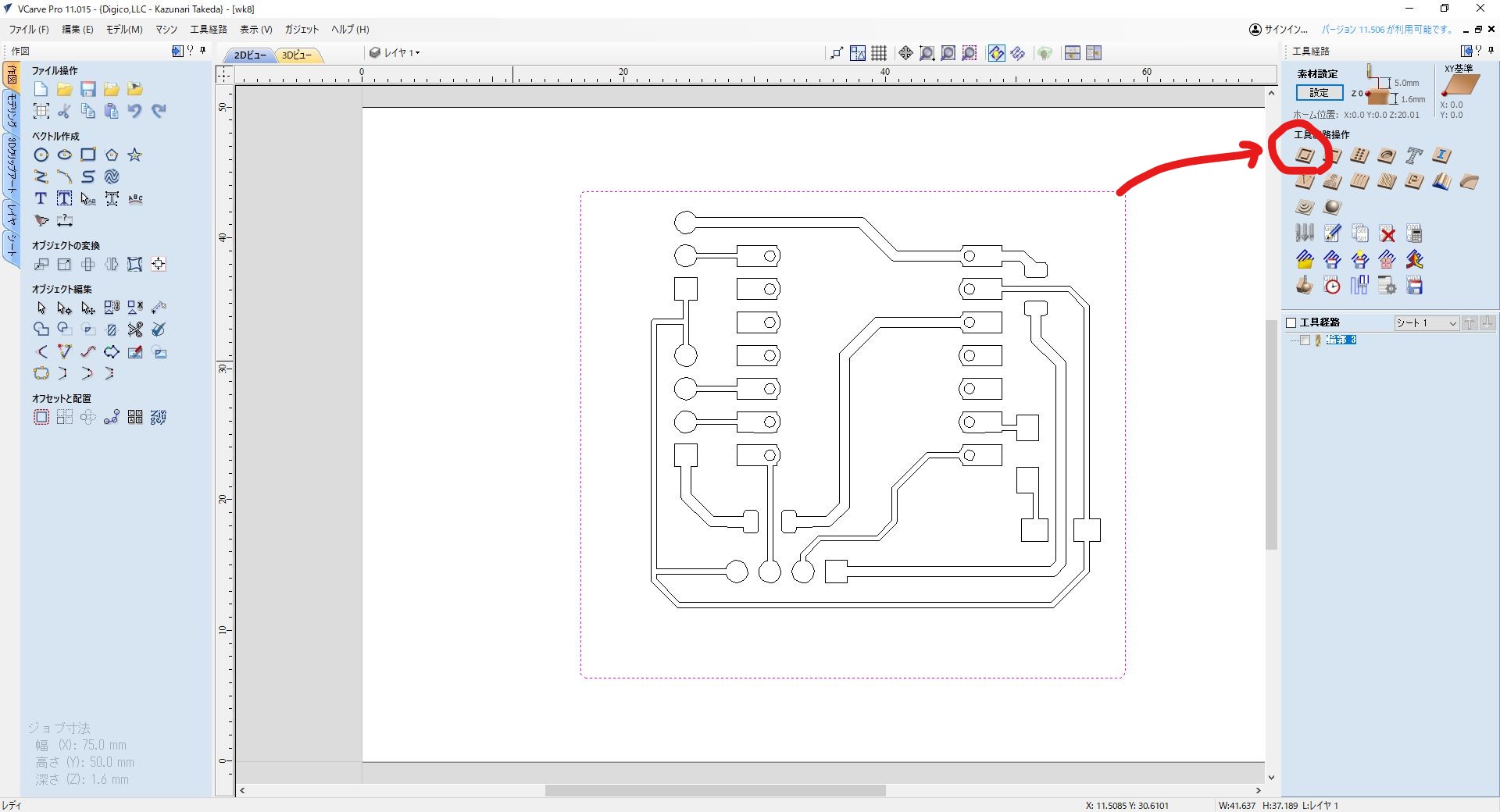
- "Contour" cut settings for edge. Select "Contour" -> "Tool" window to change the tool parameters
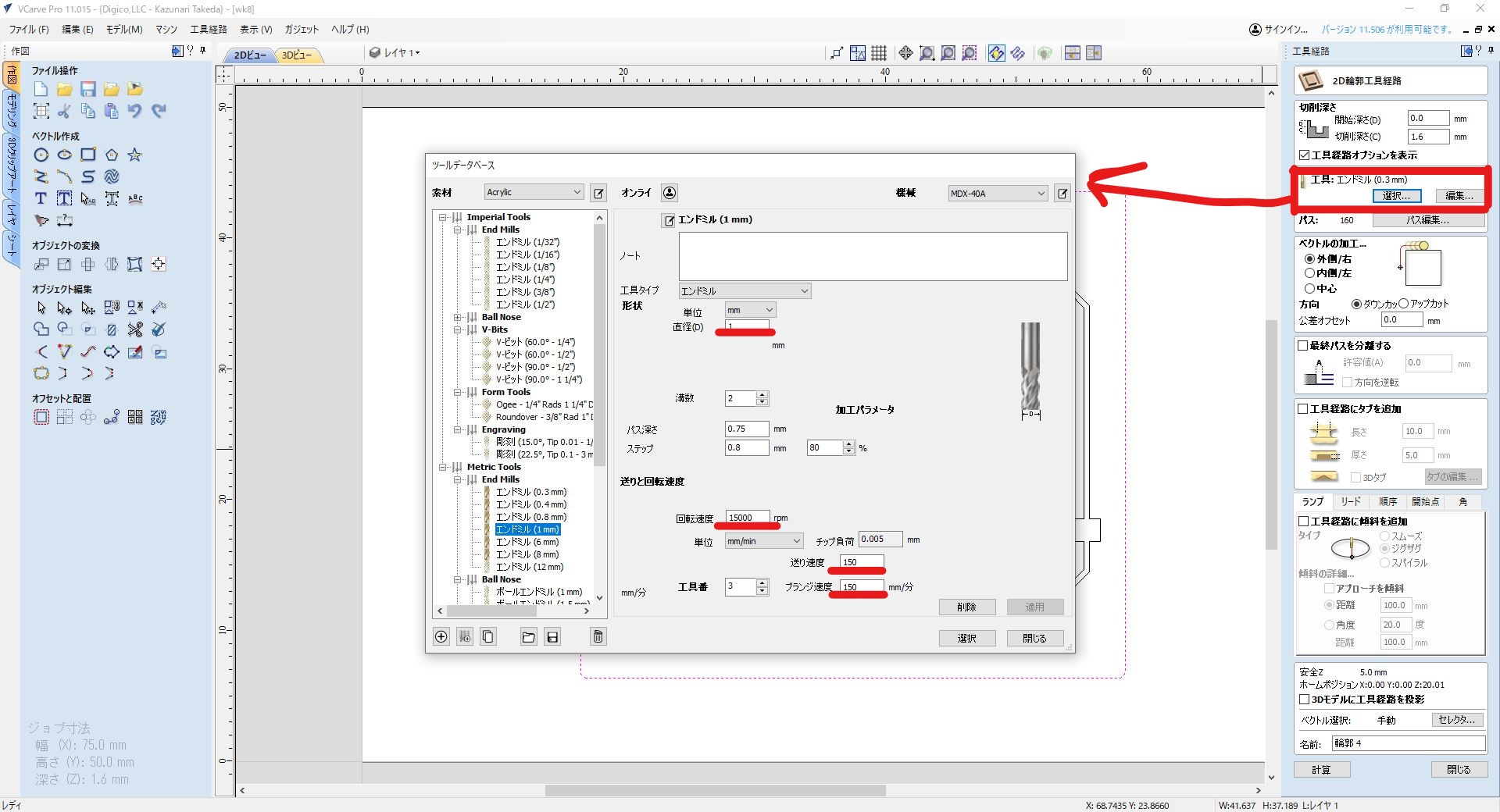
- end mill size: 1mm
- cut speed 150 mm/min
- Number of path and cut depth setting.
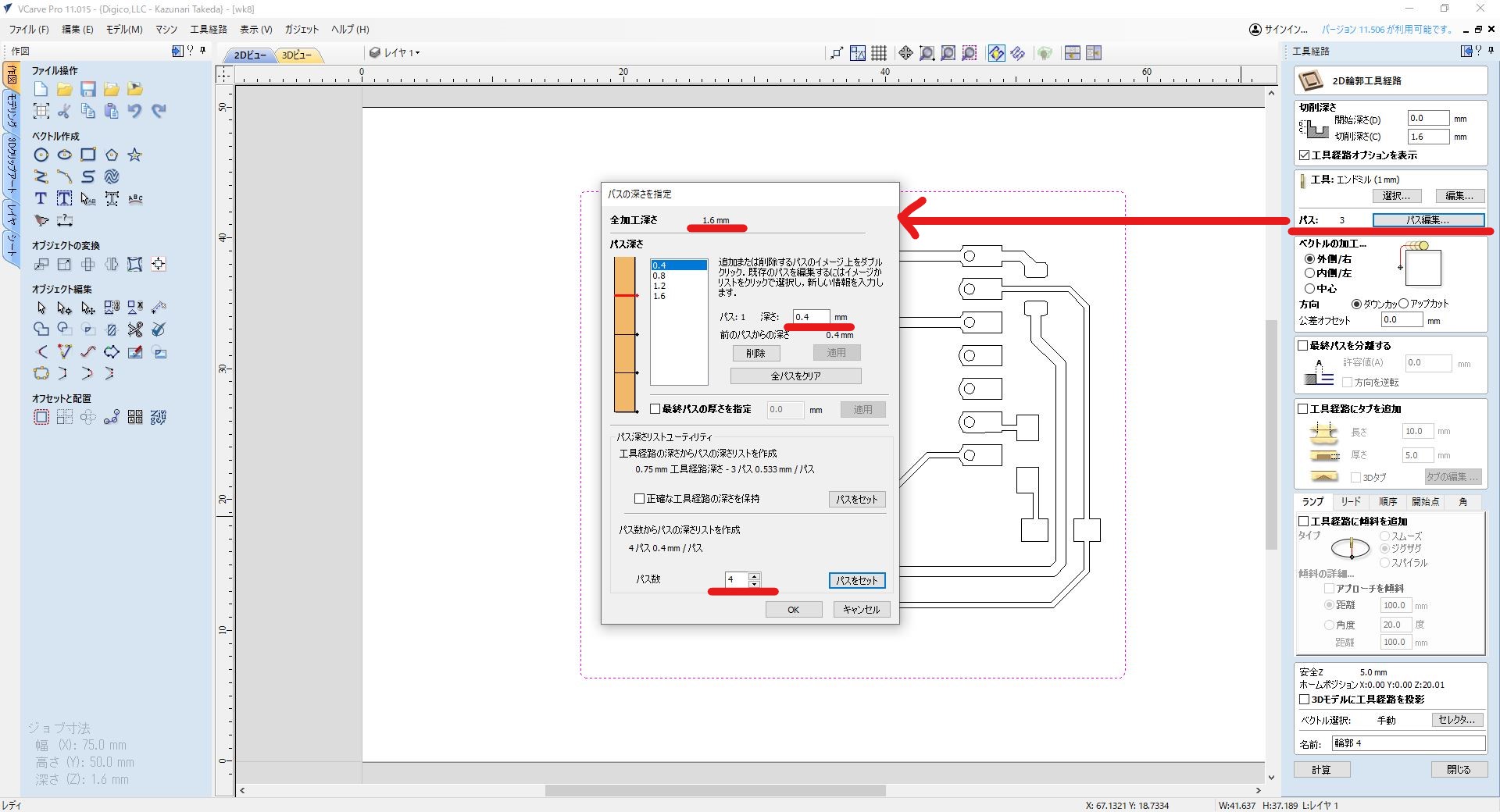
Settings as follows;- cut depth 0.4mm
- Number of cut 4
- Completed pattern cut settings, and I can see the image of the milling.
- Export .rol file (original file)
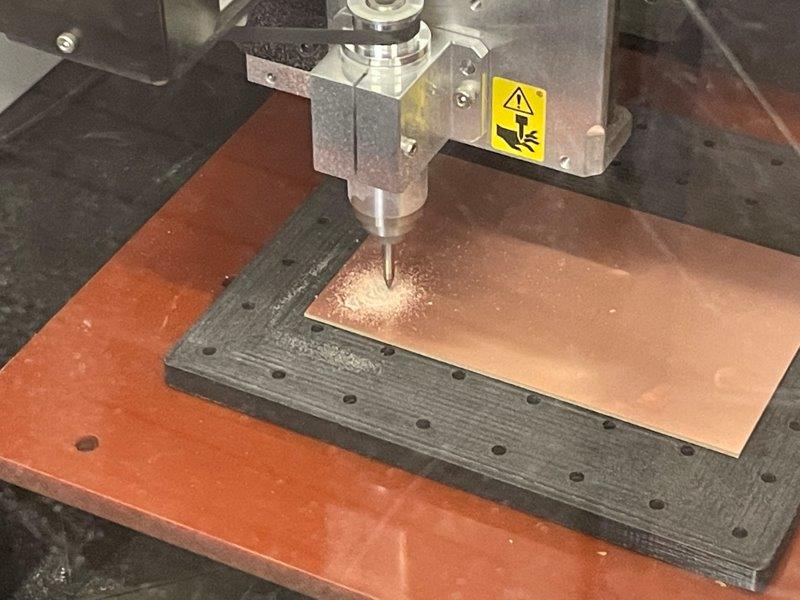
3 Milling with Roland MDX-40A
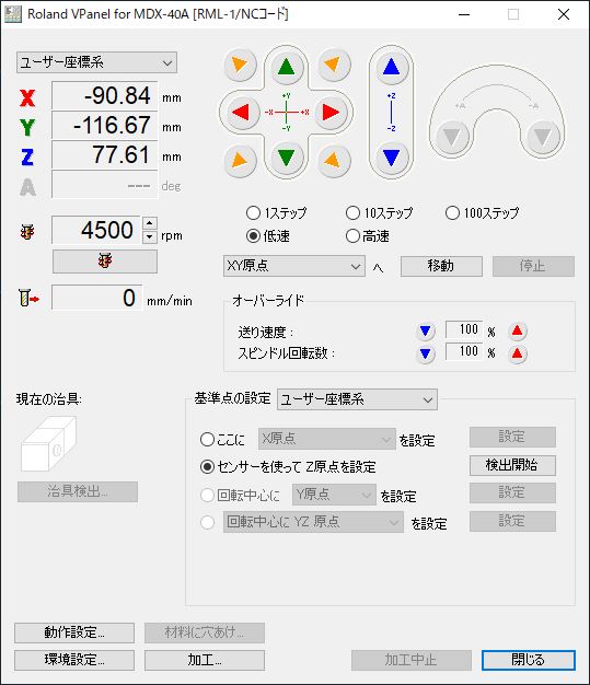
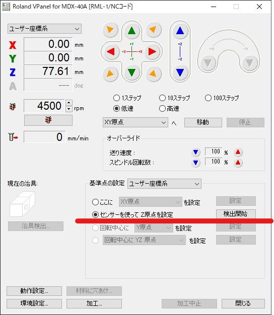
- Controlling software "Roland VPanel". I can operate the software with the machine being connected the PC and power on.
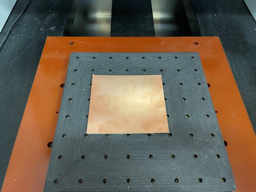
- Put the new board on with sticky tape. So that the board is fixed during the work.
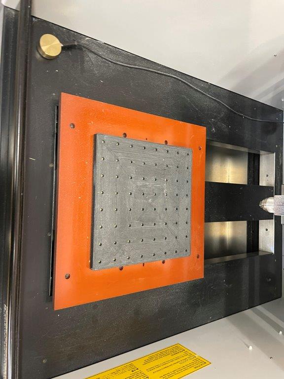
- Set end mill (0. 3mm for pattern, 1mm for edge)
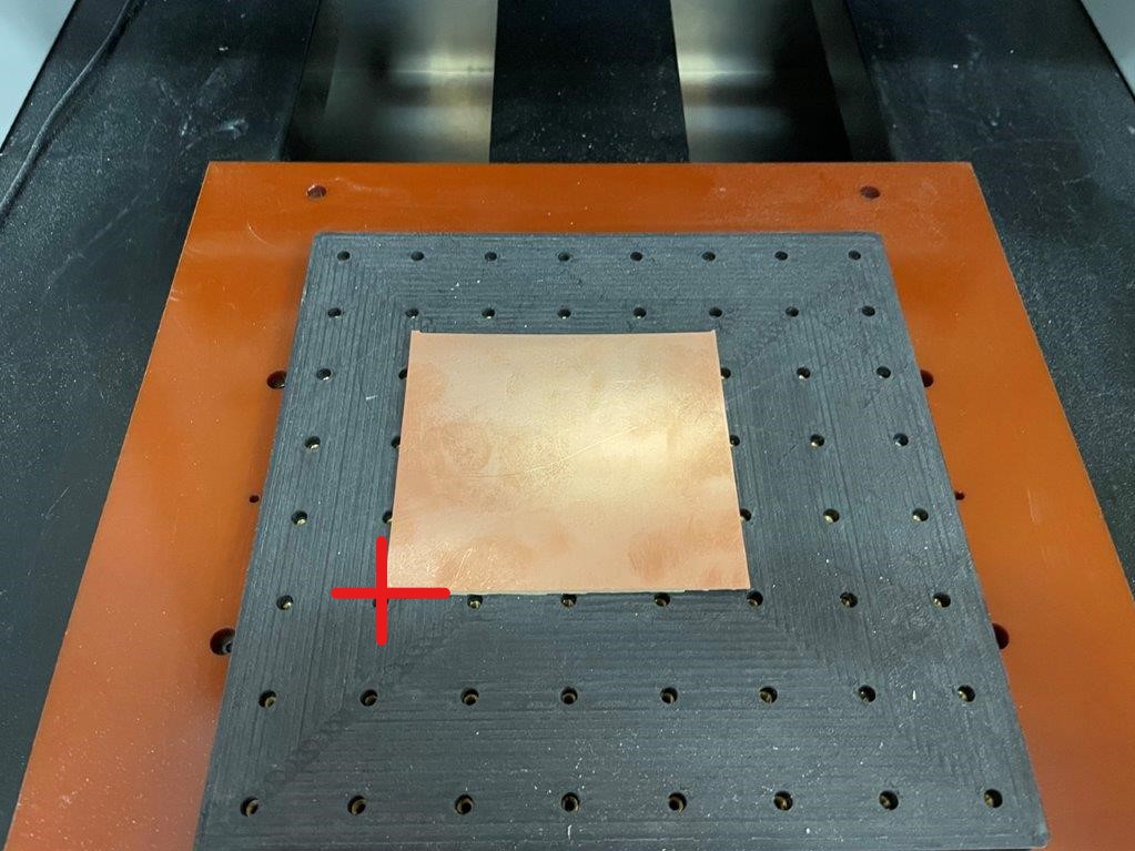
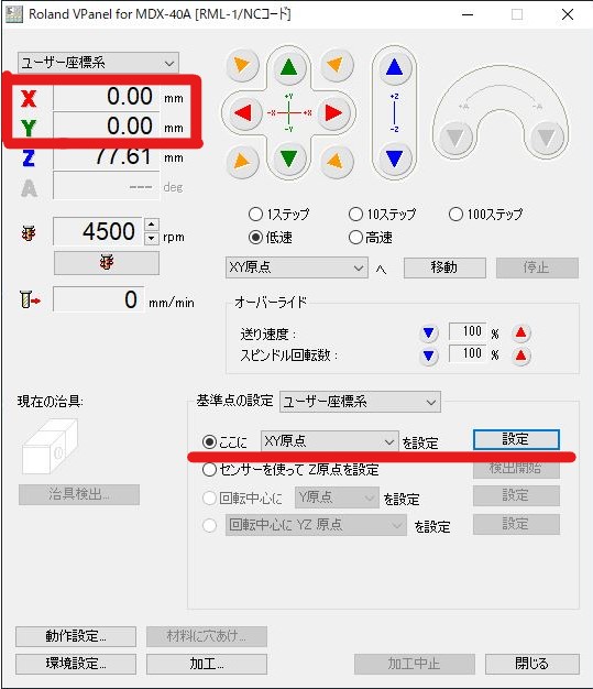
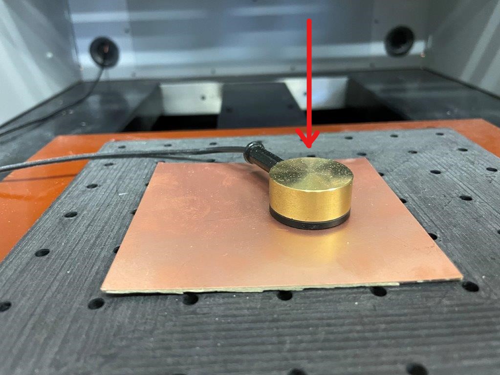
- Bring the spindle by clicking triangles (red for x, green for y) to the left bottom edge of the board on the stage. Then set xy origin.
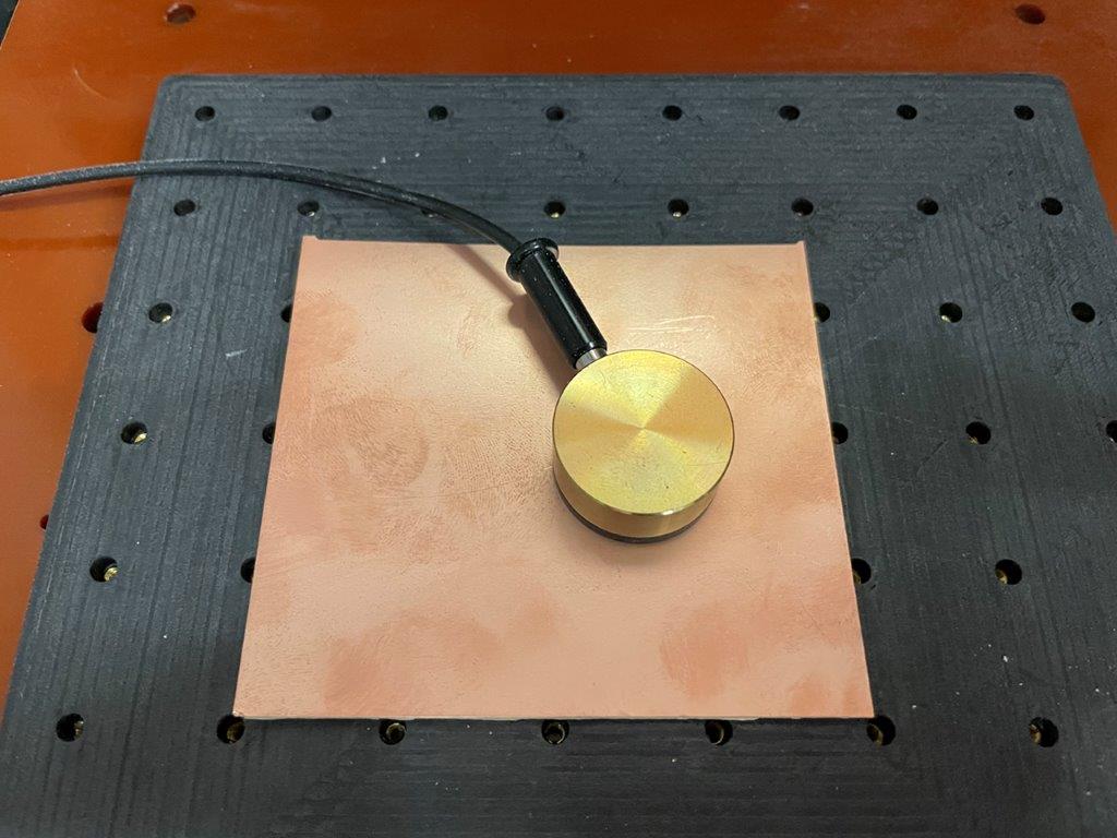
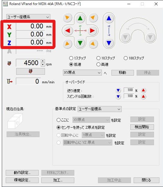
- For setting z=0, put the touch sensor on the board.
And start z=0 detection on VPanel
- Origin setting complete
- Then import .rol file to work start
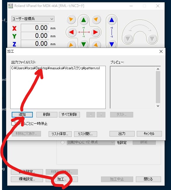
- Milling start
4 Soldering
-
I learned theory of soldering, but this is 100% manual skill. It made big difference between what I thought and what my hand did.
-
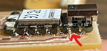
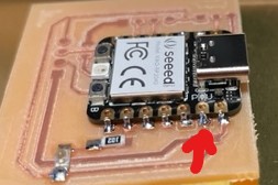
This looks good from above view, but from side I saw the LED is not on the surface of PCB.
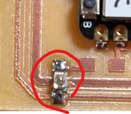
- -> This might be because I did not keep the LED touch down to the PCB while soldering. I must keep it as below.
- -> This might be because I did not keep the LED touch down to the PCB while soldering. I must keep it as below.
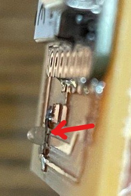
-
This case the solder became ball like shape.
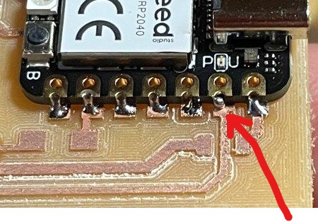
- -> This might be because the heating was not enough. I solder it again and looked better as below;
- -> This might be because the heating was not enough. I solder it again and looked better as below;
- This case solder looks like a horn. I should have kept solder iron longer and melt enough.
-
5 Test interact and communicate
- Used Arduino IDE for editing and uploading code same as week 4
- My board has an LED out of the controller. I tried to blink the LED with below sketch.
void setup() {
    pinMode( 2, OUTPUT );
}
void loop() {
    digitalWrite( 2, HIGH );
    delay(100);
    digitalWrite( 2, LOW );
    delay(300);
}
- Tried to change blinking interval and successfully worked.
6 Thoughts and feelings
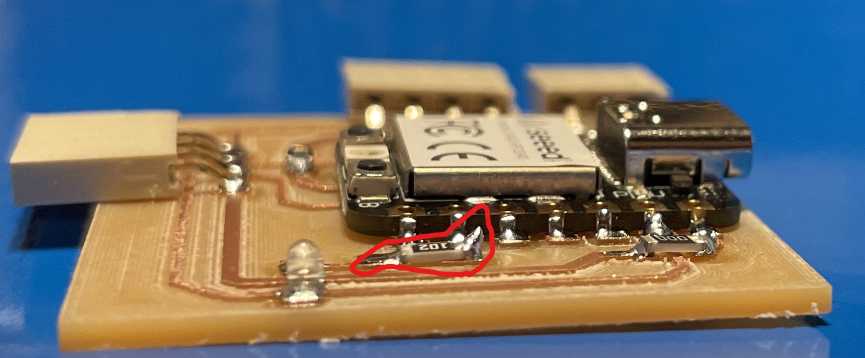
- Soldering is simply difficult, but I managed to make my board and the LED worked as expected.
- Device worked, but soldering looks not good. So I need to keep practicing.
- No debugging around code, continuity test with multimeter was fine, but added solder some as my soldering looked bad.
(end of document)