Week 06 Electronics Design
Group assignment
- Use the test equipment in your lab to observe the operation of a microcontroller circuit board
result -> group site
Thought and feelings
- I learned how to use oscilloscope and when it should be used.
- Oscilloscope is used especially for debugging;
- To know the device is working as expected by checking Voltage and Time. For example the pulse is generated in oscilloscope but the LED is not blinking, then I know the program and the controller is ok but something wrong with the LED or cable.
- As this oscilloscope has 4 channels I can use the checking of the combination of devices by watching 4 waves at the same time.
- This is good start to know how to debugging.
- Some questions are not solved yet. I will study more for coming debugging.
- Why LOW signal was longer than programed while HIGH signal was the same as programed?
- Why the analog wave shape was not stable or I could not adjust properly?
Individual assignment
- Design a development board to interact and communicate with an embedded microcontroller
Result
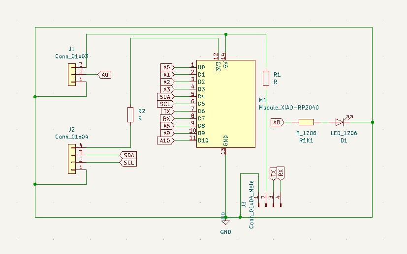
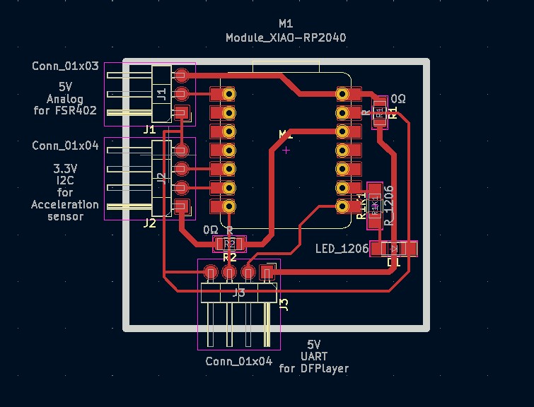
- I designed a board for 2 sensors and 1 sound device with Kicad.
- Microcontroller is xiao RP2040.
Schematic(original data)
 PCB (original data)
Process to the result
-
Start a new project file
-
Add symbols I can add a new symbol by clicking "Place" -> "Add symbol"
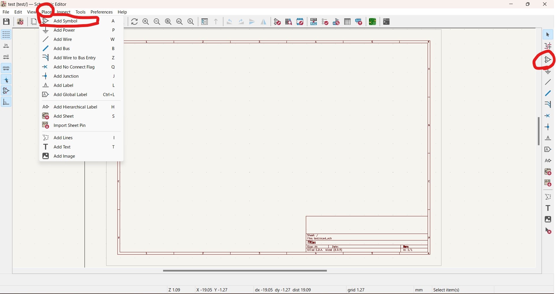
Automatically a window pops up
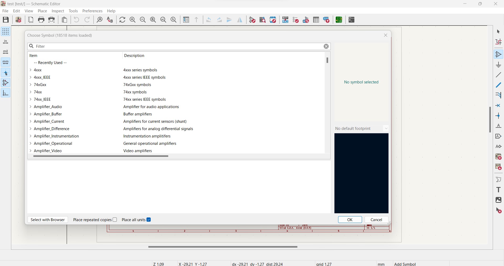
Search by inputting Filter window
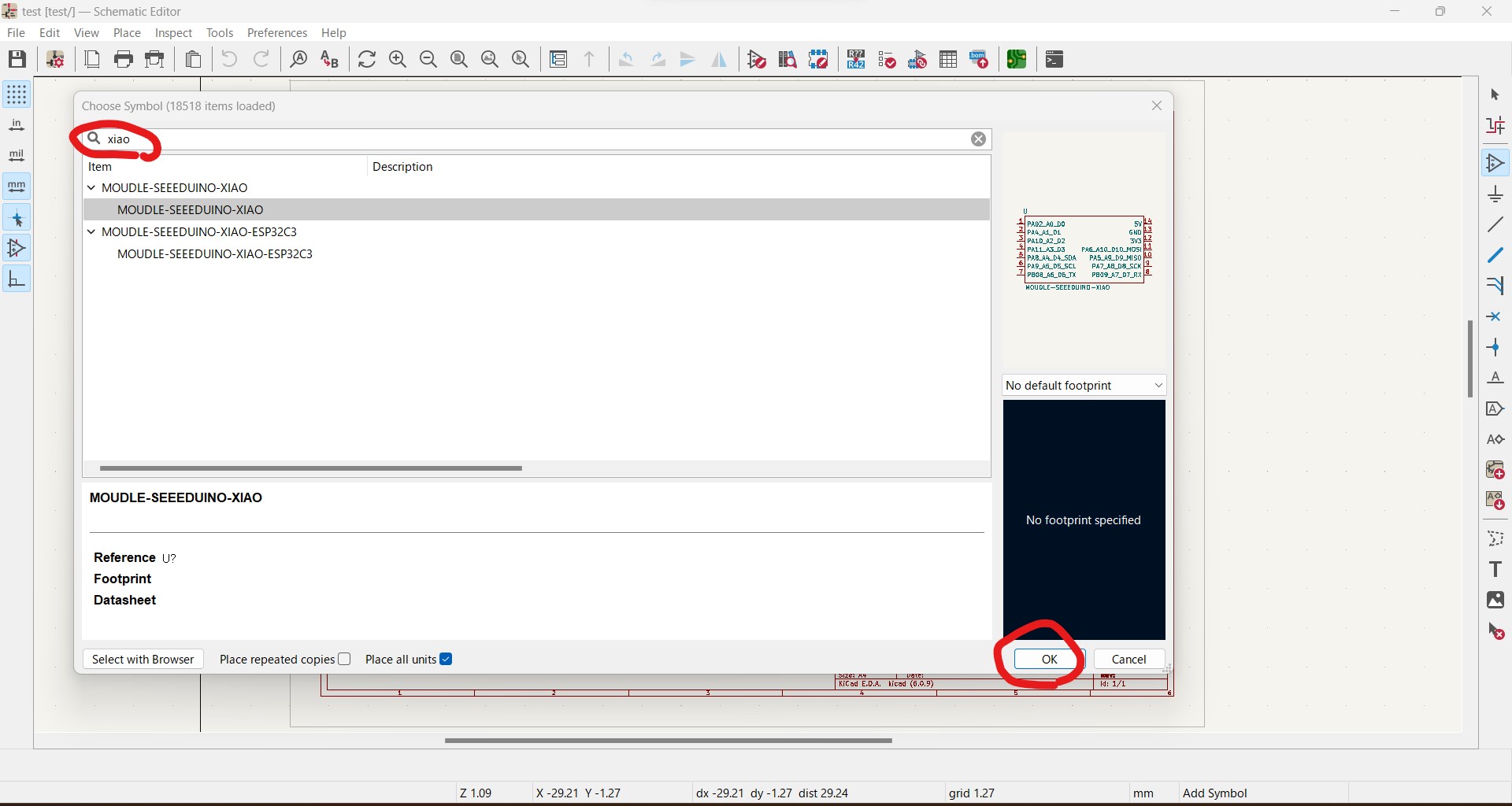
A symbol appeared on the working sheet

If I want to add a symbol but not included in original library, I can add it. For example, my design includes XIAP RP2040, but it was not on the original library then I refer this site and downloaded the library file. -
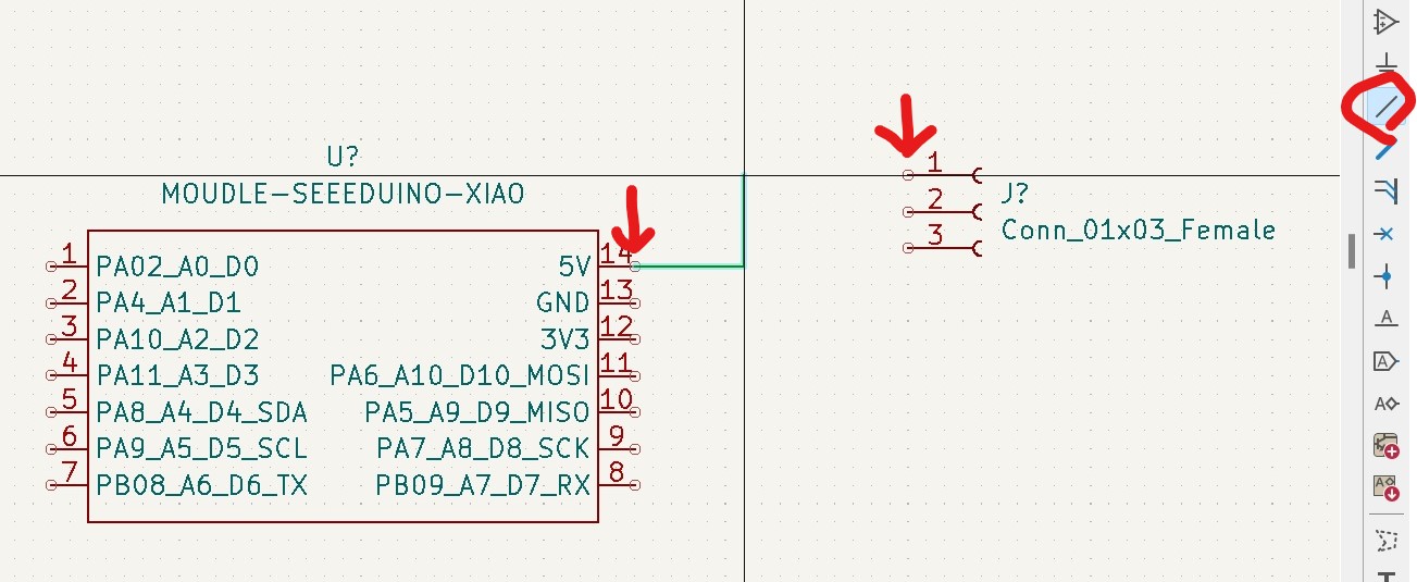
Draw lines
I can draw line (pattern) by clicking "Place" -> "Add Wire"
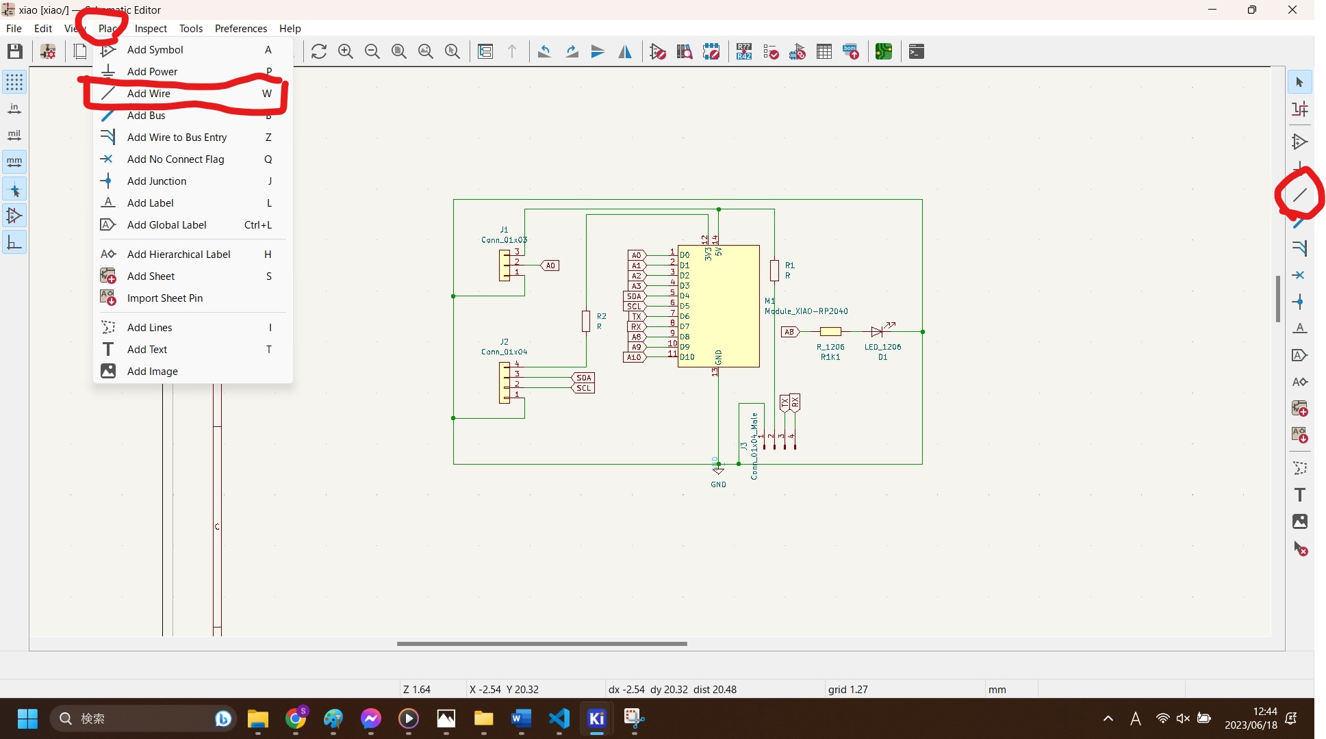
Click start and goal of the line to draw it
-
Checking or change footprints
Once all symbols are allocated on the sheet, I need to link the symbols and footprints by "Run footprint assignment tool" and find the appropriate footprint for each symbol.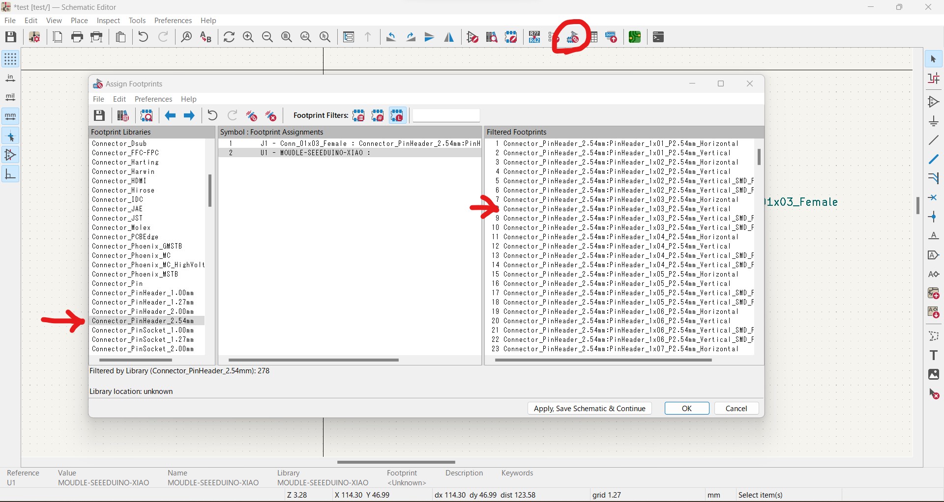
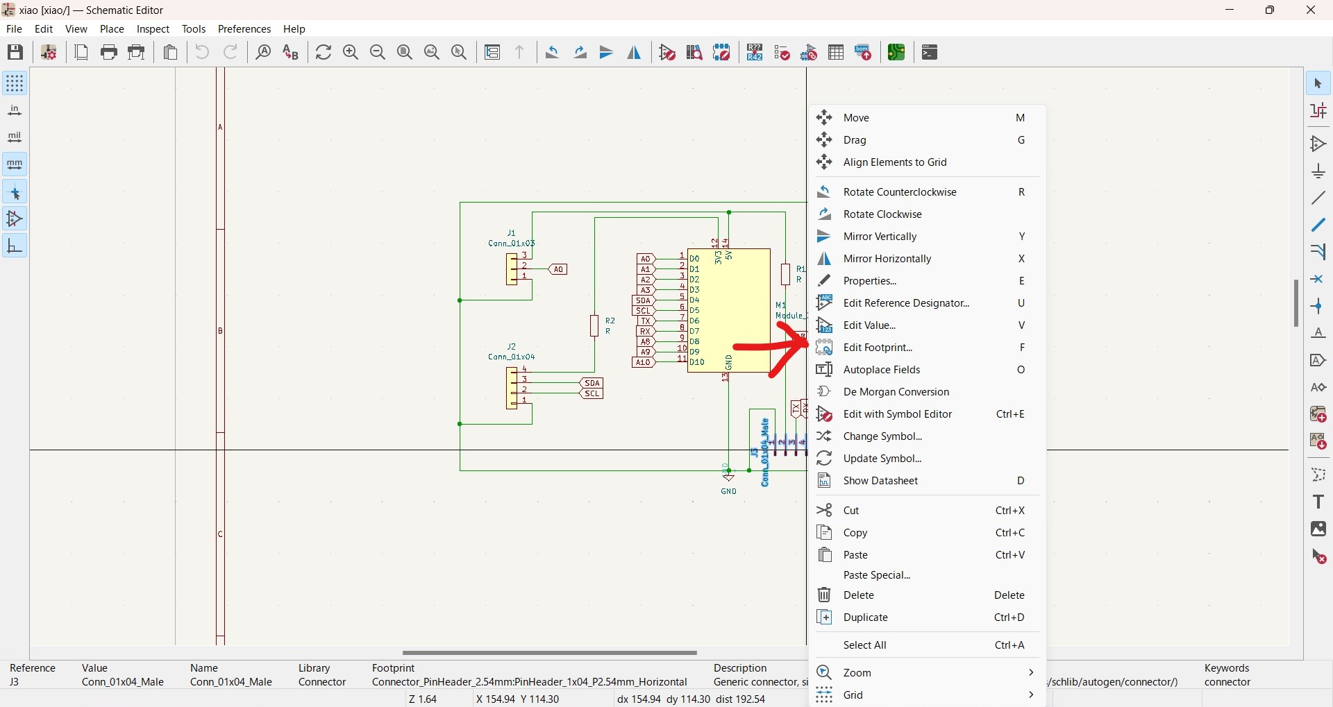
Once footprint is assigned, I can check it by "Right click" -> "Edit footprint"
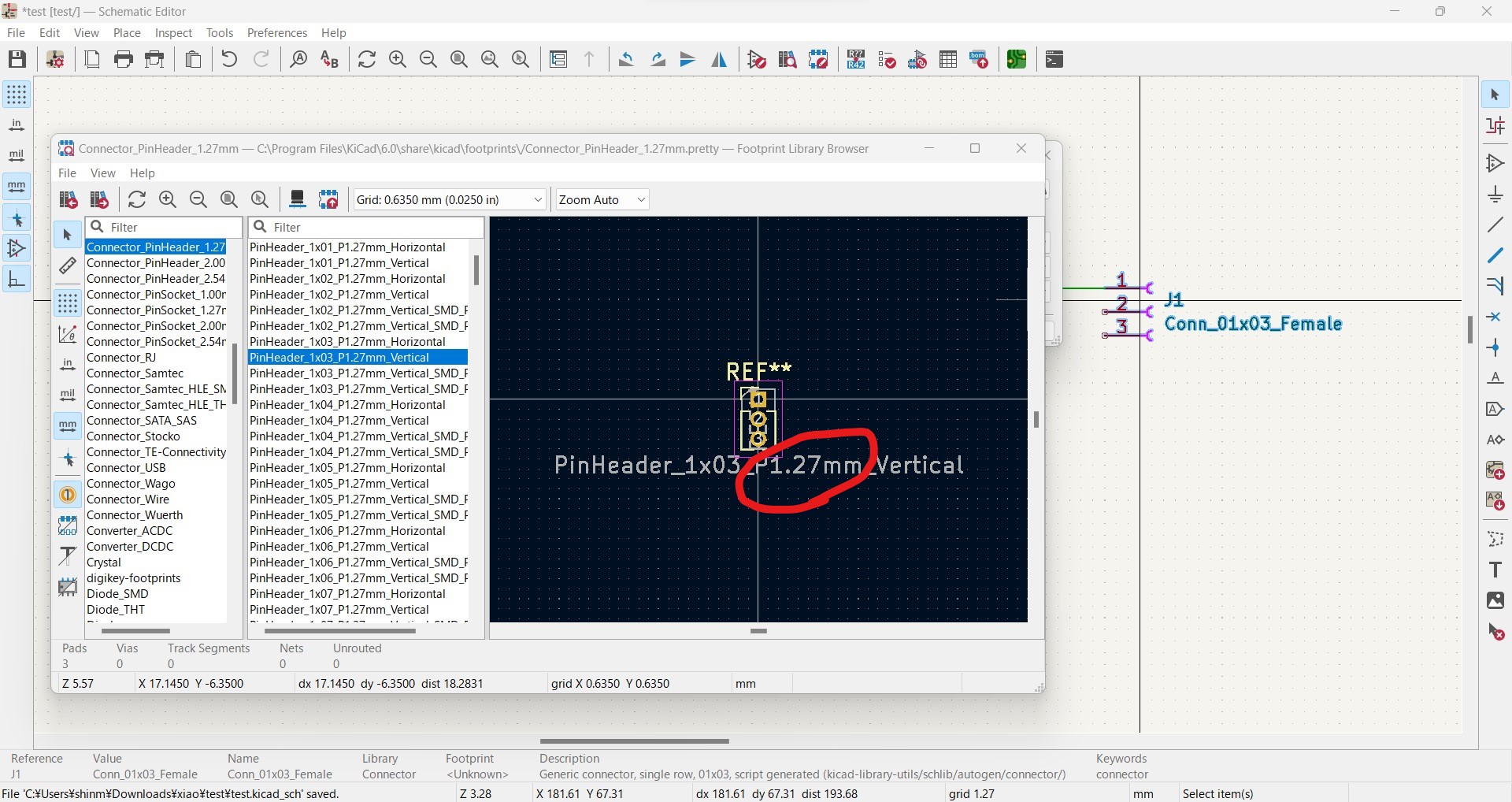
"Edit Footprint Field" window pops up, and I can see actual footprint

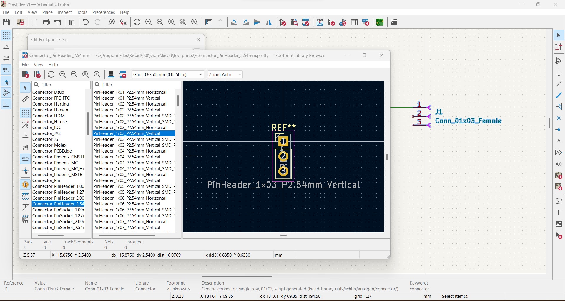
I can choose other footprint with this window
-
ERC (Electrical Rule Check) Once schematic design and annotation complete, I can run ERC.
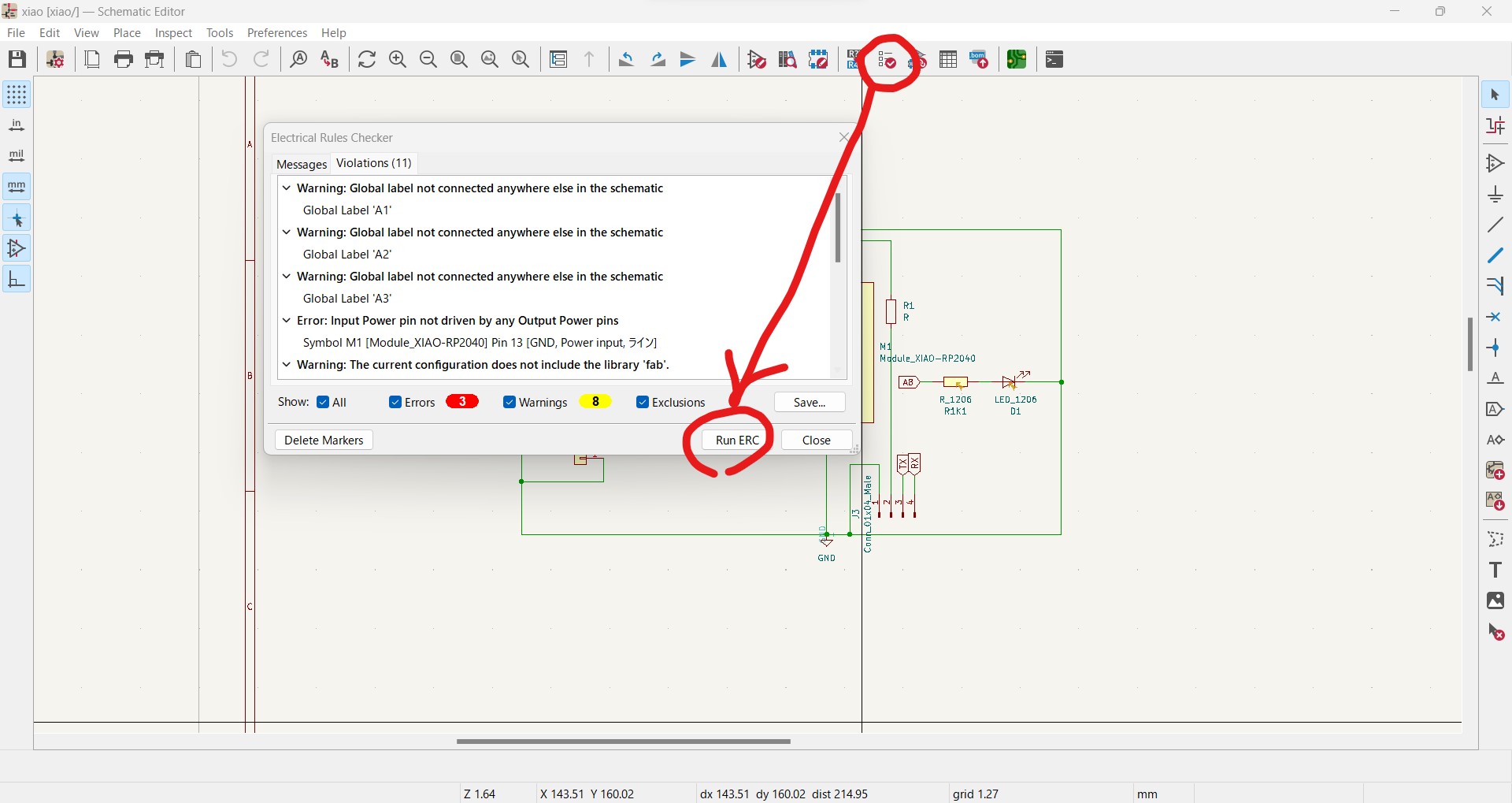
ERC detects something if the design was wrong by electrical theory of view. - Update PCB from Schematic
By clicking "Tools" -> "Update PCB from Schematic", the design changed into PCB


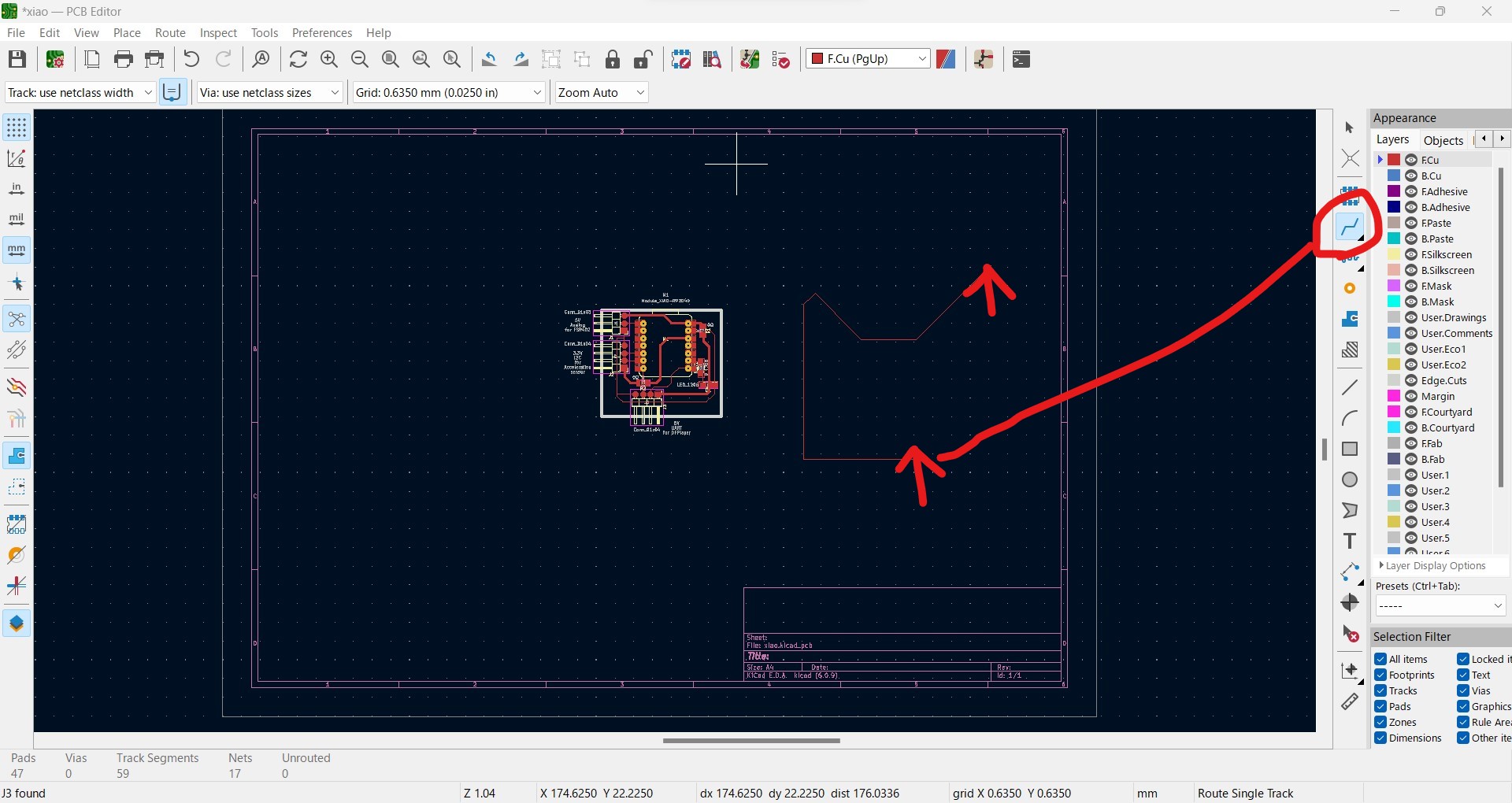
Then I move symbols and draw route tracks to create actual board design - Design PCB
I need to draw cable line (tracks) by "Route tracks" tool
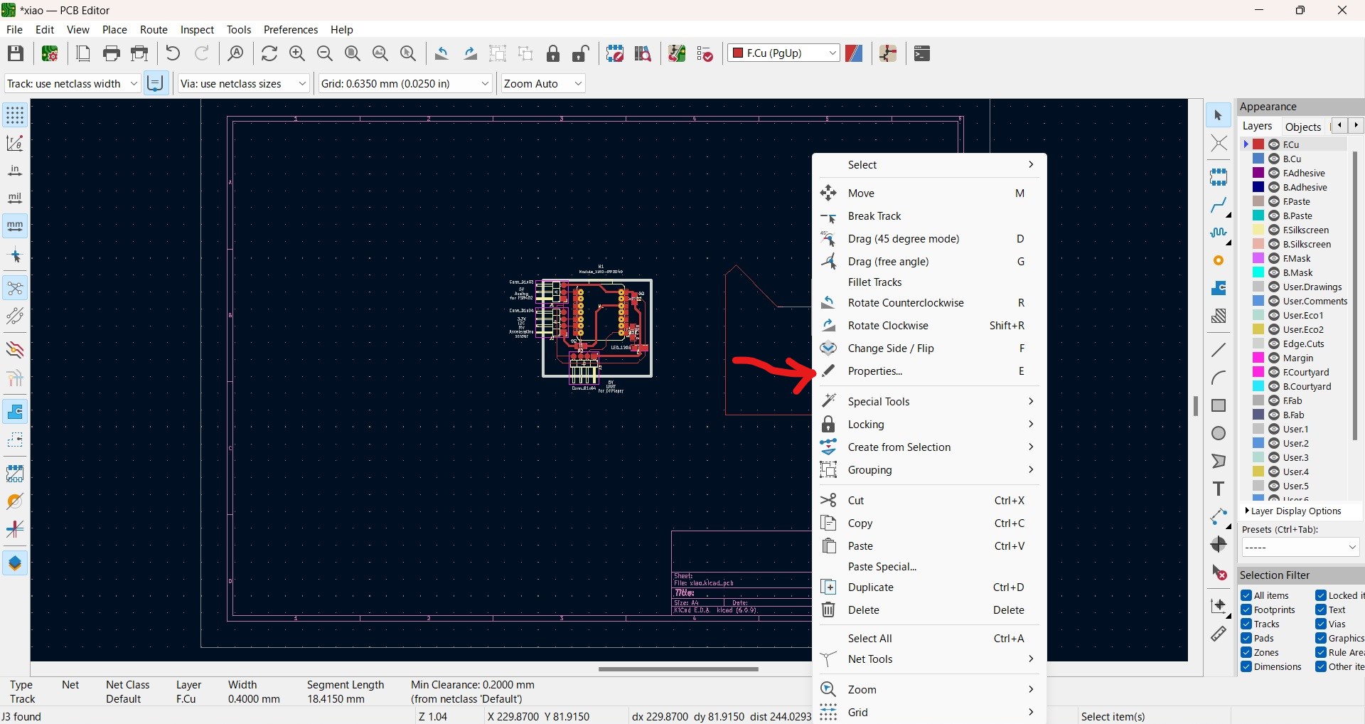
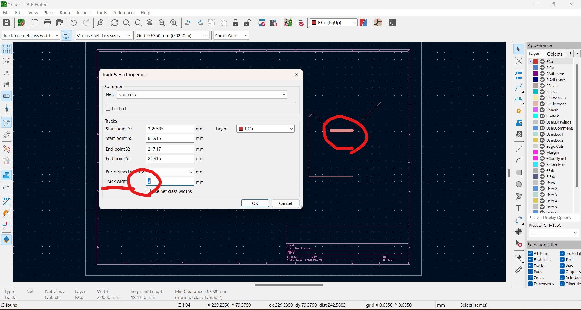
I can change the track width by "right click" -> "Properties" -> "Track width"

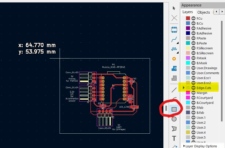
- Drawing edgecut
There is shape drawing tool (rectangular etc.), but important thing is to choose appropriate layer. For edgecut, I choose "Edge.Cuts" layer and draw edgecut line.
Thoughts and feelings
- The first use of Kicad, took long hours for new tool as usual. Especially when I draw a line, it moves unexpectedly.

- This time I stuck 2 times for drawing PCB.
- At first I used horizontal connectors, it caused many cross lines so I could not draw anything. Instructor advised that if I use vertical one the connecting part is not on the board (standing) so the line can go straight for next device.
- Still there are 2 crossing points. And this was cleared by using 0 resistors to make bridges.
- I learnt that to make PCB simple, I need to know physical shape of connectors and other devices. And also do not hesitate using 0 resistors to make it simple.
- At this moment I enjoyed line arranging as a puzzle, hope this feeling continues.
(end of document)