7. Electronics design
Week 07 · 2023.03.01-2023.03.08
This week I worked on designing a PCB by understanding how to work schematic design and then pcb design through a specific EDA CAD.
- [x] Linked to the group assignment page Fablab Ciudad de México Page
- [x] Documented what you have learned in electronics design
- [x] Explained problems and how you fixed them.
- [x] Included original design files (Eagle, KiCad, etc.)
- [x] Included a ‘hero shot’
KiCAD choice and installation
There are many options for PCB design, through the experience of the members of fabacademy you can tell that many used to work on Eagle, now part of Autodesk Fusion 360. Since the spirit of Fabacademy is to support, learn from and work in open source or free tools, KiCAD has become -apparently- the standard to work on.
We had a tutorial sesion with Rico Banthatham about SVG to PCB tool in saturday open time, but we where advised that in order to fullfill the current assessment it was necessary to use other options such as Eagle or KiCAD, since SVG to PCB doesn’t have schematic view or editor. According to one instructor the main advantage of KiCAD is that KiCAD has very useful keyboard shortcuts, therefore it seems to be the best tool. (I found out that in fact the shortcuts are very useful, A · for adding new components, R · for rotating, M · for moving, X · for drawing tracks and alt + 3 · for the 3D viewer, are my most used)
For setting things up:
1. Download Kicad, and choose the right system and bit version. In my case 7.0 version for Windows 64 bits. (kicad-7.0.0-x86_64)
2. It is usually recommended to right click and run the installer as administrator
Then for adding the fabacademy components:
1. Clone or download this repository. You may rename the directory to fab
2. Store it in a safe place such as ~/kicad/libraries or C:/kicad/libraries
3. Run KiCad or open a KiCad .pro file
4. Go to “Preferences / Manage Symbol Libraries” and add fab.kicad_sym as symbol library
5. Go to “Preferences / Manage Footprint Libraries” and add fab.pretty as footprint library
6. Go to “Preferences / Configure Paths” and add variable named FAB that points to the installation directory of the fab library, such as ~/kicad/libraries/fab or C:/kicad/libraries/fab. This will enable the custom 3D shapes to be found. The 3D shapes project has just started and most of them have to be populated still
In the schedule page for fabacademy 2023 the BOM plugin is listed for it to be taken in account and installing it, since it mentions that is usefull for complex electronics I haven’t found so far the need for installing it.
KiCAD start a project
Before starting we had a splash intro to KiCAD with our instructor locally, then I followed the intro documentation and after I found a tutorial recommended by a previous student of fabacademy which helped so much more. This is another (video quick tutorial from Fabacademy)[http://academy.cba.mit.edu/classes/electronics_design/KiCad.mp4] for KiCAD.
Start project by openning KiCAD and creating a New Project.
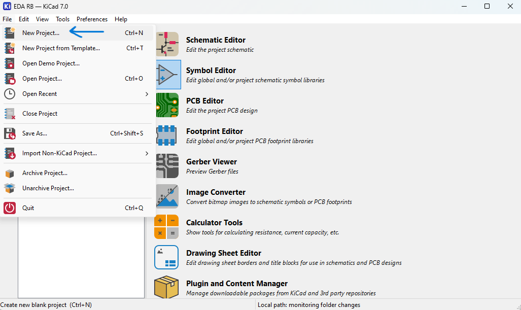
KiCAD works as a set of bonded programs, so first it is advisable to go through the schematic editor.
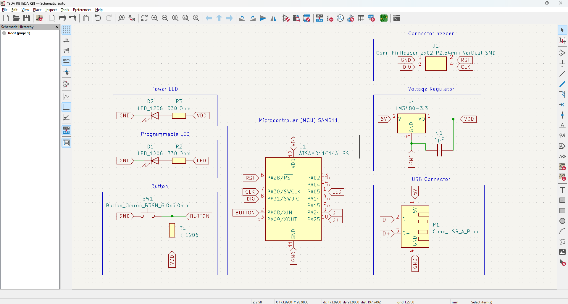
Take in account that you should have already a preselected set of components to incorporate to your developer board.
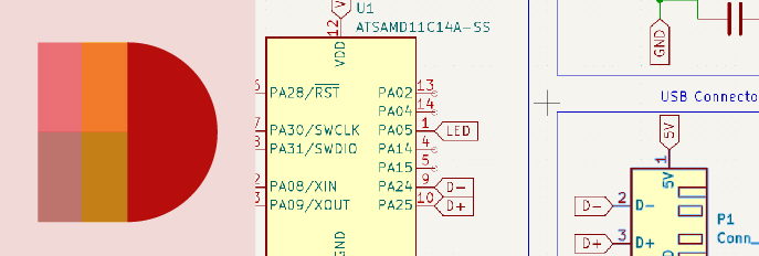
1 Microcontroller (MCU) ATSAMD11C14A-S
2 LEDs
2 330 Ohm Resistors
1 1k Ohm Resistor
1 Button Omron B3SN
1 Connector Pin Header 2 x 02 P 2.54 Vertical SMD
1 Voltage Regulator LM3480 100mA
1 Capacitor 1μF
Every component is selected under an architecture 1206 and is SMD, o “Surface Mounted Device”.
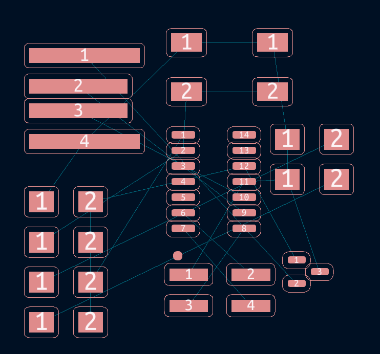
KiCAD Schematic editor
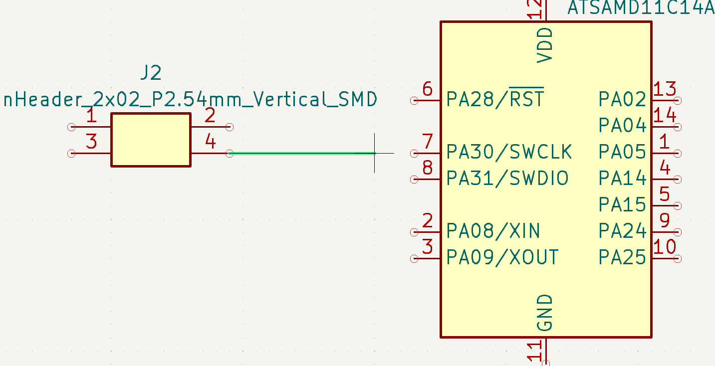
Since Fablab CDMX has plenty of SAMD11 we were adviced to start from there. Then I searched for previous generations and found that Fablab BCN used them last year, then I went through the documentation of some of the students to checkout the components used and made some adjustements, such as changing micro USB for regular USB A connector.
Already in the schematic editor, you start by adding the components, by clicking the add component symbol (third from top to bottom in the right menu) or you can click ‘A’.
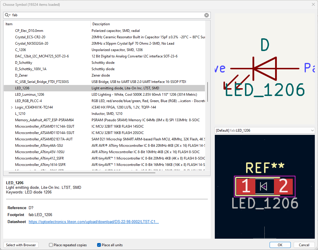
You may find most of the components needed for this board under the fab library within KiCAD add component menu section.
After you add all the components you can start connecting them, by drawing connections with the ‘add a wire’ tool (fifth from top to bottom in the right menu) or you can click ‘W’.
Click on the circle of the connector of one component and then click on the circle of the connector of another component
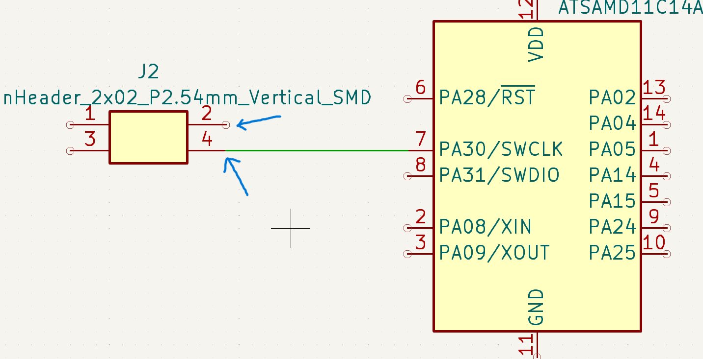
You will know there are connected because the small circle of the connector is gone
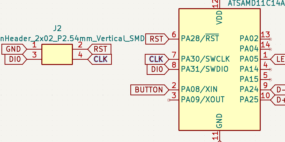
Another way of connecting components, is with tags, this is done by adding global tags, with the icon for such purpose with the same shape as the tags in the previews image, or by clicking ctrl + ‘L’. You must place the tag with the same name at the end of every connector you want to wire.
After you have all the connections worked out, you may add text and ‘grouping boxes’ so it is more understandable the schematic design of your developer board.
KiCAD PCB Editor
After you have added (by double clicking) the right values for resistors and capacitors, have double checked connections, and are happy with the schematic design, you open de PCB editor.
Then you may click on update PCB with changes made on schematic button in the upper menu to put all the components derived from the schematic design here, according to their (copper) footprints.
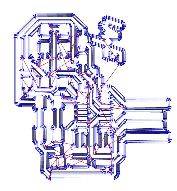
The components appear with an ‘air’ wiring for you to resolve how to order the components with the least puzzling, and NO crossing lines.
So then you should order the components according a logic such as:
- USB connector needs to go on one side, and needs to protrude to be connected
- The MCU must have a central location since it may be the most connected component
- The button and the 4 pin connector should be accesible since there will be some manipulating over them
- Resistors connected to LEDs should be very close one to another
- Rotate components and place them with as few crossed ‘air’ (blue hairlines) connections as possible
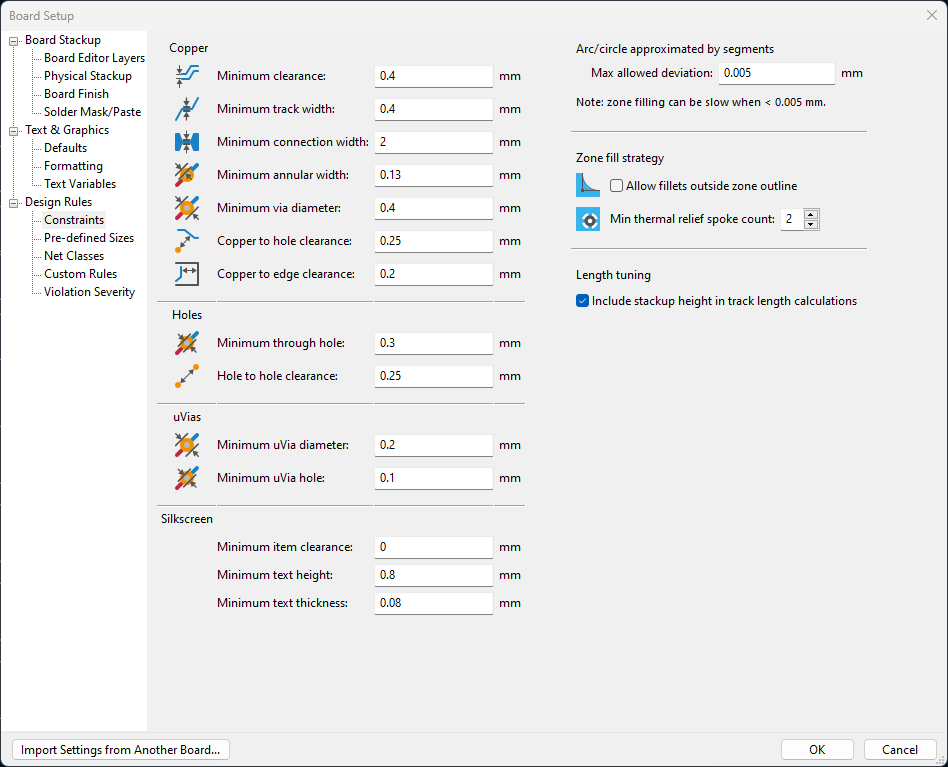
- Set your design rules, according to your fabrication capabilities, such as track width and clearance, in my case 1/64” or 0.4mm (check this with the person in charge of milling or your instructor) –the rest of the design rules I took in account came from the tutorial a previous student recommended which I already mentioned before–
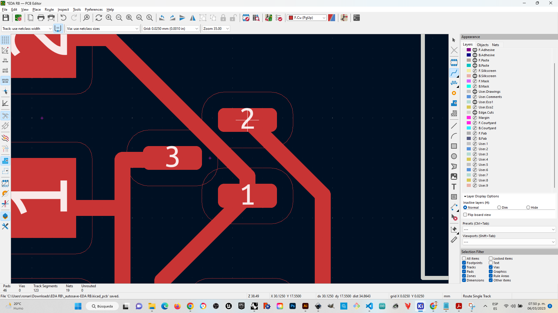
And then the real tracking begins
You can start drawing tracks by pressing the Route Tracks button on the right, or simply by locating the initial connection center and hitting ‘X’ and then the dynamic wiring (with diagonal will start)
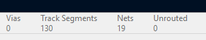
Connect everything until you remain with 0 unrouted
If you are not happy with your tracking connections, you may modify them by clicking-hightlighting-and dragging them, or by erasign portions.
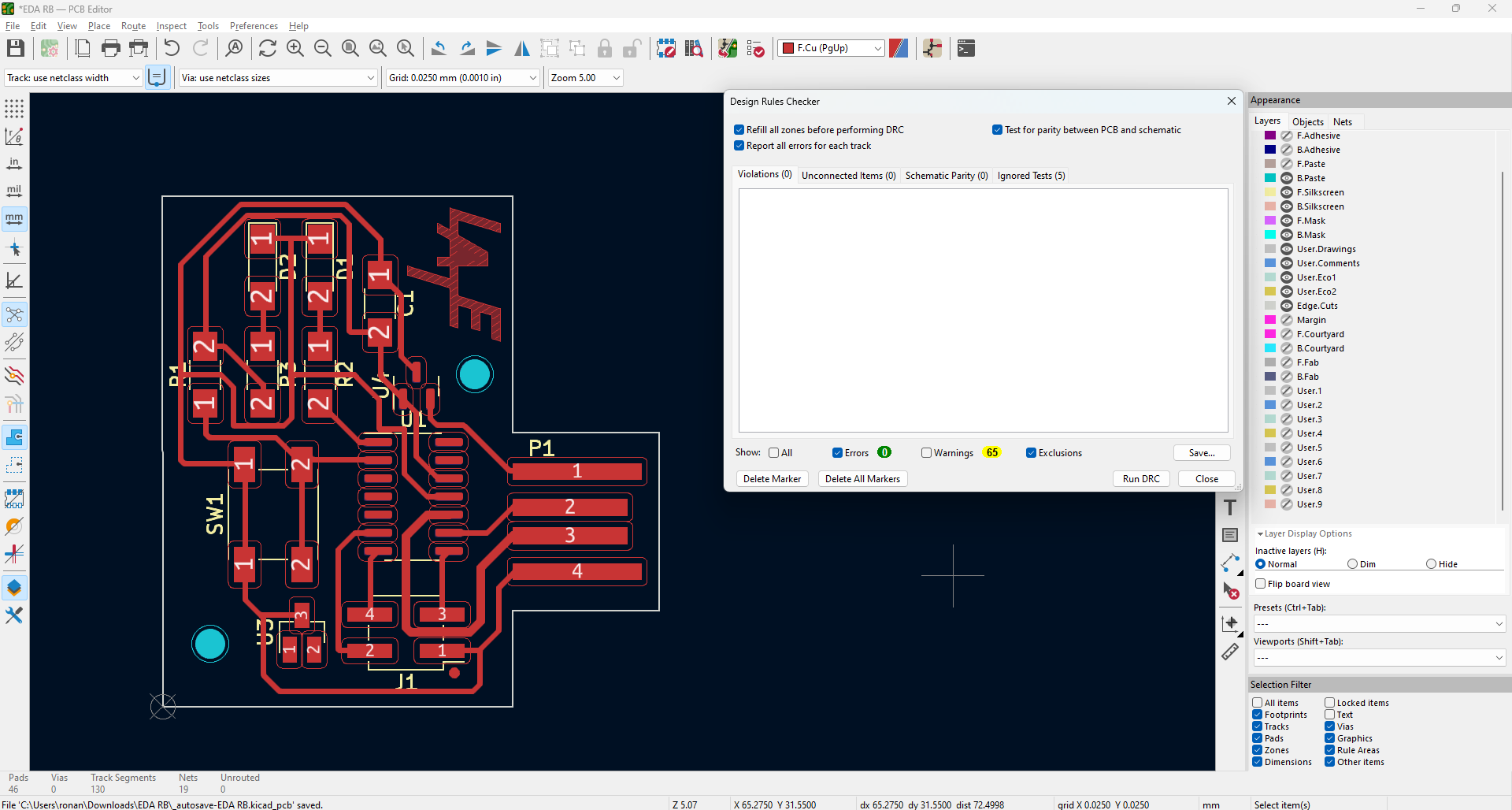
Then you may run the Design Rules Checker, and you will have a better idea of what is wrong.
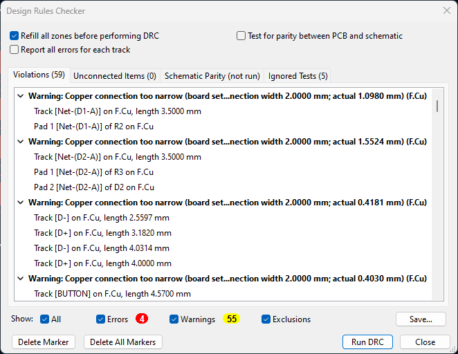
this is the not so embarrasing version of the error checker I had, since the first time I got arround 144 errors
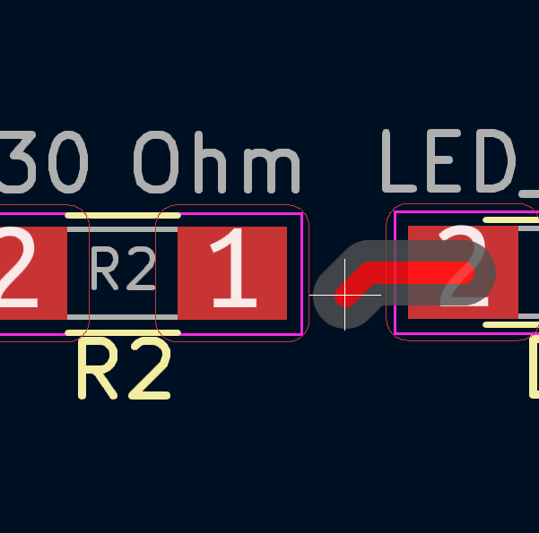
 One of the last (and hardest to solve) errors I had was the track crossing in diagonal, in the interior of a regulator through the clearance area.
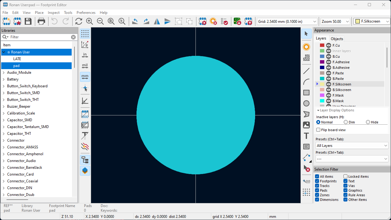
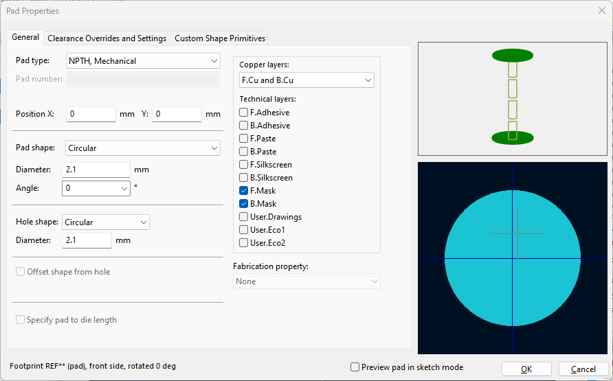
Since I was interested in screwing the board to some kind of envelope or board, I found you could modify a drill pad for this to happen. So I followed the steps of the previously recommended tutorial, and in the footprint editor I generated my own library folder, and modified this circular pads.
Finally for placing the logo goto File/Exporting/Graphics, search for the svg you have ready and adjust the scale after you have measured your free space left. Take in account the minimum width set for tracks, in my case .4mm.
Double click on the logo for the control points to turn on and right click, select create from selection / Create zone from selection, then the Create Copper zone from selection menu will appear, without any further changes I clicked enter and there, I had a copper zone for my logo.
I finished debbuging the tracks, by changing the orientation and place of connections, avoiding clearances, incrementing widths (you can do this for all of them at once in PCB Editor by selecting Edit / Set Track and Via Properties, filter items by net class or by layer, set the action to change the track width to a new preselected track width and then clicking ok) and ready! I passed my design rule checker.
I almost forgot, place the starting point (by clicking ‘S’) in the lower left corner.
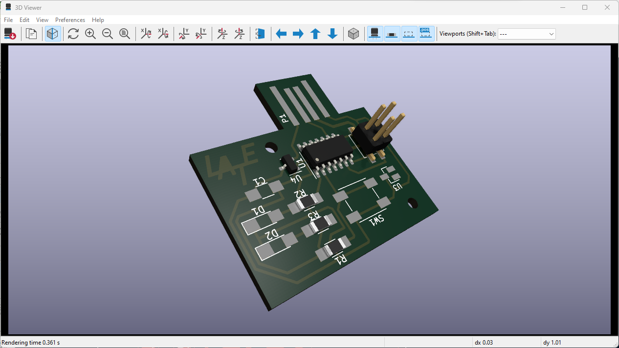
I really liked how this came out in the 3D Viewer (you may access it by pressing alt + 3) and raytracing the board
TIPS and TRICKS (not taken in account for this exercise): If you find yourself not being able to untangle the tracks (wiring in a plane) you may use vias (wiring connector from one side to another) to switch to the other side/plane of the board.
If you want still to keep it in one side but still haven’t found a way on how not to cross tracks (I personaly believe, there is always a way (at least so far)) yo may bridge over tracks by using a 0 Ohm transistor (remember this is a desperate measure, I didn’t have to use)
Export and Post-processing
In order to export the file for milling, go to file, export, SVG, and export the layers for milling in one export, and the layers for cutting in another export.


Open Mods and follow this steps:
- Right click on canvas
- Choose programs
- Open server program
- Under Machines, pick the one available in your lab, in my case is the MDX20
- Load each svg exported from KiCAD and calculate
*In the case of the milling, invert the image
You can download my KiCAD files from here:
- EDA RB.kicad_pcb
- EDA RB.kicad_pro
- EDA RB.kicad_sch