Week 9

Output devices

By Patricia Samudio Salinas β€” on

Ouptut devices

Hi there! πŸ‘‹πŸΌ Here I am... week 9 (weeks are going too fast 😨).

Well, after last week where several electronic boards were produced πŸ˜…, we've reached the week where we must establish communication between a controller and an output device 😯 To do this, the general documentation for the week is the first activity.

After choosing the output device (LCD Display), I review other materials to better understand the device. For that, this video was useful to me.

Additionally, I used the Wokwi simulator to experiment with connections, programming, and operation of an LCD Display + Arduino UNO πŸ™ŒπŸΌ.

Then, I start making the circuit πŸ˜… (adding hours of PCB production 😬). I choose the circuit included in the resources for the week: hello.LCD.44

Additionally, I supported work on these resources:


Patuino: PCB production

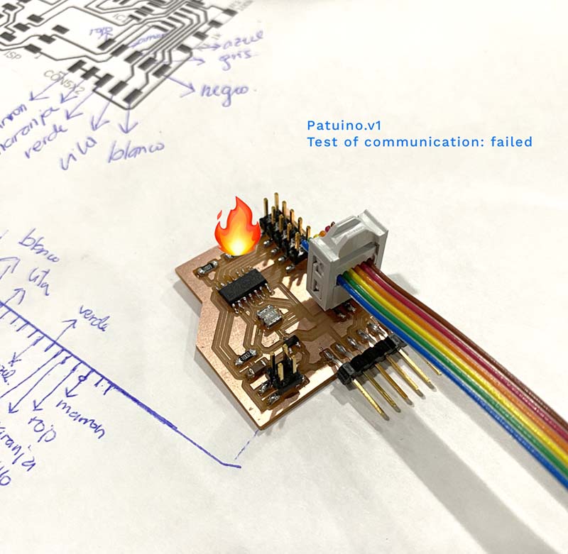
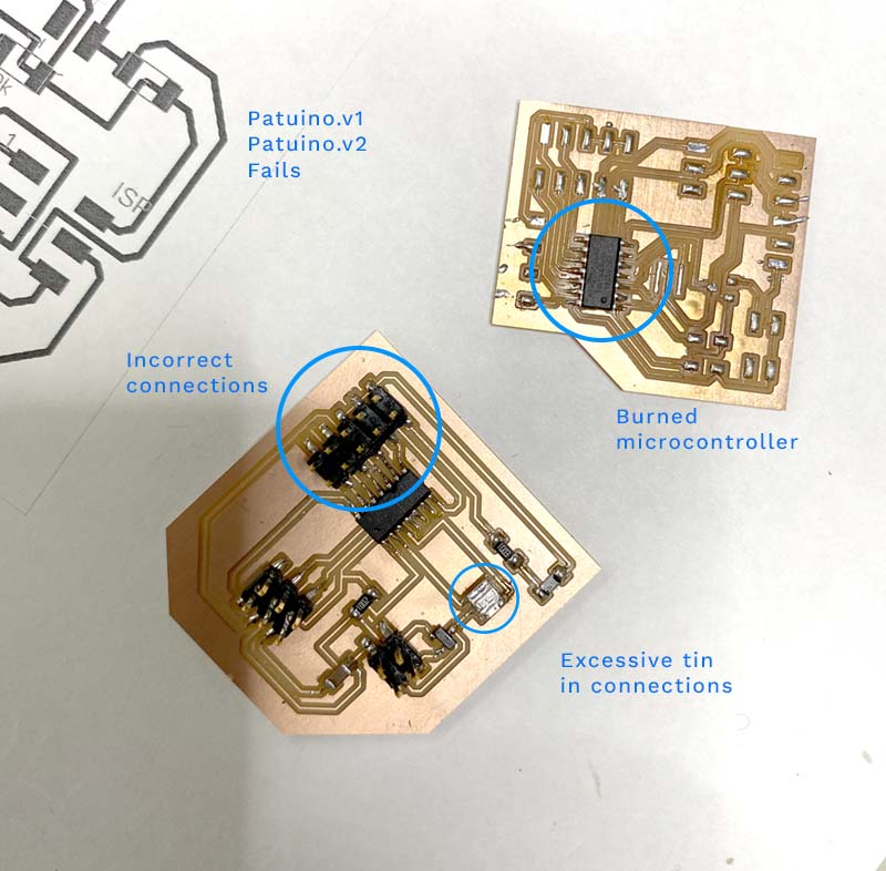
I must say that the production took me more than 2 weeks: the first board burned πŸ”₯ during a functionality test 🫣. Then I made two more boards that didn't produce communication ☹️ due to errors in soldering and connections between components; however, this was an opportunity to continue practicing with the FabLab equipment and soldering technique 😎.

Next, I share images of this part of the process.

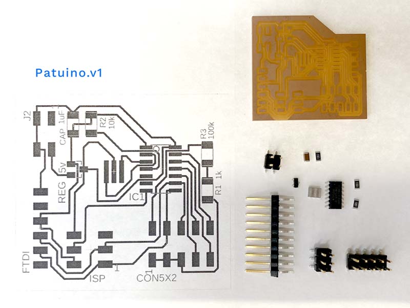
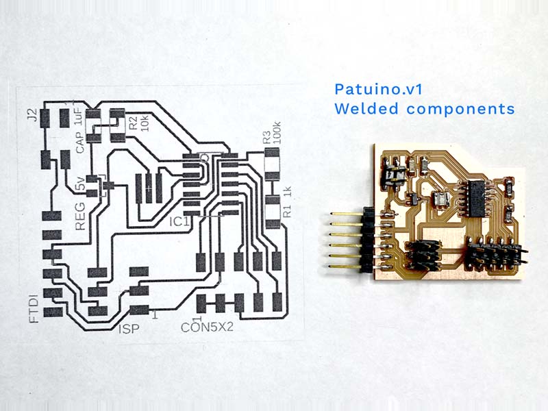
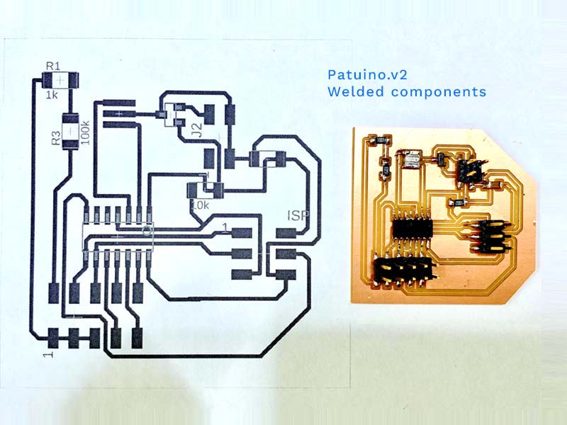
Patuino version 1: components, welding and fails.
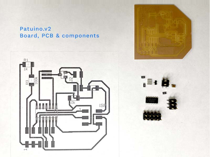
Patuino version 2: components, welding and fails.
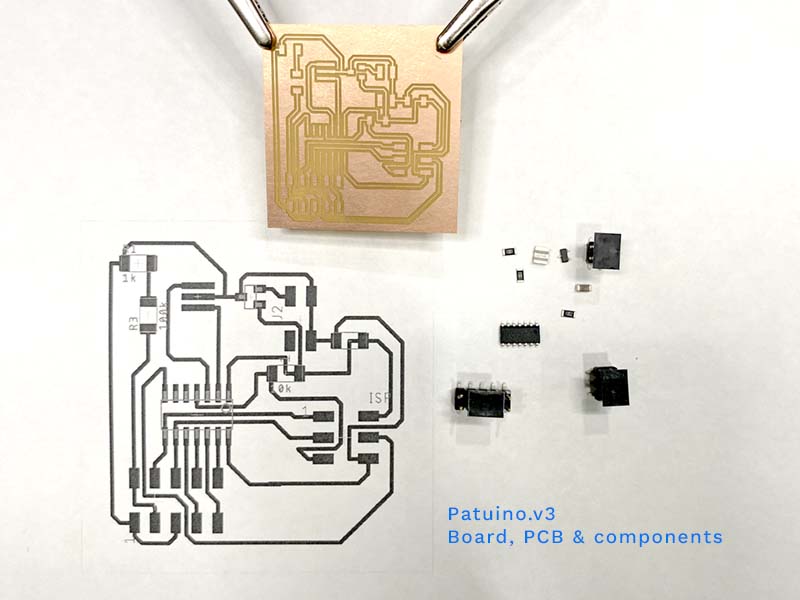
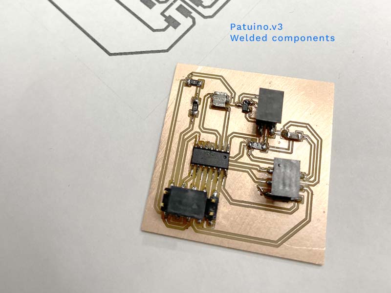
Patuino version 3: components, welding and fails.
πŸ“ From the burnt circuit board I learned: Verify the voltage of each component: if there is a component that operates at a higher voltage than the processor logic, attention should be paid to the connections between the voltage component and the regulator (when different voltage components are on the same PCB).
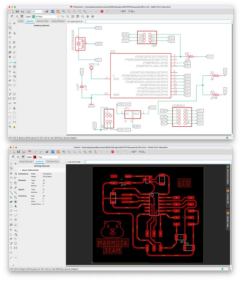
πŸ“ From all the non-functional boards, I learned: If the process involves generating the schematic from a board, it is good to first trace the schematic on paper to interpret the connections; then use EDA software for the schematic and design before moving on to the CAM process.

Patuino v4: the final

So, I went back. Together with Abdón, we checked the initial scheme and through that I was able to recognize several mistakes made: some connections were missing and others were wrong 😱. No problem! Let's start again: new scheme, new board 😎. But...

The almost final 🫠

Well, the end didn't turn out to be the end. 
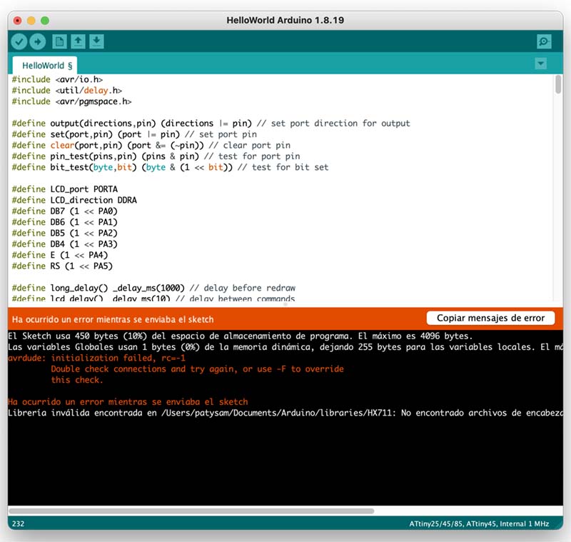
I ran a fifth plate: machined, ok - soldered, ok - initial test run, mmm, not so good. 
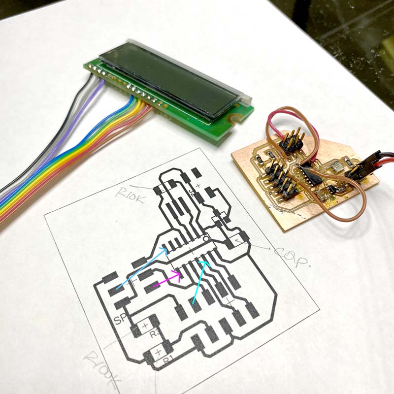
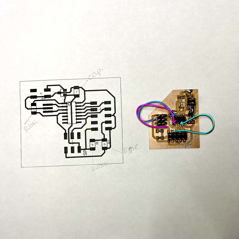
Reviewing board, schematic and layout again, the debugging process on the board begins: again, with guidance from Abdon, 'some physical adjustments' are made on the board. And the board was left with 'three suspension bridges', which finally gave a communication result! There remains the task of machining and soldering the last, last board.

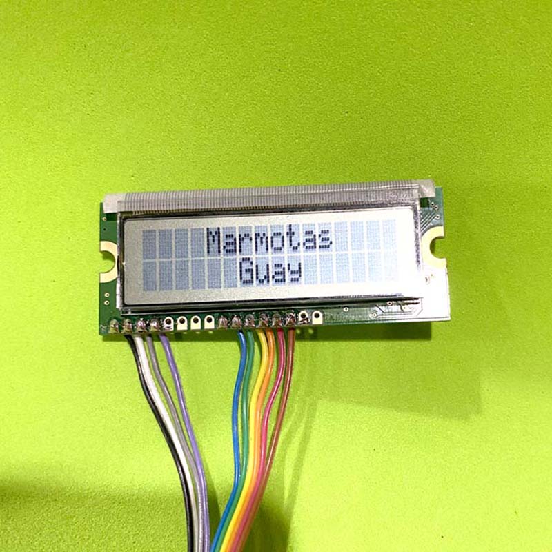
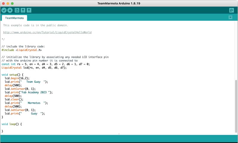
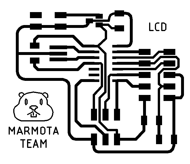
Patuino version 4: welding, debugging and LCD Display on.

Programming

The programming process was also quite long. At times, it was frustrating that there was no response. However, through this situation, errors in the connections were able to be detected and verified.

Errors in the transmision of the Code.

Anyway, let's see the route I followed to finally achieve the purpose. For programming, I used the Arduino IDE 1.8.19 because the programmer we have does not establish a connection with the latest version (2.1.0) when programming with some libraries, such as the one I had to use for the LCD Display. First, the parameters are determined from the Tools menu:

Tools > Board > ATtiny 24/44/84
Tools > Clock > External 16 MHz
Tools > Processor > ATtiny 44
Tools > Programmer > USBtinyISP


From the Sketch menu, I added the library: LiquidCrystal by Arduino, Adafruit. Then, I started a new project from the Example option > LiquidCrystal > Hello World. I defined the connection pins, loaded it, and verified the communication.


And so much for my learning path of designing, soldering and implementing a board to communicate information through an output device. 🀩


Marmota Team LCD Display Update

Over the next few weeks, I made adjustments to the PCB design, correcting the errors that occurred on the board that worked, and looks like this. It remains to machine it, solder the components and program it 😎.


What I learned

😎 Debugging an Electronic board.

😬 Verify, verify, verify the schema as many times as necessary.

How I learned it

By the assistant of the local instructors. πŸ™ŒπŸΌ

Making my product.

What I should do

πŸ™ŒπŸΌ Re-produce the plate with final adjustments.