Week 6 - Electronics design
Notes
- Voltage (V) - eagerness of electrons
- Current (I) - amount of electrons
- Ohm’s Law is that Power (P) - V*I
- Kirchhoff’s Current Law is that the Sum of voltage in a circuit is equal to the sum of all currents in a node is equal to zero.
- FET vs. transistor, when using an MC FETs are easier. Normal transistors are current-driven, and FETs are voltage-driven.
- GW Instek GDS-1152A Oscilloscope, setting the trigger, slope to the correct value.
- ATTiny 412, LED, button, switch, phototransistor.
- Remember to add a power connector.
- RX/TX pins need to be connected to a connector.
- UPDI 3 pin connector.
- Check out the reduced datasheet for 412.
- 4,5,7 are the pins that are free.
- Logic pin 6 connects to physical pin 2.
- Phototransistor should connect to something which has ADC (PA1, PA2, PA3).
- Trace +/- and tx/rx updi and ground.
- YT Digikey is a good learning resource.
- Place capacitor close to IC to protect from ripple on powerline.
- You can use a two-pin UPDI connection, but then you will have to power your board separately.
Individual assignment
redraw an echo hello-world board, add (at least) a button and LED (with current-limiting resistor) check the design rules, make it, and test that it can communicate
Design rules
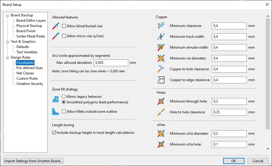
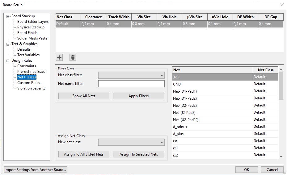
As we use a 0.4mm end bit to mill traces, and a 0.8mm end bit for the outline, it is important to define your design rules so as to leave a sufficient amount of space between the traces and pads. The outline is milled using a 0.8mm end bit and therefore there must be at least a 0.4mm distance from the outline to any traces or pads. In ‘board setup’ these values can be assigned to the design rules and net classes in KiCAD:
File > Board setup > Design rules > Constraints
File > Board setup > Design rules > Clearance
Once you have design you board you can then check if your design is in accordance with your design rules by go to the Design Rules Checker:
Inspect > Design Rules Checker
Designing the board
I started working in KiCad adding the components that I was sure of I would need, like the ATTiny412, VCC, Ground, and connectors. Then, I looked at some tutorials for electronics design basics, and decided I probably needed coupling and decoupling capacitors. I think I will need a ceramic capacitor near the IC. I am looking at this documentation trying to determine the capacitance of the capacitor. There are guidelines for signal frequency. Looking at this page on StackOverflow I chose to use a 1uF capacitor.
Based on the components on the SWD-D11C programmer, which have a 499 Ohm resistor before as well as after the LEDs, I decided to use the same resistance. Ok, rereading the assignment it turns out we are not making a board from scratch but rather adding some stuff to the hello world board. Also, I had imported the wrong fab library so I couldn’t find any of the components.
Now that I put some stuff on the board, the final question is what to do with the photoresistor. At least it has a relatively short datasheet. “Customer must apply resistors for protection, otherwise slight voltage shift will cause big current change (Burn out will happen).” Based on that line I decided to use a 10K resistor as well as other years using that resistance. However, the components were not quite the same so it might be incorrect.
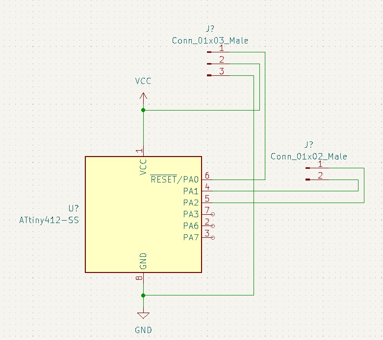
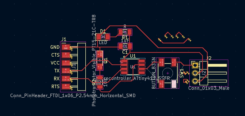
I started by adding the obvious connectors to the pre-defined pins on the board. I decided to use a three-pin UPDI connector so that I wouldn’t have to power the board externally when programming it.
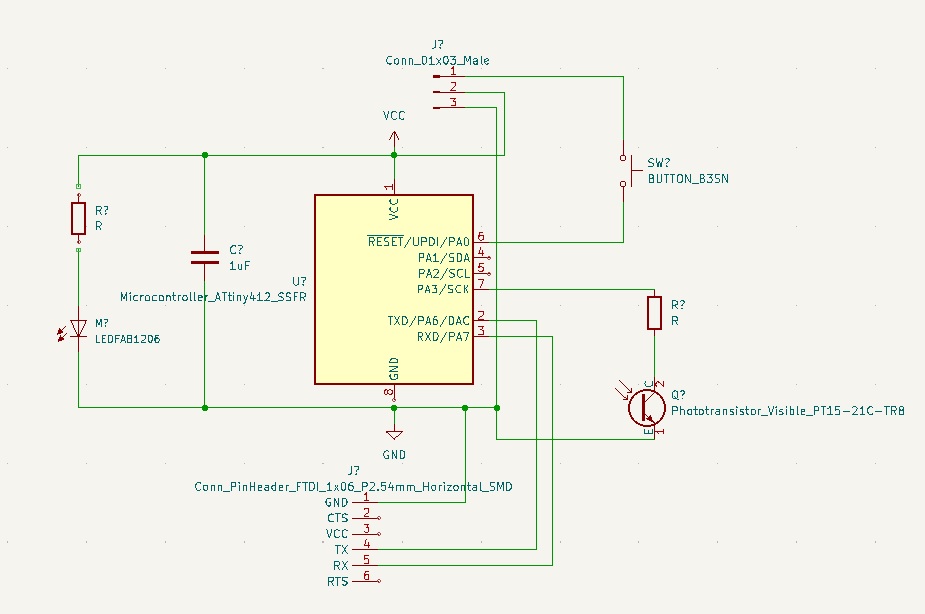
I added a 1uF capacitor as a ‘bypass capacitor’ close to the IC for stability. I also added resistors in front of the LED and photoresistor so that there would not be too much current going through them.
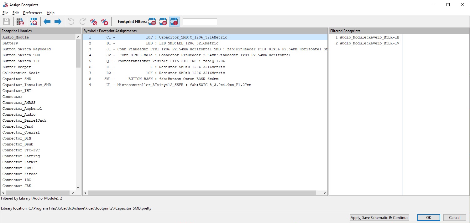
The next step was to assign footprints to components of which the footprint was unknown. For the resistors, I knew from previous assignments that we used the 1206 footprint in the lab, and that the LEDs were the same size as well. Following this, I went on to trace the connections between the components.
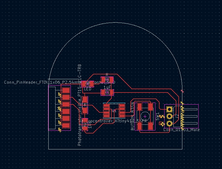
I followed this tutorial to create the rounded edges. I noticed during exporting that the size of the export was often bigger than the actual board. It turned out that the texts from the F.Fab layer were being included in the board width. I solved it by moving the text to with in the board outline, but I think there is probably a better solution.
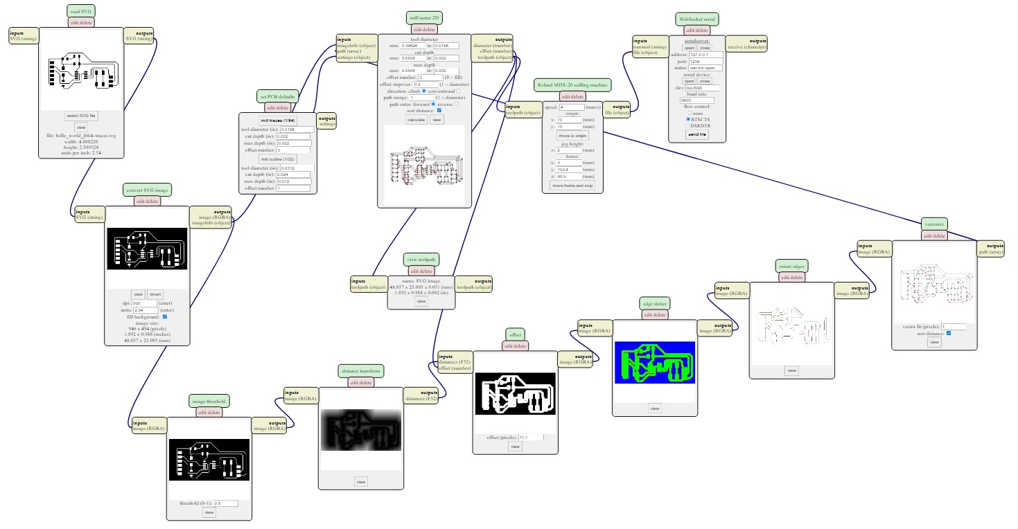
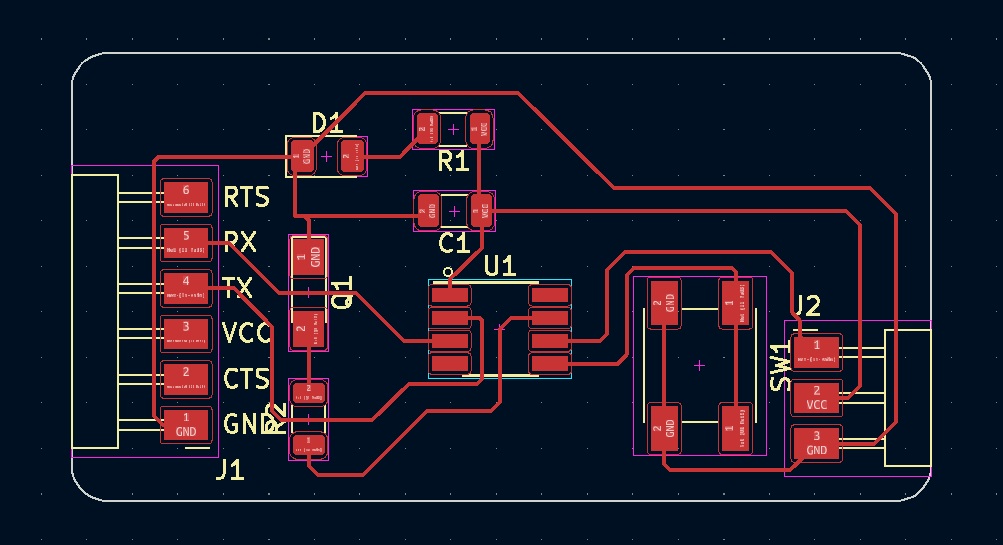
So, finally, a week later I was able to get my design checked by Henk. I had made a number of mistakes. In the schematic I had attached the Rx of the IC to the Rx of the FTDI, and the Tx of the IC to the Tx of the FTDI. Apperantly, this is wrong so I had to switch them around. Also, I had to connect the VCC of the FTDI to the VCC of the UPDI so that they can both power the board. In the PCB design I had not applied the design rules, so I had to redraw all the traces as well as correct the mistakes from the schematic. The resulting board (and its issues) are discussed in week 8.
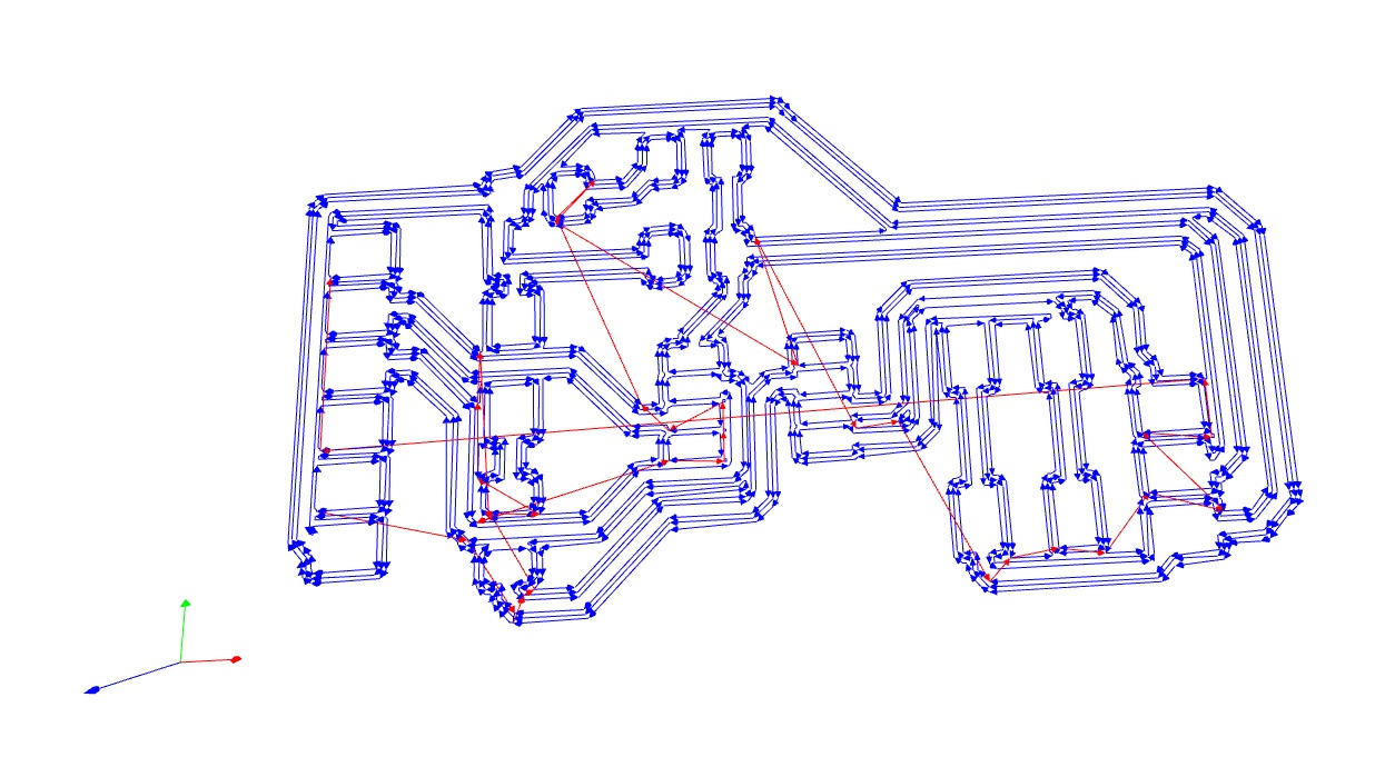
Here is a link to the compressed KiCAD project for the board that I designed this week, as well as the SVG for the traces and the SVG for the outline.