Electronics production
1. Group Assignment
A- Characterize the design rules for your in-house PCB production process: document feeds, speeds, plunge rate, depth of cut (traces and outline) and tooling.
B- Document your work (in a group or individually).
C- Document your work to the group work page and reflect on your individual page what you learned.
1.1. PCB Desktop Milling Machine
The Roland SRM-20 is the typical PCB milling machine in most fablabs. It's a desktop milling machine that will be used to manufacture PCBs as well as molds.
1.2. File Download
1.3. Mods
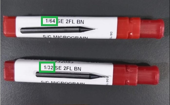
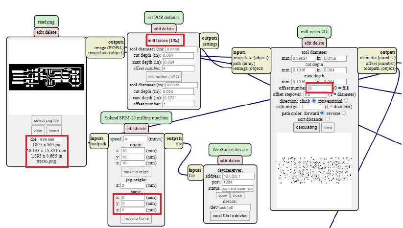
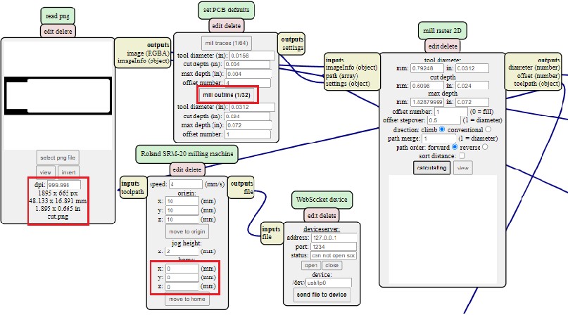
Mod was used to create rml files from png images. The rml extension is the accepted format for the Roland machine. The job is divided into two sections: the first is the machining of traces. We use the traces.png file and a 1/64" (0.4 mm) milling bit . the Second section is cutting outline. We use outline png file and a 1/32" (0.8 mm) milling bit.
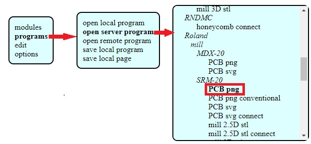
step 1: Open Mod
and Right click any whare. select programs - open server program - PCB png from Roland SRM-20 list.
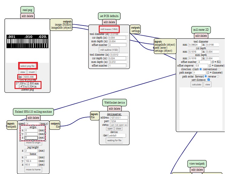
Step 2: On the “read png” block Click on select png file and choose the linetest.png
Step 3: Select mill trace from “set PCB defaults” block.
Step 4: On the “Roland SRM-20 milling machine” block let the origin coordinates 0,0,0
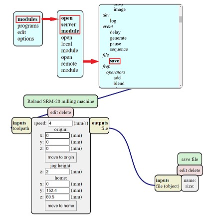
Step 5: Right click and select modules - open server module- save.
Step 6:- replace "websocte device" block with "save file" block .
Step 7:- Click on calculate in mill raster 2D block , The RML file will be downloaded automatically.
Note : you can have better finish if you make the offset more than 4 like 6 but it will take more time.
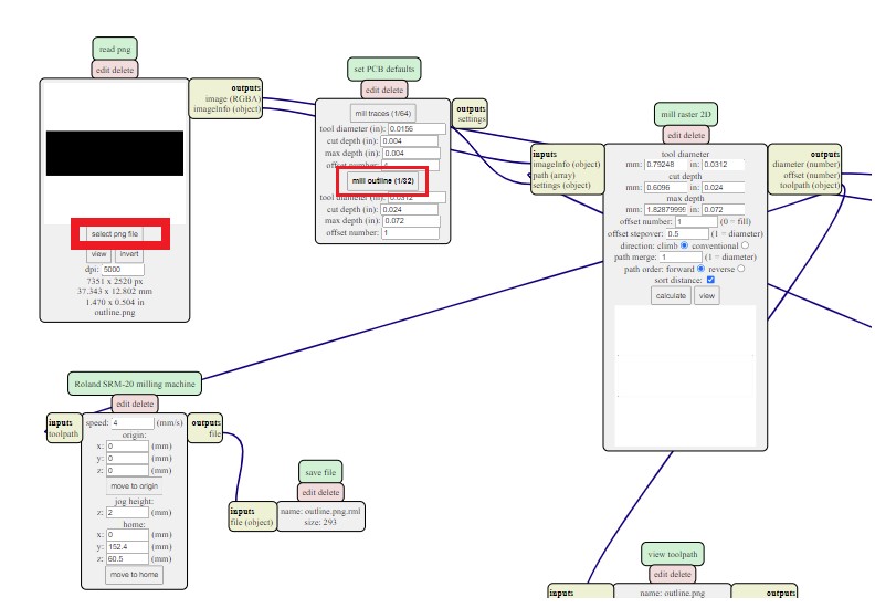
Step 8:Repeat the previous steps on the outline.png file, but click on the mill outline rather than mill traces from set PCB defaults block , to have outline.png.rml file
Note: check the job dimention to be 37.34*12.802 before calculate.
1.4. Milling & VPanel for SRM-20 software
Milling Bits
We used two milling bits; for traces 1/64” (0.4 mm), and for interiors 1/32” bit (0.8 mm).
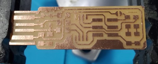
The circuit board (PCB)
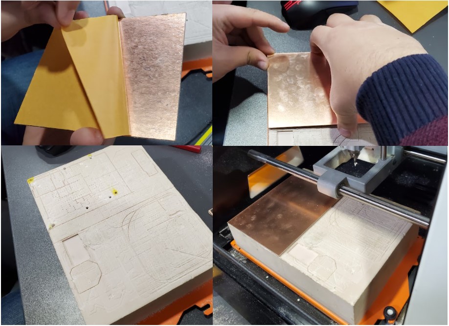
We used a FR4 single layer PCB (1.2 mm laminate thickness, 0.1 mm copper base thickness). Cut a piece slightly larger than the size of your design with a utility knife. At first, remove the bed, then put a double-faced tape on the board Remove the lower paper of the double-faced tape then fix it on the bed after that Install the bed.
Note, make sure that the face of the bed is smooth and there are no bubbles between the adhesive and the pieces.
VPanel for SRM-20 software (PCB)
Now we can mill and cut the board design using the rml files. first of all we must identify the mill bit's origin.
Step 1: Open the VPanel program and go to the dropdown menu and pick "Machine Coordinate System."
Step 2: move the head over the bottom left corner of the PCB, use the arrows in red box. then raise the head , use the "+Z" arrow to create enough space between the spindle and the PCB.
Step 3: Install the 1/64" milling bit in the spindle collet, keeping roughly 25% of its length outside.
Step 4: Using the "-Z" arrow, lower the spindle until the distance between the PCB and milling bit tip are about 5 mm . Untie the fastening screw while holding the milling bit between your fingers. Lower the milling bit until it makes contact with the PCB. Tighten the fastening screw.
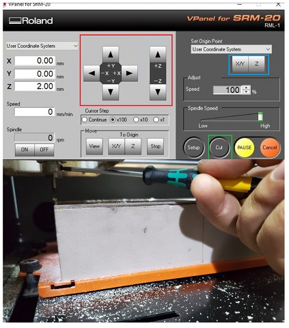
Step 5: Select "User Coordinate System" from the "Set Origin Point" by clicking on "XY" and "Z" in blue box . In the user coordinate system, this will make the current position the home or zero position.
Step 6: Move the milling bit a few millimeters above the PCB.
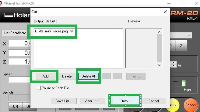
Step 7: Select "Cut" and then "Delete All" to get rid of any outdated jobs. Select the traces rml file by clicking "Add." finally Choose "Output" Now is the time for the machine to start.
Step 8: When the first job is finished, go to the "Move" menu and select "XY". The spindle will be moved to the "XY" home . lift up milling bit , cover it and remove it. after that install milling bit 1/32".
Step 9: Repeat steps 4 to 7 with "outline.png .rml"file, but don't change x , y coordinate for origin "home coordinate".
1.5 Hero Shoot !
2. Individual Assignment
Make an in-circuit programmer that includes a microcontroller by milling and stuffing the PCB, test it to verify that it works.
2.1. Introduction
The PCB we'll be milling is known as FabISP, which stands for In-System Programmer. This programmer is for Atmel's AVR Microcontrollers, which are a family of microcontrollers. .The Roland SRM-20 is the typical PCB milling machine in most fablabs. It's a desktop milling machine that will be used to manufacture PCBs as well as molds. The design of a PCB is the first stage, but this week we already had the pre-designed FabISP, so we went straight to milling.
2.2. File Download
2.3. Mods
Mod was used to create rml files from png images. The rml extension is the accepted format for the Roland machine. The job is divided into two sections: the first is the machining of traces. We use the traces.png file and a 1/64" (0.4 mm) milling bit . the Second section is cutting outline. We use outline png file and a 1/32" (0.8 mm) milling bit.
step 1: Open Mod
and Right click any whare. select programs - open server program - PCB png from Roland SRM-20 list.
Step 2: On the "read png" block Click on select png file and choose the traces.png file
Step 3: "Select mill" trace from "set PCB defaults" block.
Step 4: On the "Roland SRM-20 milling machine" block let the origin coordinates 0,0,0
Step 5: Right click and select modules - open server module- save.
Step 6:- replace "websocte device" block with "save file" block .
Step 7:- Click on calculate in mill raster 2D block , The RML file will be downloaded automatically.
Note : you can have better finish if you make the offset more than 4 like 6 but it will take more time.
Step 8:Repeat the previous steps on the "cut.png" file, but click on the mill outline rather than mill traces from set PCB defaults block , to have cut.png.rml file
Note: check the job dimention to be 37.34*12.802 before calculate.
2.4. PCB Fabrication
Milling Bits
We used two milling bits; for traces 1/64” (0.4 mm), and for interiors 1/32” bit (0.8 mm).
The circuit board (PCB)
We used a FR4 single layer PCB (1.2 mm laminate thickness, 0.1 mm copper base thickness). Cut a piece slightly larger than the size of your design with a utility knife. At first, remove the bed, then put a double-faced tape on the board Remove the lower paper of the double-faced tape then fix it on the bed after that Install the bed.
Note, make sure that the face of the bed is smooth and there are no bubbles between the adhesive and the pieces.
VPanel for SRM-20 software (PCB)
Now we can mill and cut the board design using the rml files. first of all we must identify the mill bit's origin.
Step 1: Open the VPanel program and go to the dropdown menu and pick "Machine Coordinate System."
Step 2: move the head over the bottom left corner of the PCB, use the arrows in red box. then raise the head , use the "+Z" arrow to create enough space between the spindle and the PCB.
Step 3: Install the 1/64" milling bit in the spindle collet, keeping roughly 25% of its length outside.
Step 4: Using the "-Z" arrow, lower the spindle until the distance between the PCB and milling bit tip are about 5 mm . Untie the fastening screw while holding the milling bit between your fingers. Lower the milling bit until it makes contact with the PCB. Tighten the fastening screw.
Step 5: Select "User Coordinate System" from the "Set Origin Point" by clicking on "XY" and "Z" in blue box . In the user coordinate system, this will make the current position the home or zero position.
Step 6: Move the milling bit a few millimeters above the PCB.
Step 7: Select "Cut" and then "Delete All" to get rid of any outdated jobs. Select the traces rml file by clicking "Add." finally Choose "Output" Now is the time for the machine to start.
Step 8: When the first job is finished, go to the "Move" menu and select "XY". The spindle will be moved to the "XY" home . lift up milling bit , cover it and remove it. after that install milling bit 1/32".
Step 9: Repeat steps 4 to 7 with "cut.png .rml" file, but don't change x , y coordinate for origin "home coordinate "
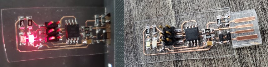
Rsults
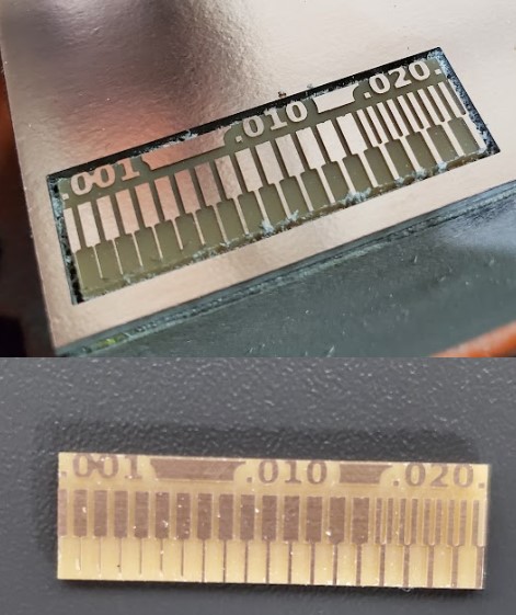
Flexible PCB
1- insert the image to cut studio
2-right click on the image and select Image outline
3- click on extract contour line
4-delete the image and move the outline to origin
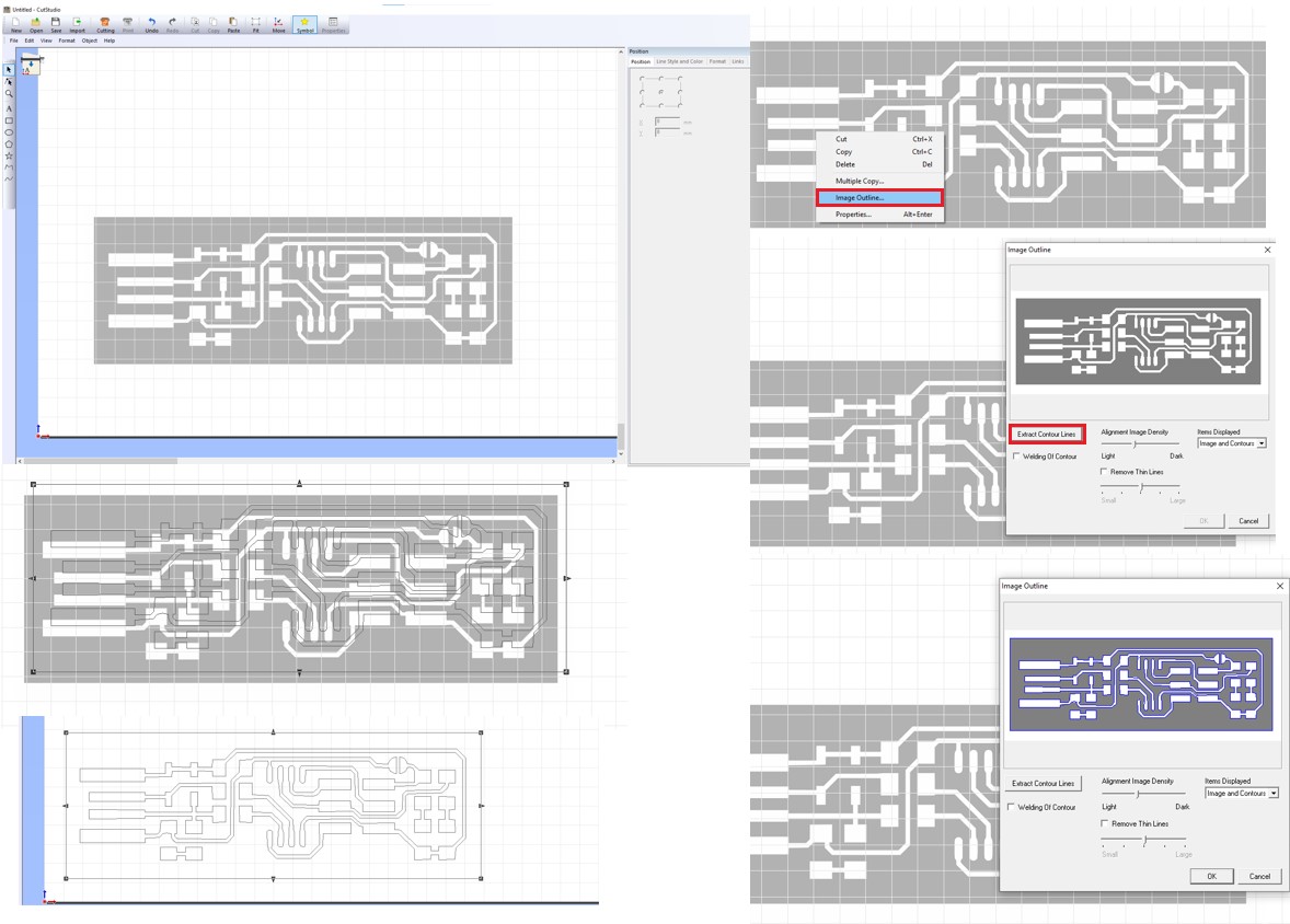
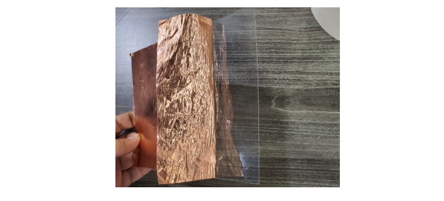
5-Cut the piece of PVC and put the copper sheet on it, make sure that there are no bubbles between the copper and the PVC sheet.
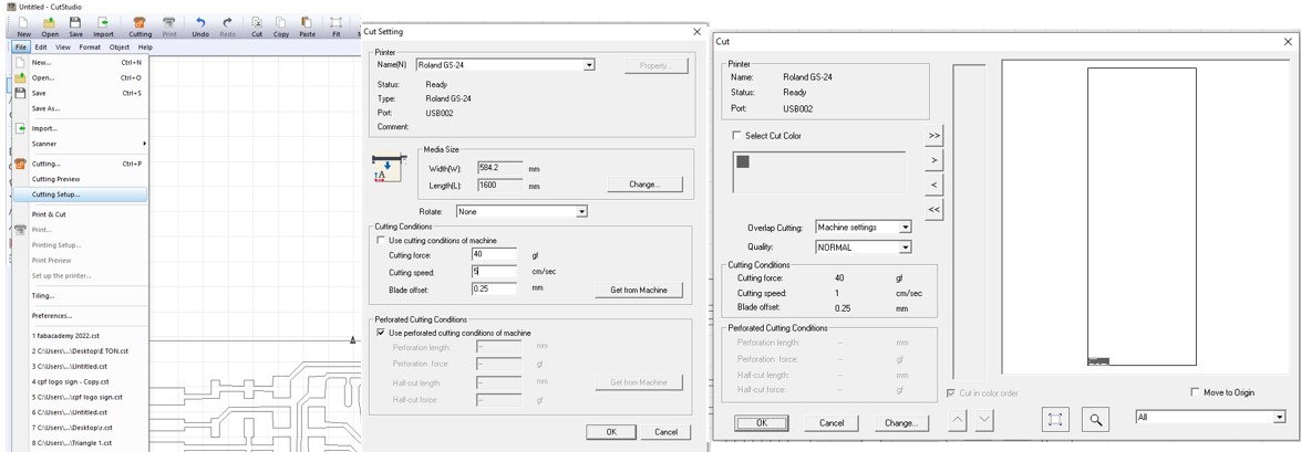
6- From file list select cutting setup.
7- Change the speed and force to 5 and 40 then click ok.
8- Press "control +p".
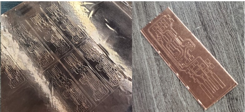
Rsults
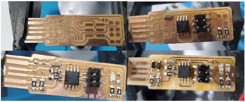
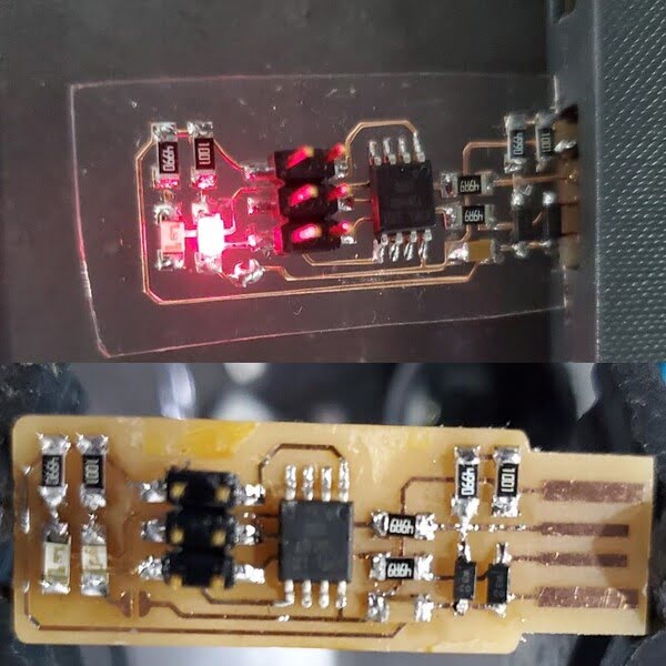
2.5. Assembling the PCB
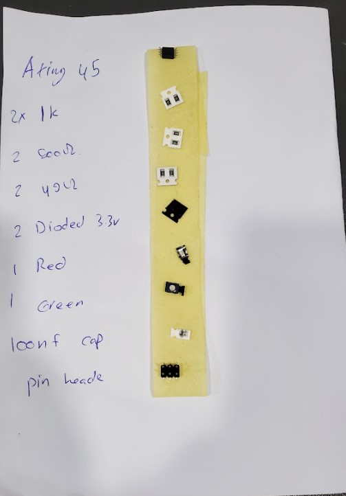
Obtain the components:
1x ATtiny45 or ATtiny85
2x 1kΩ resistors
2x 499Ω resistors
2x 49Ω resistors
2x 3.3v zener diodes
1x red LED
1x green LED
1x 100nF capacitor
1x 2x3 pin header
The LEDs and resistors are optional; the red LED illuminated when the target circuit is turned on, and the green LED illuminated when the programmer communicates with the target.
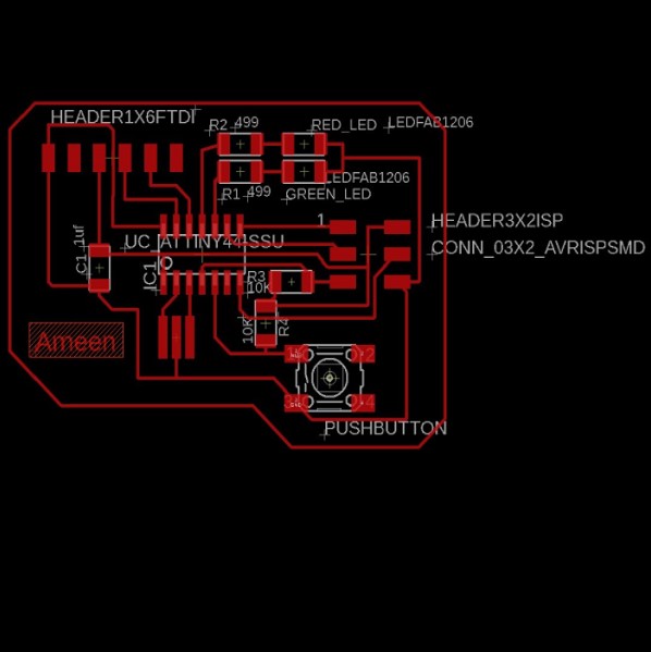
Use the schematic and board image below as a reference for component values and placement while soldering the parts to the PCB.
- Note the components that must be installed in the correct orientation:
- -The zener diodes are marked, both in the drawing and on the packages, with a line on the cathode side.
- -The LED cathodes on the PCB drawing are marked with dots and thicker lines. If you do not find the dots and thicker lines , determine the cathode using a multimeter.
- -The ATtiny45 marks pin 1 with a dot laser-etched into the corner of the package. Pin 1 is marked in the drawing with a dot as well.
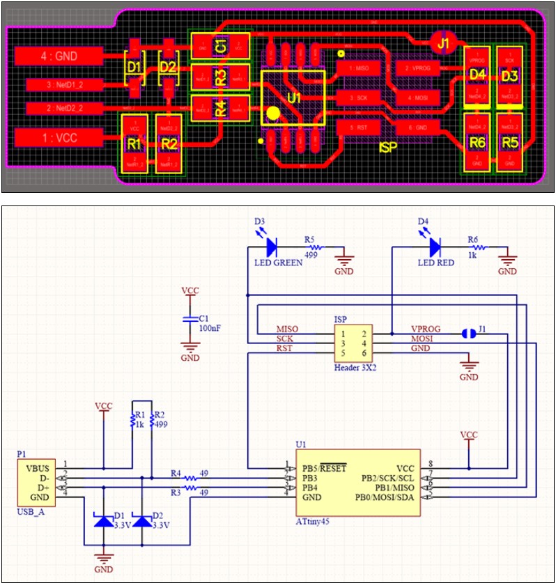
Use solder to create a bridge on the jumper.
Rsults
2.6. Check Your Work
It is always a good idea to double-check your work before connecting a board. It simply takes a few minutes and might save you a lot of trouble in the future.
Verify that you have inserted the necessary components in the correct places and orientations by comparing your board to the schematic and PCB layout image.
Visually inspect your board. Components should be flat on the board with pins in the air, not slanted. Solder connections should be fluid, with solder flowing smoothly onto both the pin and the pad. You probably don't have a strong connection if there is still a lot of exposed copper on the pad or if the solder is lumpy and pulls up into a point where you withdrew the iron.
Use a multimeter to check for shorts between VCC and GND.
2.7. Programing
These steps are for Windows users. It will be divided into three parts 1-Software Installation 2-Build the Firmware 3-Program the ATtiny45
2.7.1 Software Installation
Install Git
It's easy to install, and if you're using Git on Windows, you might have it already. Click the Start menu and search for "Git Bash".If not, download and install
Git for Windows.
Install GNU Make
Download
GNU Make.
when you installet accept the default location "c:\Programe Files (x86)\GnuWin32
Install avrdude
Download
avrdude Uncompress the file, and put it inside C:\Program Files.
Visual Studio 2022
Download
Visual Studio 2022
Atmel studio 7.0 Download
Download
Atmel studio
avr8-gnu-toolchain-3.6.2.1778-win32.any.x86
Download
toolchain Uncompress the file, and put it inside C:\Program Files.
Add paths
When you type the names of the tools you've just installed on the command line, we need to inform Windows where to look for them. search about choose "Advanced System Settings" in start menu and click on it
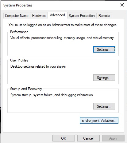
click the "Environment Variables" button Under User variables, select "Path" and click the Edit button.If you don't have a variable named "Path," create one by clicking the New button, entering "Path" without the name, then filling in the value as shown below.
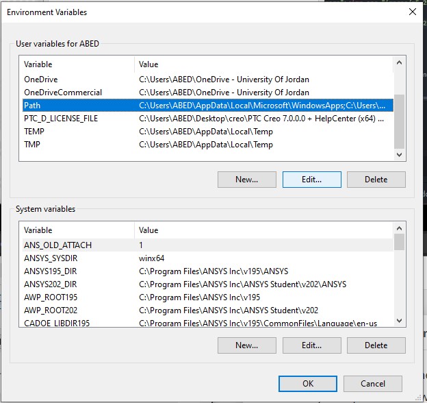
Add this three paths separately
C:\Program Files\avr8-gnu-toolchain-win32_x86\bin
C:\Program Files (x86)\GnuWin32\bin
C:\Program Files\avrdude
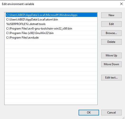
On all of the windows you've opened, click OK.
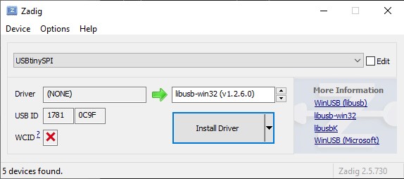
Install Drivers
If you using a FabISP, FabTinyStarISP, or another USBtiny-based programmer you mut do this step. If you're using one of the official Atmel programmers instead, use Atmel Studio is the quickest way to receive the drivers.
Download
Zadig and launch it.Connect your programmer and choose "USBtinySPI" from the list of devices. (If it doesn't appear, go to the Options menu and select "List All Devices"). libusb-win32 or libusb0 are the drivers you want to install (to the right of the green arrow). Select "Install Driver"
Sanity Check
Everything is now up and running. Let's make sure everything is in working order. open Git Bash "The terminal window you should use"
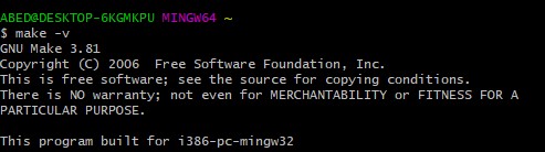
Check make
Enter the command "make -v". You should check out:
If you get a "command not found" error, double-check that you installed it correctly and that your path variable settings are accurate.
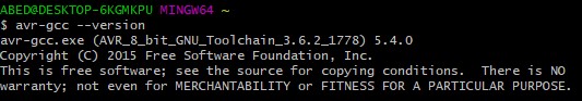
Check avr-gcc
Enter the command "avr-gcc --version". You should check out:
If you get a "command not found" error, double-check that you installed it correctly and that your path variable settings are accurate.
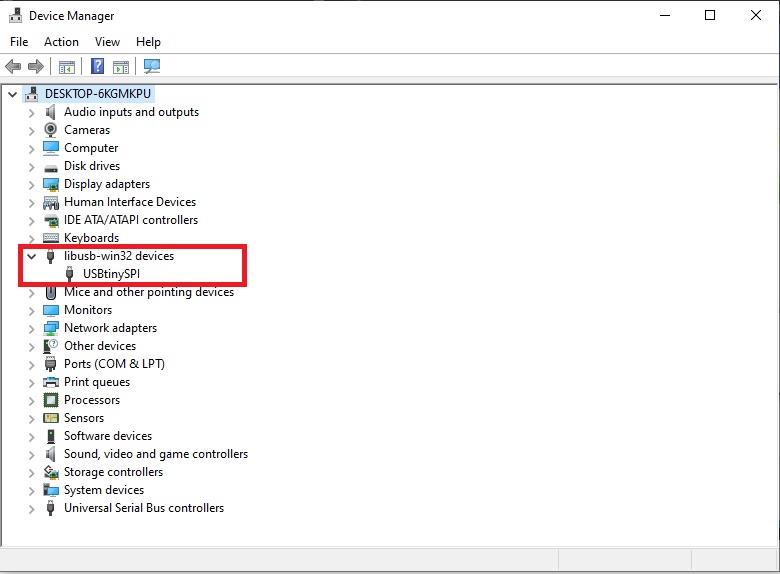
Check that the programmer is listed it “Device Manager”
Check avrdude
Enter the command "-c usbtiny -p t45". You should check out:
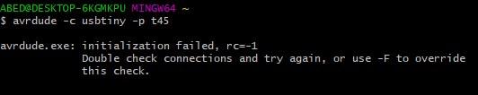
This indicates that avrdude discovered your programmer but was unable to communicate with a target board (which is to be anticipated given that we don't have anything connected to the programmer at the moment).
If you see:
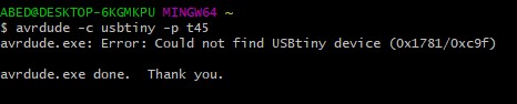
Check your USB driver installation (the Zadig steps).
If you get a "command not found" error, double-check that you installed it correctly and that your path variable settings are accurate.
2.7.2. Build the Firmware
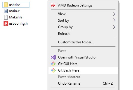
Extract the firmware source code from the zip file and Git Bash in the folder.
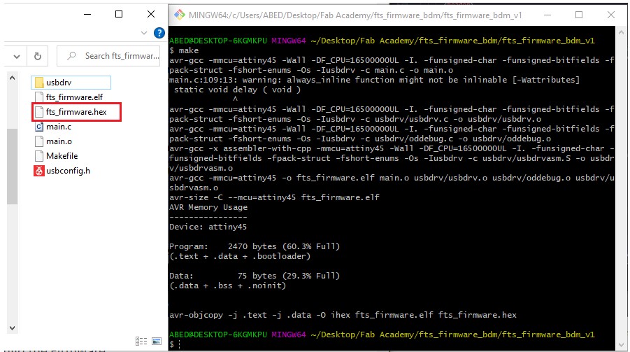
Type make, This will generate the hex file for programming the ATtiny45. If the command fails, something is amiss with your toolchain installation.
2.7.3.Program the ATtiny45
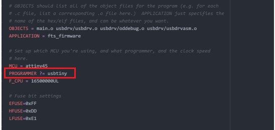
First, open "Makefile" in any text editor from the file where you extracted firmware source code.
Near the top of the file, look for the line that say :PROGRAMMER ?= usbtiny Replace usbtiny with the cod of the program you're using and save it.
- Small translucent blue programmer: avrisp2
- Large translucent blue programmer: jtag2isp
- White box with blue stripe: White box with blue stripe: atmelice_isp
-Any fabbed board with an ATtiny on it: usbtiny
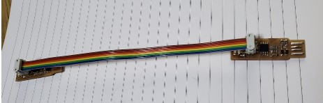
Connect the programmer's header to the FabTiny ISP target board's header. check the connection between programmer and FabTiny ISP pin 1 to pin 1 , and so on. Connect the programmer to the USB port on the PC. Both boards should have red LEDs that light up.
Not:It's also a good idea to use a USB extension cable This reduces the damage if there is a problem
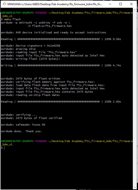
Run "make flash" in the "Git Bash" command window. The file "fts firmware.hex" will be programmed into the target board's flash memory with this command.
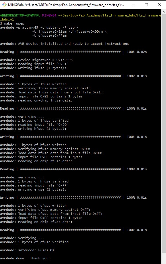
Run "make fuses" in the "Git Bash" command window. This command will program the FabTiny ISP target board's parameters to make it a programmer.
Disconnect both boards' cables, disconnect the programmer, and plug the FabTiny ISP into the USB port. If everything is working properly, the red LED should light up, and your board should be identified as "USBtinySPI" in Windows device management.
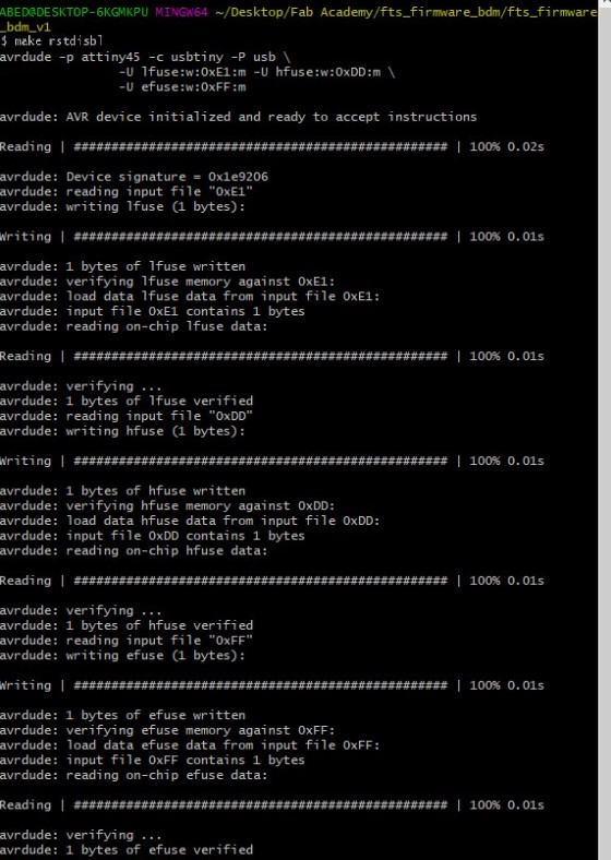
Connect the programmer, the FabTiny ISP, and the USB port again.Run "make rstdisbl" in the "Git Bash" command window. This command prevents the FabTiny ISP from being reprogrammed in the future.
Now You should now have a fully functional ISP programmer!
2.8. Test the USB Functionality
Chack Windows lists USB devices in Device Manager (Start → Control Panel → System → Device Manager), USB devices can also be found in the "Devices and Printers" or "Hardware and Sound" categories.
Also you can try programming another board with your board.


