7. Electronics design
This week I worked on a redrawing a hello world board and familiarizing with the various testing tools available in the lab.
Overview
We learnt some common compoenents found on a microcontroller PCB. So of which are:
- Resistors -> V = I*R
- common figures/numbers -> 499Ohms, 4.99kOhms etc.
- we use 1206 form factor
- Capacitors -> C = Q/V
- polarized and non-polarized
- easy to charge
- Buttons
- Ribbon cables
- Diodes
- current goes to the direction of the “arrow”
- 2 terminals, anode and cathode
- voltage drop
- leakage
- sharp drop -> zener diode
- use less due to better integrated processors
- LEDs: green line is the cathode side! only one side!
- color, max current
- current limiting resistors
- view datasheet
- Crystals
- drawn like a capacitor, but with material in between. Converts mechanical to electrical energy, and has a peak to determine time
- Inductors -> U = L dI/dt
- transistors
- MOSFETs: R(ds) -> resistance between drain and supply. Typically in the milliohms range
- Regulators: ensures a steady output current. Accompany with capacitors!
- Op-Amps: difference between 2 voltages, and amplifies the signals. These are now usually built into the current system
- microcontrollers:
- We will use UPDI based ones: ATtiny412, ATtiny1614, etc.
- To explore in future: SAMD chips
Next, electronics design and how to draw circuits
- Kirchoff’s law: all nodes into a node add up to 0.
- P = I^2 _ R = I _ V
- EDA: electronics design automation. For EDA tools, look at Eagle, KiCad, etc.
- use libraries that contain components
- place components, then draw route
- statisfy design rules
- TinkerCAD: very convinient for simulating
- Rats Nest
- draw routes, draw outlines
- draw interior for mods to know where to cut
- mods treat while is high, black is low. Depends on image, we need to invert it.
- Get libraries:
- fab libraries
- SnapEDA
- Simualators and more!
To get started, we learnt how to use the testing tool to debug our circuit boards
Tasks
- Learn about testing tools
- Setup EDA tool
- Redraw Hello Board with minimally a button and a LED
- Solder Hello Board
- Test Hello Board
Group Assignment
TODO: link to group assignment page
This week was relatively straightforward. We have 3 main tools: Oscilloscope, Power Supply, Multimeter
- Oscilloscope: We can measure frequency, analog voltage levels between 2 points, scale, freeze the wave.
- Power Supply: This provides clean power, set current limit (note that is not the current running, but a limit!)
- Multimeter: Check voltage, capacitance, diode, resistance, and continuity to check for shorts.
Assignment
Setup
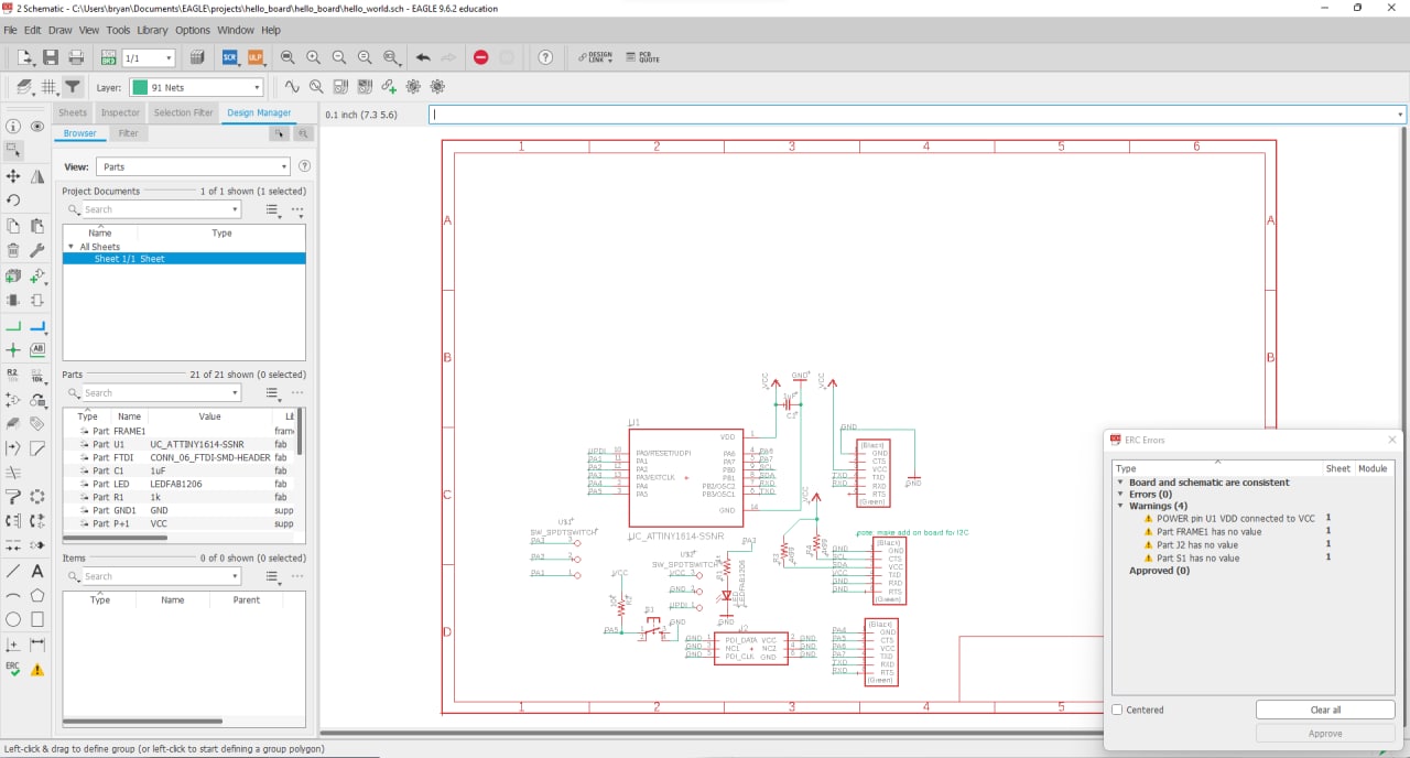
I setup Eagle by following this guide.
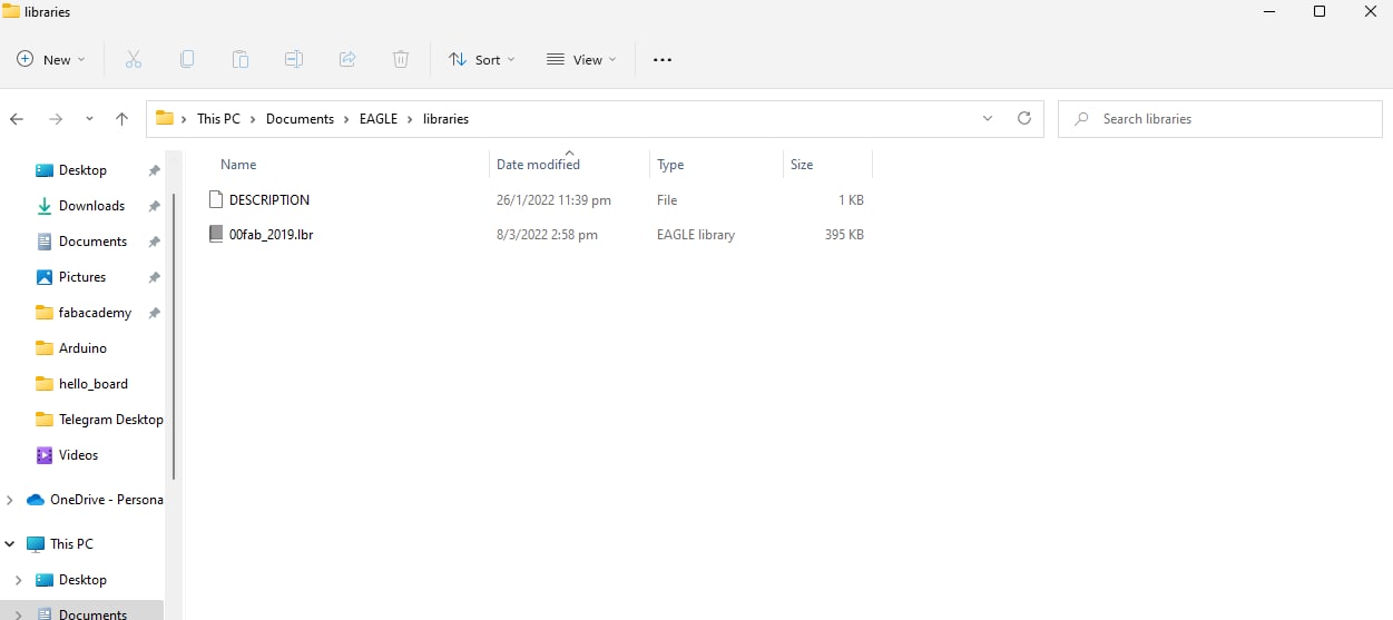
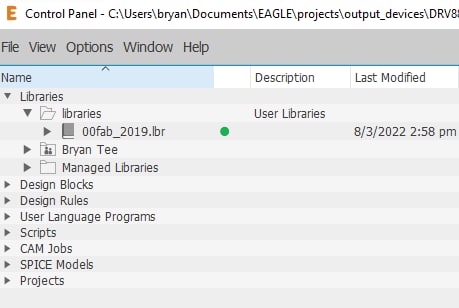
After installing Eagle, I downloaded fab.lbr
However, preview seems to not be working; verified that my Eagle installation is fine as I can view the previews of Eagle Pcb. Instructor Steven gave us the 2019 version of the library, and it seems to be functioning properly.
Ensure that fab is being used by right clicking the library and ensure there is a green dot beside it.
Redrawing the board
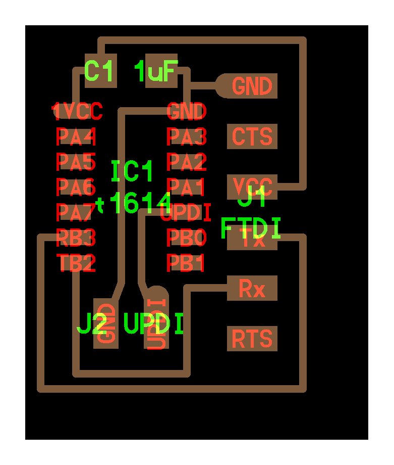
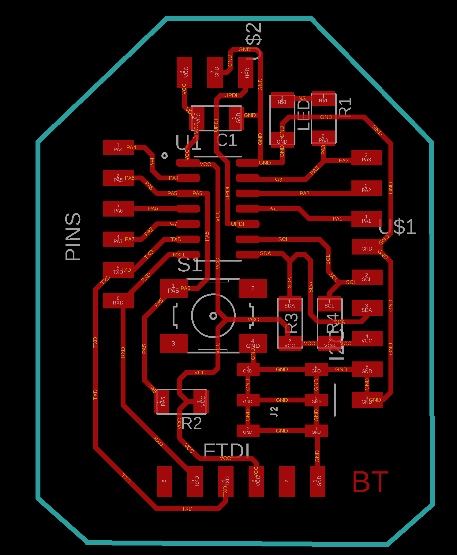
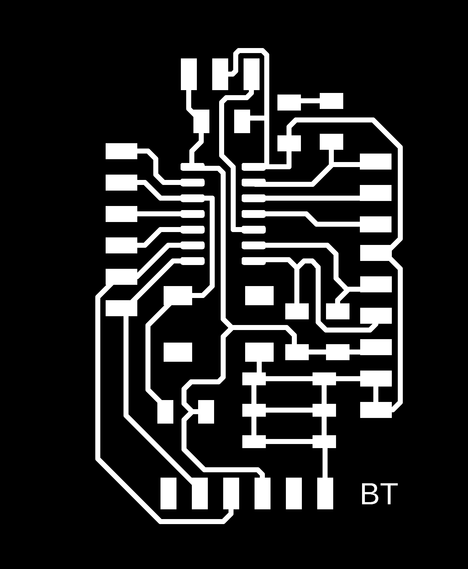
Although I am a beginner, I was curious how “complex” can ATtiny1614 be. Also, if I am familar with it, perhaps I will get a chance to use it in my final project? However irrational that thought process was, that was why I chose to redraw an ATtiny1614. I also decided to expose the I2C portion as well as all the pins available on the Tiny1614. The key components that ATtiny needed were a capacitor based on the hello world diagram . Next, I also took a look at Adrianino’s 1614 board.
First I created the schematic. Credits to Steven, as he showed us step by step how to use Eagle (although I was not able to absorb very well). The key things that I remembered were:
- Use 1206 components wherever possible
- Add a frame
- Add components
- Wire components with net
- Click SCH/BRD button
- Arrange for better Rats Nest
- Routing (manual/auto)
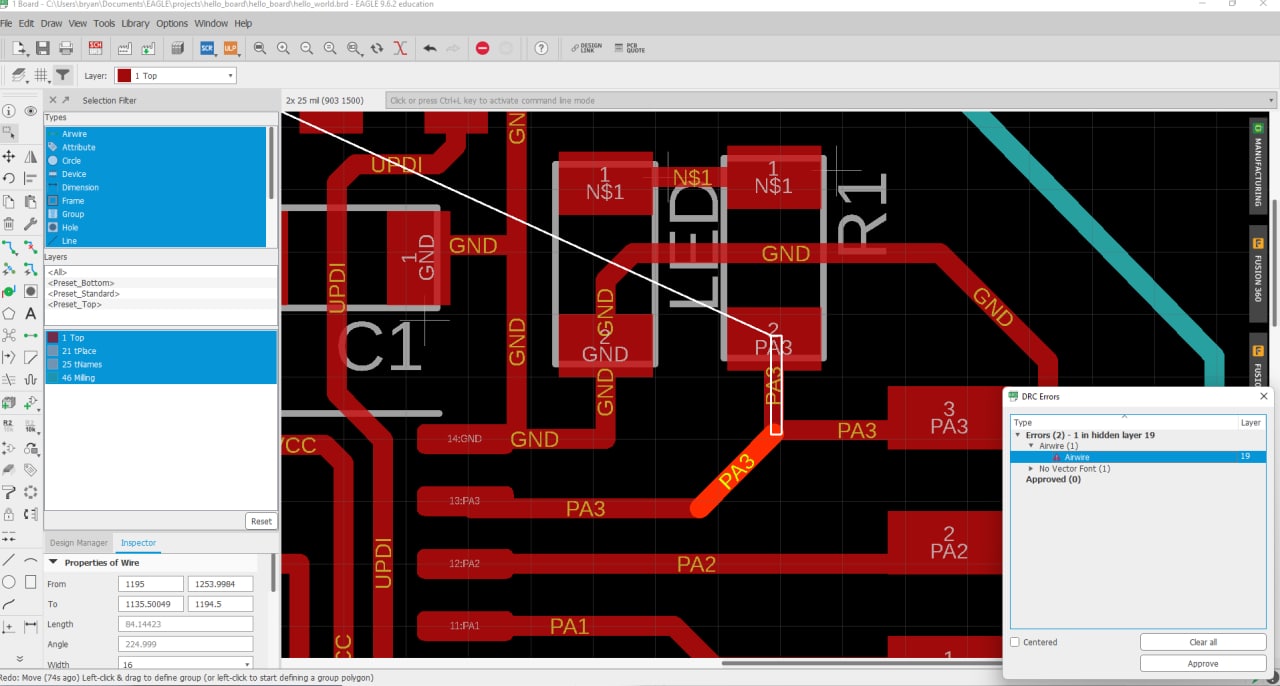
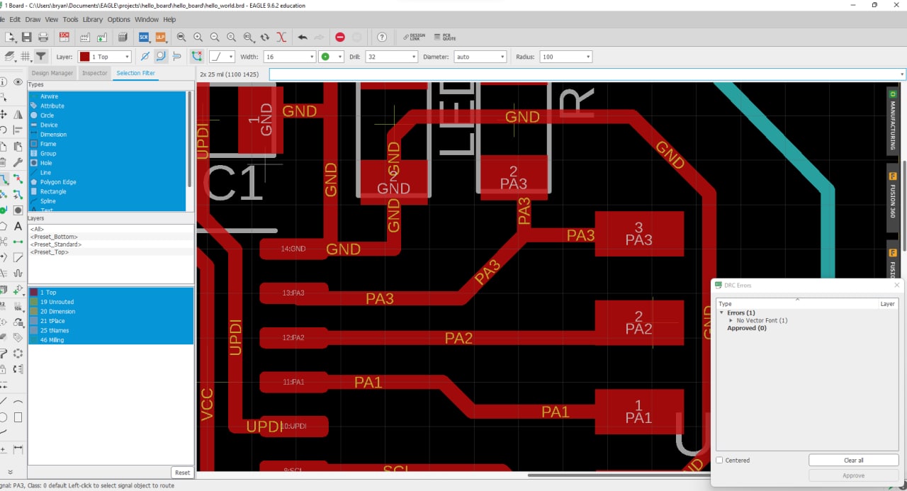
- Design Rule Check
- Draw Milling outline
- Export Top Layer and Milling layer separately
- specify monochrome and resolution 1000-2000
- Use mods to generate gCode and mill on StepCraft
These commands were the ones I found most commonly used:
add: adding a componentmove: move a componentdelete: delete a component/route/netlabel: Add label to components in schematicname: Add name to components in schematicroute: Route components between pathsnet: Connect components in schematicvalue: Add values to components such as resistors, capacitors, etc.
These are important icons that I used:
Grid: I frequently change between setting “50 1 5” and “25 2 1”. This helps with moving components to follow DRC and aligning parts .Layer: Change layer visibility to view onlyToporMillor enable alltopcomponents to arrange the components nicely
Combining all the above, I made the schematic as well as the final design
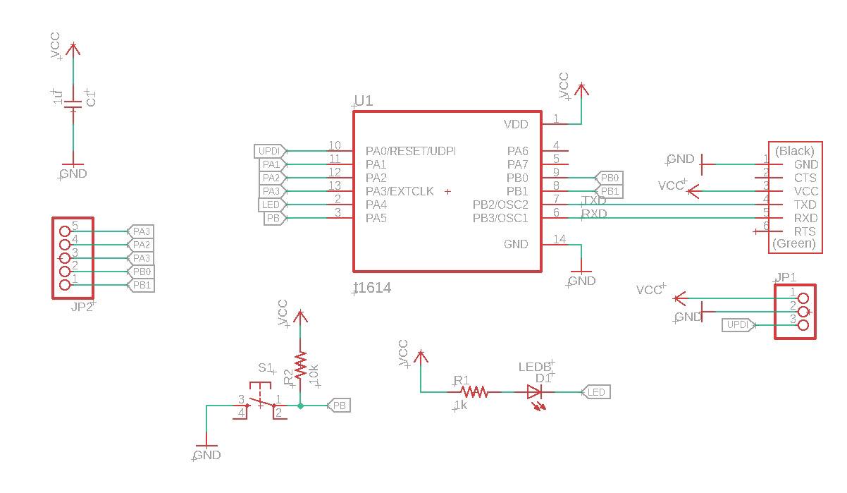
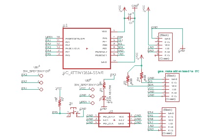
An interesting point I learnt is to used SPDT switch to represent 3 pins, it shouldn’t matter as we can also use pinhd as we just need the pads for the milling process.
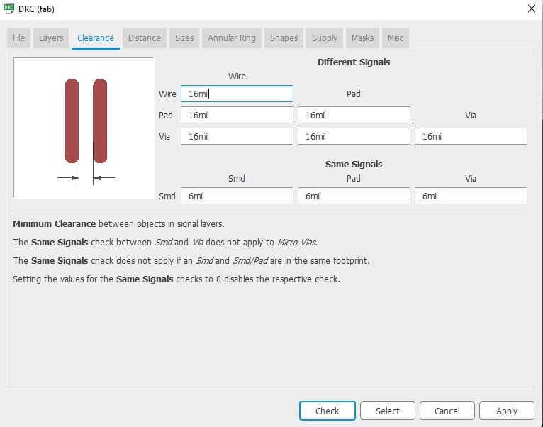
After designing the board, use ERC and DRC to ensure everything is correct
After that, just export the circuit’s traces and outline separately into mods and we can begin milling the gCode.
With that, I finalized the components to collect from Steven. However, that was also when an accident happened, which will be elaborate below.
| Part | Quantity |
|---|---|
| ATtiny1614 | 1 |
| FTDI 6 pin male header | 3 |
| FTDI 6-pin female header | 2 |
| Non-polar Capacitor 1uF | 1 |
| Resistor 10k Ohmn | 1 |
| Resistor 4.99k Ohm | 2 |
| Resistor 1k Ohm | 1 |
| ISP 6 pin SMD header (used as ground connections) | 1 |
| Push Button | 1 |
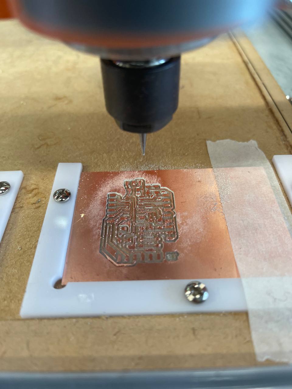
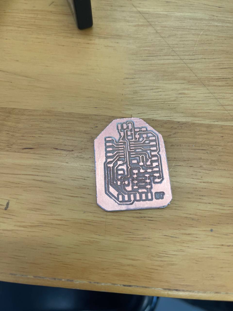
After checking, then we start to mill the board!
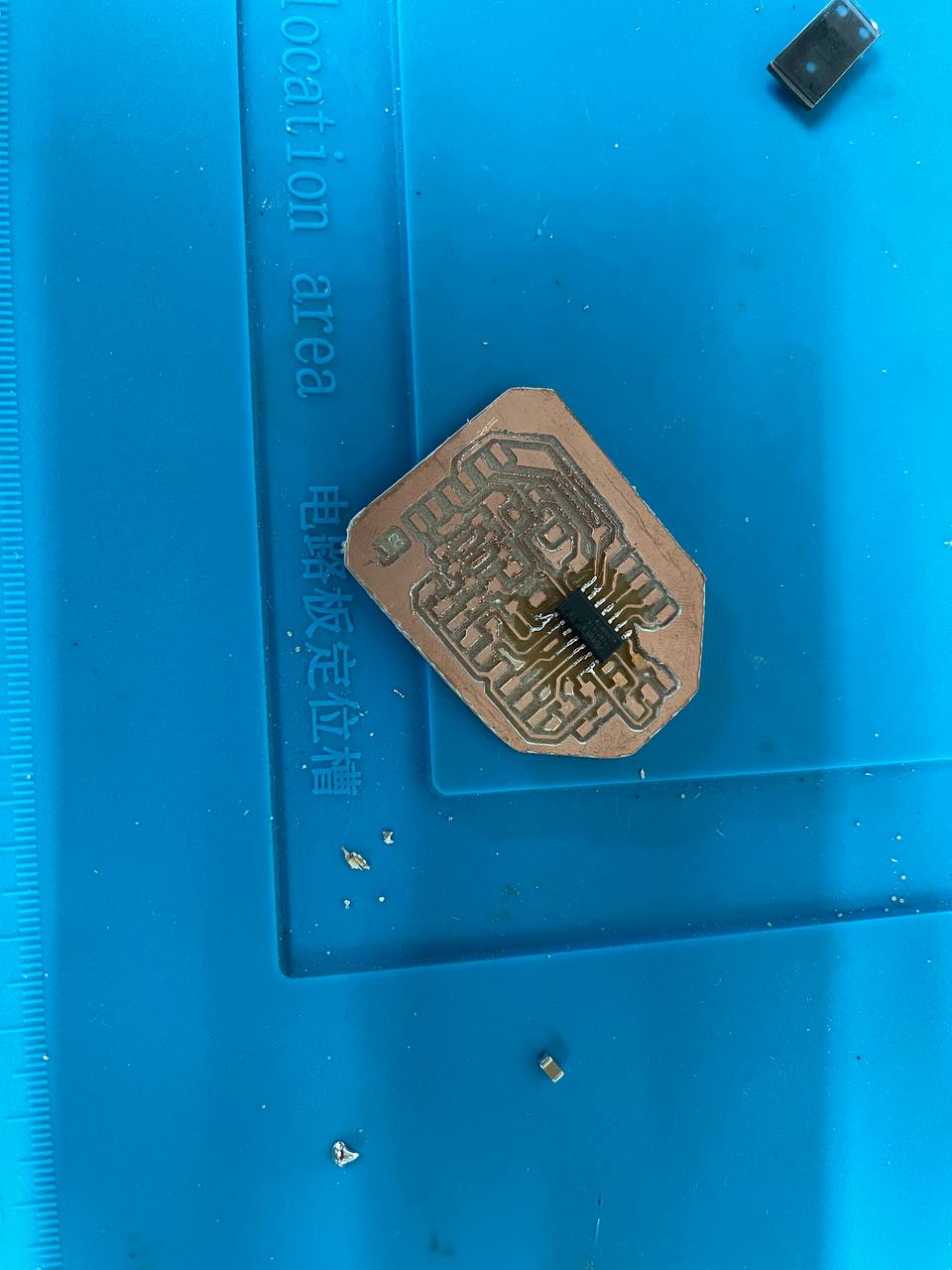
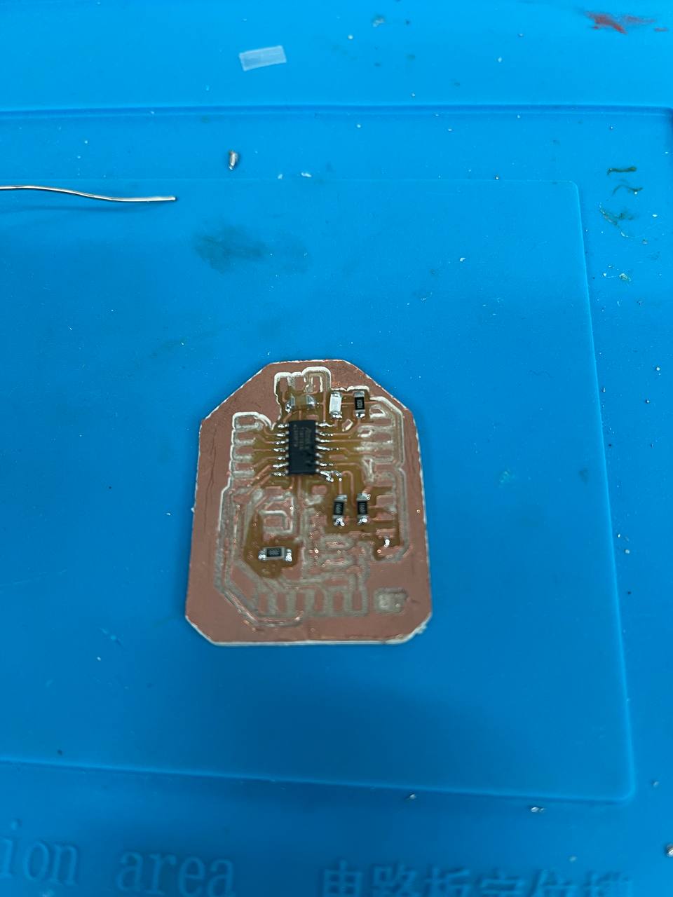
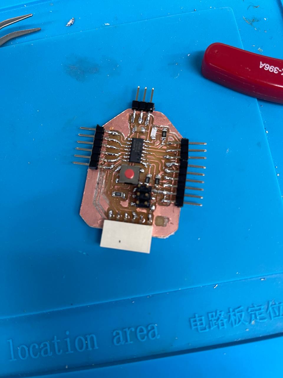
Soldering
Soldering was relatively straighforward in my opinion. Basically, the steps I took are as follows:
- Identify what component to solder first
- Put a generous amount of flux on its pad
- Solder, check that the part is indeed soldered onto the pad (continuity test is useful here)
- Rinse and repeat
To solder the parts, I took the approach to solder from low to high, and small to large components. Hence, this is the sequence I soldered in
- ATtiny 1614
- 1k Ohm and LED
- Other resistors
- Push Button
- FTDI male headers
- FTDI female headers
- ISP header (used as ground connections)
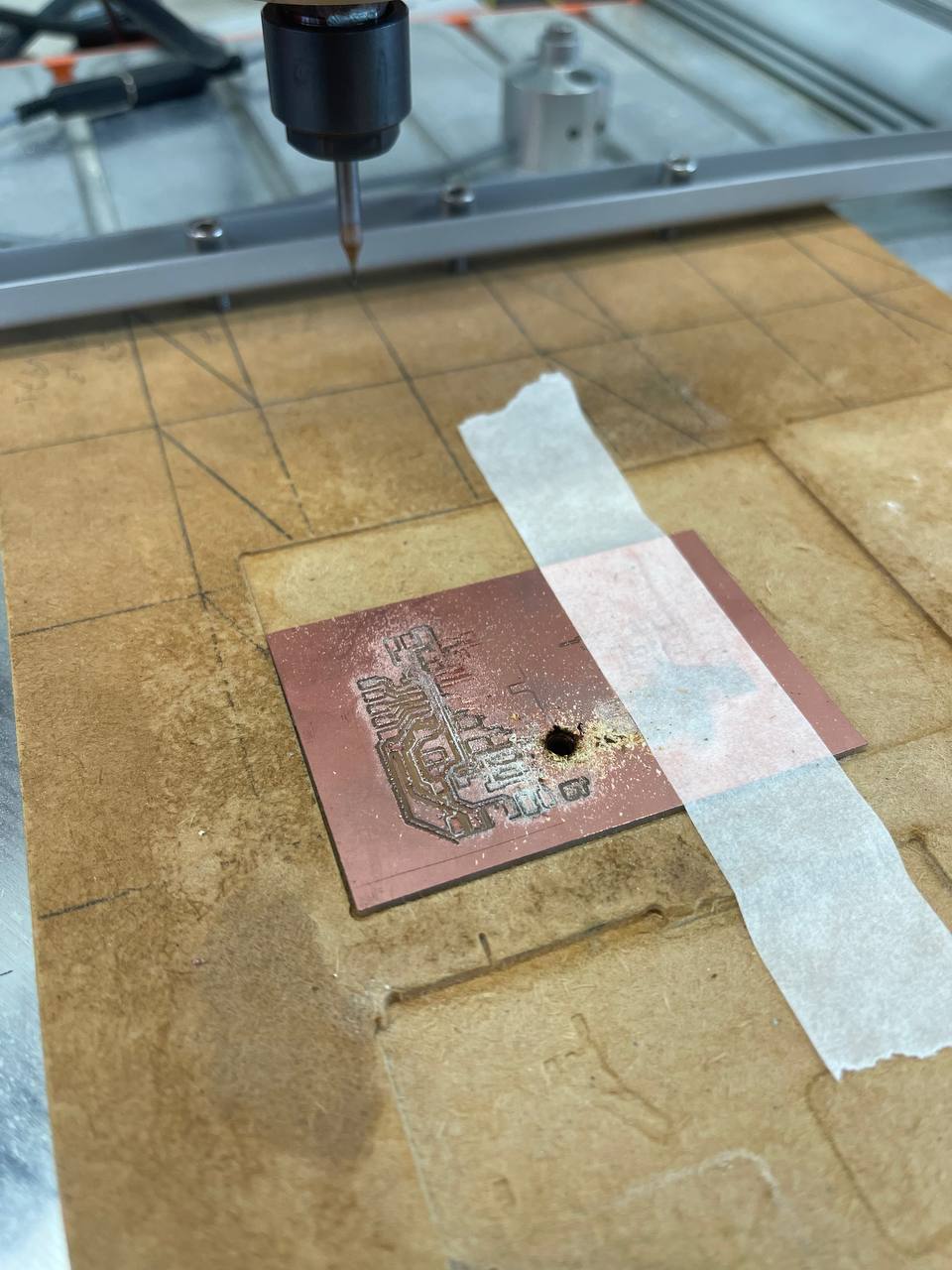
Here are some pictures of the process
Final Testing
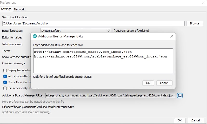
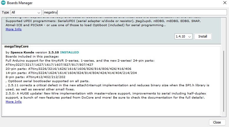
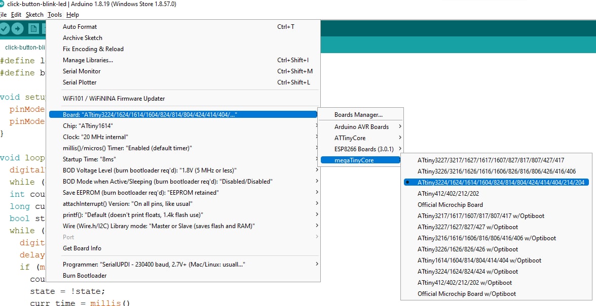
To test whether the board is working, we need to include megaTinyCore into Arduino IDE.
- Add
http://drazzy.com/package_drazzy.com_index.jsoninto preferences. - Download the library from board manager
- Select ATTiny1614 from available boards
- Burn bootloader (if needed)
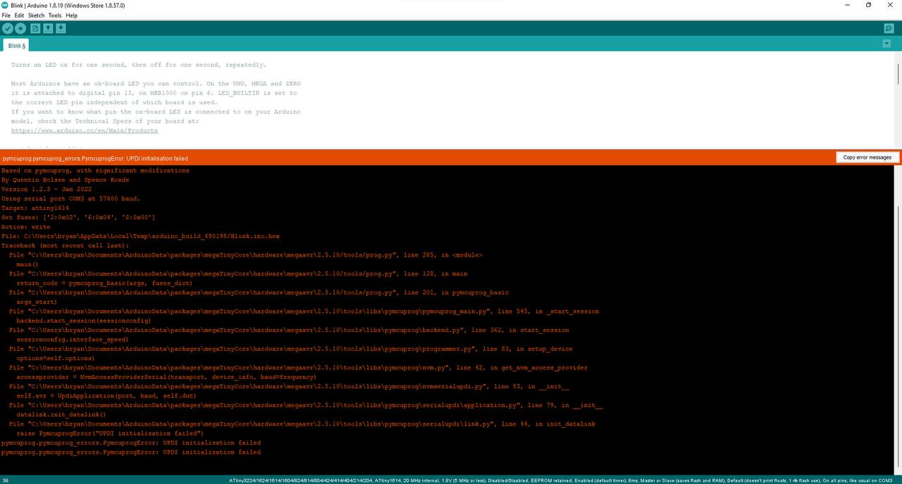
To do some testing, initially I tried to upload a demo program onto my hello_world board. This was not successful as my FTDI to UPDI adapter did not have a high enough resistor value when connecting the TX and RX of the FTDI-side signal to UPDI-pin (I soldered a 49Ohm resistor instead of a 4.99k resistor).
Fortunately, after that fix, I was able to upload a Blink program with modifications to see the LED on my board blinking. Here is the code sample:
#define LED 10 // PA3

// the setup function runs once when you press reset or power the board
void setup() {
  // initialize digital pin LED_BUILTIN as an output.
  pinMode(LED, OUTPUT);
}

// the loop function runs over and over again forever
void loop() {
  digitalWrite(LED, HIGH);   // turn the LED on (HIGH is the voltage level)
  delay(1000);                       // wait for a second
  digitalWrite(LED, LOW);    // turn the LED off by making the voltage LOW
  delay(1000);                       // wait for a second
}
Mistake
When I was using the CNC mill, there was some leveling issues with my board. To save time, I decided to adjust the Z-axis to mill deeper than usual. As per electronics production week, as we shift the Z axis up, it will be able to cut deeper. I lifted the Z-axis up to a value of 4.325, and I wanted to cut just slightly deeper, so I wanted to set it to 4.375, moved the progress of the gcode backwards to where it hasn’t milled through, and hit the start button.
However, as I was listening and checking the gcode running, I noticed a very deep cutting sound instead of the sound of slightly removing materials. That was when I knew something was off. I immediately hit the emergency button, hit the cycle stop button, and hit the reset button twice. However, I wasn’t able to move the mill head up, and it started to make a weird burning smell. Luckily, there were other lab technicians and students available that helped me stop the mill from further damage. I am super thankful for them, as I was practically in a panic state at the time.
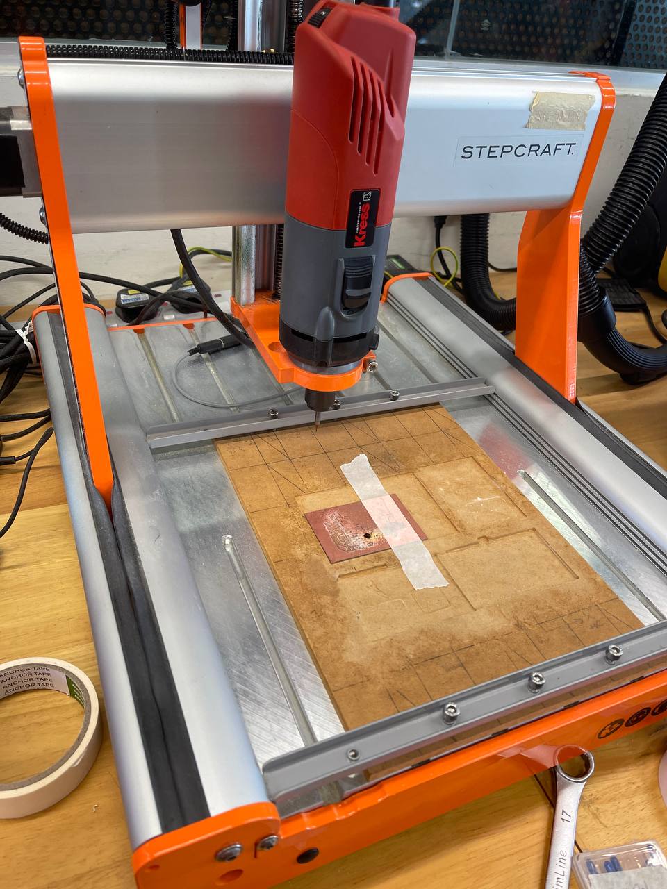
When we looked at the values on the Z axis, it was at nearly 42k! That meant that I did not follow the SOP of using the CNC mill, and just run the mill before checking and double checking.
I felt that this incident, while is a user fault, required stars of misfortune to align:
- Less adjusting values = less chance for mistakes made.
- When I was milling, the milling surface was slightly uneven, and it requires users to calibrate it before using. Somehow out of the 3 machines in the lab, I chose the one that Jonathan, fellow Fabacademy mate, had a lot of issues with last week as well. What I should have done is to either calibrate the milling surface properly before restarting my milling job, or just use a different machine other than the one I know had calibration issues (it was my second try for the same milling job).
- The software did not have invalid value checking.
- Somehow, the milling desktop application did not detect that I have set a value that the machine cannot reach (if that was the reason). For example, normal values on the milling machine is at most in the 100s range. Even if we take into consideration the actual machine coordinates vs the software view (which in my opinion is an offset applied), the values should at most only 2x times of the X, Y, Z axes; therefore the maximum values would be at most 1000-2000.
- To prevent user fault, perhaps it is better to implement a safety check between the the current offset to the max z axis position in the gcode initially, and perhaps have a hidden checkbox to allow advanced users to disable it if need be.
- Numbers flying around the screen
- As a person who has only used the CNC mill 2 weeks ago, and did not use it for a week, there were definitely some steps in the SOP that I have forgotten. I remembered the key parts:
- checking the start of XY axes
- zeroing the XY axes
- checking the Z axis calibration probe works
- always calibrate z axis when changing an endmill
- ensure the f4 board has adequate adhesion with the milling surface and push it down as much as possible
- There were a lot of numbers on the screen, yet there wasn’t a design emphasis to ensure users can focus on specific windows. Perhaps there could be better spatial separation between the different sections on the screen and more annotations so that users know what they are looking at whilst the machine is operating. Potentially better placement for the various sections in CNC milling app’s layout?
All in all, this incident highlighted to me the importance of following and sticking to an SOP! In fact, it might even be better to fine tune these SOPs and present them formally for all users of fablab to adhere to. This reminded me of various final projects that actually implement the concept of reminding people how to use various tools in the lab, and I have definitely grown to appreciate them more. Although this incident made me incredibly disheartened in using a CNC mill, for some reason I am more eager to use it and learn from my mistakes; sometimes theoretical problems are easier to forget, but to experience this firsthand has left me an impression that I will never forget. I definitely still want to mill things, not only because it is an incredibly powerful process, but it is also a fruitful one.
Mistakes have been made, lessons must be learnt, and improvements must happen.
Conclusion
While this week I had made/noticed a lot of mistakes from previous week, I was extremely grateful to be able to experience this. I will be more careful when using the machines from today onwards.
Design files
- Redrawn ATtiny 1614 board schematic board components traces outline