9. Embedded programming
This week I learnt how to read datasheets of microcontrollers and tested my microcontroller by writing some programs.
Overview
As I am a Polytechnic Graduate, and currently enrolled in NUS’s Bachelor in Computer Science, I am no stranger to programming. I have programmed some Arduino UNOs before using the Arduino IDE, in Arduino (Wow that’s a lot of Arduino!).
The above sentence was possible, as what professor Neil mentions that Arduino can mean many things, from the Arduino Company, Arduino Integrated Development Environment (IDE), Arduino language which is a derivative of C, the Arduino board design which is open source, etc. Whever possible, I will try to be as specific as possible.
- Read datasheet for ATTiny1614
- Use UPDI programmer to program ATTiny board to do something
- Try AVR GCC
- Compare performance and development workflows of other architecture
- Programmed the board to do something
Group Assignment
For this week’s group assignment, we are supposed to compare the differences between performance, specifications, as well as the different workflows for other architecture. It was truly an eye opener to compare these different workflows.
View group assignment here.
Understanding the ATTiny1614
The datasheet for the ATTiny1614 is nearly 600 pages long. Just looking at the features list was super overwhelming. THis is because I did not know what these metrics corresponds to in terms of creating a system.
Some of the questions I had:
- Does a different architecture make a difference in terms of performance? Or is it just a different way to “making a chip”
- I understand that (generally) the higher the clock speed, the faster the program runs. However, is there any way to know before hand what kind of “performance” I would need purely from reading the datasheet?
- What is: SIngle-cycle I/O access, Two-level interrupt controller, Two-cycle hardware multiplier?
- How much is 16KB Flash memory? How many lines of code (LoC)?
- How does a Brown-out detector work?
- How should we activate sleep mode for ATTiny1614?
All these questions stem from a fundamental question: What processor is best suited for my application?
And the answer to that is simply: RTFM
Lucky for me, my instructor Steven recommends us to read the FUSE, Registers, PORTMUX, PORT I/O configurations, CLKCTRL, USART, ADC and DAC sections as a start. Although that is still a lot, I think it would definitely be a lot better than just blindly reading parts that are irrelevant.
- Block Diagram
- FUSE
- PORTMUX
- PORT I/O configurations
- CLKCTRL
- USART
- ADC and DAC
My goal in reading the manual is not to be a master of ATTiny1614, but a master in understanding any manual that is thrown to me in the future, or at least know how to navigate around the manuals.
Block Diagram
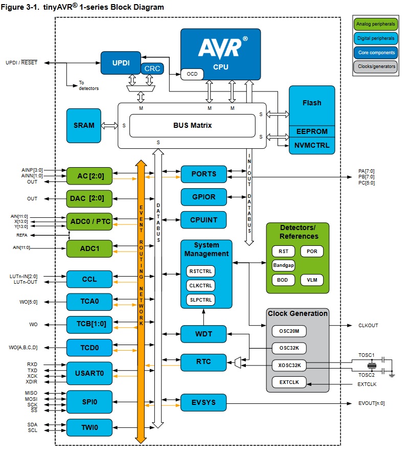
As per mentioned in Professor Neil’s class, microcontrollers (and other devices) are following the Harvard architecture. THis was different from Von Neumann architecture in that Harvard Architecture stores program memory and data in separate memory segments. The image below is from this site.
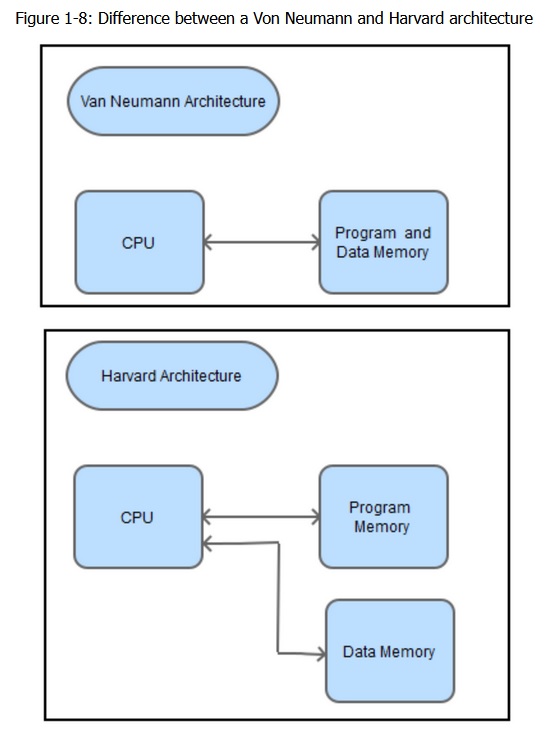
We can clearly see that Flash, EEPROM and NVMCTRL are separate entities from SRAM, showing that it is Harvard Architecture.
Pinout
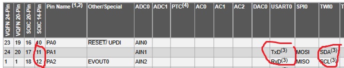
As per previous weeks, I am using ATTiny 14-Pin SOIC. The following is the pinout:
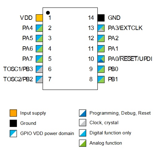
That’s a lot of details, but essentially:
- Power supply connects to 5V to Pin-1 and GND to Pin-14
- Apply external clock to Pin-6 and Pin-7
- Each pin other than Pin-6, Pin-7, Pin-1, Pin-14 have analog functions
- All pins use the same power as VDD (same power domain)
- Use Pin-10 to do UPDI programming
But, that isn’t the full picture. Looking at the datasheetfor multiplexed signals, we see some very intersting things
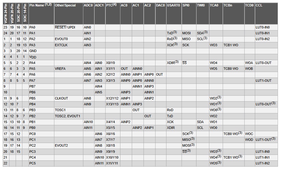
The key takeaway here is:
- It is possible to design a board with alternate pin positions in mind
- As per datasheet, all pins can be used for external interrupt, no idea what does full asynchronous detection mean but I would love to experiment it someday
- One pin can be connected to multiple peripherals
- For example: AC pins share the same pins as ADC
I was confused what the difference AC and Analog Convertors. After asking Steven, AC stands for Analog Convertors, and ADC stands for Analog to Digital Convertor. The former compares two voltages and returns either a high or a low, while the other takes in an analog signal and converts it to 2^n levels based on how many bits the ADC has.
I was extremely confused, as initially I thought that each pin on the SOIC had only 1 function, but it turns out each pin can in fact be an interface to multiple peripherals. After clarifying with my instructor Steven, the usage of these pins can be planned out, and if there is a need to we can technically make boards or write software to multiplex some signals to be fed into both peripherals through the same pin. If we need to use these peripherals, but prefer the peripherals to be decoupled, it makes more sense to choose a different chip rather than racking our brains to make it work (unless unnecessary).
PORTMUX
Multiplexing is the concept of allowing multiple things “combine” into one following certain rules with no loss of information. It’s complement is usually accompanied, demux, where a single signal is also distributed across many signal lines.
Based on this definition, PORTMUX would mean that a single port would have multiple functions. The overview in the datasheet explains that PORTMUX either enable or disables functionality of pins, or change between default and alternative pin positions, and is specified in the PORTMUX register map.
These are the things that can be changed:
- CCL LUT 1 & 2 (Look up Table)
- EVOUT 0, 1 & 2
- TWI0
- SPI0
- USART0
- TCA00-05
- TCB0,1
In more “useful” terms:
- CCL stands for Configurable Custom Logic. Details about it can be found on point 28. Based on the table above, the Look Up Table has 3 bits, number of entries is 2^3 = 8 entries.
- TCA and TCB stands for (Timer/Counter Type X), and these are basically PWM pins, which means that the ATTiny1614 has a total of 6 PWM pins. Doing a quick google search and we find a tutorial on Timer/Counter programming guide by microchip
- TWI is used for I2C interface, we can set the I2C interface to alternate pins
PORT I/O Pin Configuration
The features of I/O configurations are as follows
- GPIO with individual Pull-up and Invertible I/O
- Interrupts and events which are able to detect sensing of both edges, rising, falling, and low-level edges
- Async Pin Change sensing that can wake device from all sleep modes
- Hardware Read-Modify-Write through dedicated toggle/clear/set registers and use of virtual ports
As per teachings of Steven, each of these PORTs have 3 important bits: Data Direction (PORTx.DIR), Data Output Value (PORTx.OUT) and Data Input Value (PORTx.IN). The process to use the pins are essentially
- Initialization
- After resetm all outputs are tri-stated, and digital input bufferes are enabled even if no clock is running.
- Operation
- There are details on how to use it at a low level. Setting PORTx.DIR register to ‘1’ allows the pin to be an output.
- Writing a PORTx.OUTSET bit to ‘1’ will set the corresponding bit in the PORTx.OUT register to ‘1’, while ‘0’ to clear the output.Writing a bit in PORTx.OUTTGL or (strangely) PORTx.IN would toggle it.
- To set it as an input device, setting PORTx,DIR register must be written to ‘0’ to disable the output driver.
- Functions
- Peripheral Override: peripherals can be configured to be enabled, of which the PORT will be overridden in a perpheral dependent way. In peripherals, they might have different PORT behaviours, therefore it is worth reading the datasheet on these information.
- And many, many more…
The registers here are important to read up if I were to resort to writing in AVR GCC instead of Arduino.
CLKCTRL - Clock Controller
This section shows that There are 2 internal oscillators, OSC20M and OSCULP32K. There was also something called the Prescaler, which further decreases the clock speed. This can become important if we are to make low powered systems.
For the internal Oscillator, there are 2 center frequencies, which are 16MHz and 20MHz. The oscillator comes with factory calibration, but we can fine-tune it by using a timed write procedure to change the main clock and prescaler settings.
Configurable Custom Logic (CCL)
This is a link that I found about CCL.
Memory Section Access from CPU and UPDI on Locked Devices
At section 6.9, the datasheet mentions that ATTiny1614 has a FUSE.LOCKBIT, which prevents application data to be read out via a debugger tool. However, the datasheet mentions that “…Regular memory access from within the application is still enabled…”, which implies that if we do not write security related things onto the TxD and RxD lines, we should be safe as hackers cannot get the application data directly.
This reminded me of a reverse engineering project I read up during an IoT Security class, where Device EUI, Application EUI and App Key was compromised through reading from TxD and RxD of the chip in a employee monitoring PIR sensor. Check out this article for more information.
FUSEs
FUSEs are part of nonvolatile memory and hold the device configuration. FUSEs can only be set via UPDI, and cannot be set by CPU.
There are a couple of Configurable FUSEs:
- Watchdog
- Brown-Out Detection
- Oscillator
- TImer Counter
- System 0, 1 configs
- Application Code End
- Boot End
- Lockbits
Even after reading much of the contents in the datasheet, I do not find it very useful, but I believe its usefulness will come in time. I did however, find this particular forum post about someone’s ATTiny1616 FUSEs being bricked.
USART
There were a lot to unpack when reading the datasheet. Practically speaking, the key thing to note is the existence of 2 alternative USART pins. In fact, doing this allows for a high degree of flexibility, as the alternate pins for USART is actually the same pin for alternate pins for TWI/I2C.
Next, the transmission (TX) of the microcontroller will need to be received (RX) by another device, and vice versa. Hence, it is common to connect the TX to the RX of another device, and vice versa. This is especially important in circuit design.
Testing the ATTiny1614
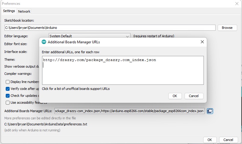
To compile code for ATTiny1614, we must include the board from board manager. See Electronics Production for details on how to do that.
We can use the ATTiny1614 either in an easy way or the hard way.
To start off, I decided to use Arduino IDE to programme the board. In fact the simplest form of example would be to use the blink program with some minor modifications as per week 6.
#define LED 10 // PA3

// the setup function runs once when you press reset or power the board
void setup() {
  // initialize digital pin LED_BUILTIN as an output.
  pinMode(LED, OUTPUT);
}

// the loop function runs over and over again forever
void loop() {
  digitalWrite(LED, HIGH);   // turn the LED on (HIGH is the voltage level)
  delay(1000);                       // wait for a second
  digitalWrite(LED, LOW);    // turn the LED off by making the voltage LOW
  delay(1000);                       // wait for a second
}
We analyze what is going on by diving deeper into some of the function calls:
pinMode: Setting if a pin should be inINPUTorOUTPUTmode.digitalWrite: Setting the pin’s corresponding register value to eitherHIGHorLOWdelay: Sets how long to wait before executing the next line of code. Blocking operation.
A similar analysis can be done to understand the push button example:
digitalRead: Gets the value in the pin’s corresponding registerSerial.begin: Sets the baud rate of hardware serial on the ATTiny1614Serial.println: Prints data to the serial port as ASCII text followed by a carriage return\n
This is technically sufficient to complete the assignment for the week. However, I wanted to learn a little bit more about what is going on at a lower level. Credits to Steven for showing me how to write an equivalent AVR-GCC version of the blink program.
/*
 * Blink with (avr-gcc)
 */
#define F_CPU 3333333
#include <avr/io.h>
#include <util/delay.h>

#define led  PIN3_bm

int main(void) {
  PORTA.DIRSET = led;
  while(1) {
    PORTA.OUTTGL = led;
    _delay_ms(250);
  }
}
How the program works is as follows:
- Define the frequency of the CPU taking intop consideration prescaler. Prescaler makes the timings more fine.
- Incldue
avr/io.h; ifdelayis used, importutil/delay.h - In the main function:
- assigning
PIN3_bmtoPORTA.DIRSETsets the state of dataflow between the pins - Create a loop which toggles the infor in the register (instead of setting it to high then low manually) using PORTA.OUTTGL
_delay_msis used to block the program for the specified milliseconds.
Some additional things to note here:
F_CPU: if not specified, the compiler might take a value when calculating time intervals. This is because each “cycle” is directly related to the operating frequency of the CPU.PIN_bm: this macro makes it easier to define the input/output pins. This corresponds to modifying PA3 settings on ATTiny1614.
Other than this, Steven has also shown me the effects of setting F_CPU incorrectly:
INSERT VIDEO OF BLINKING AT WRONG TIMING HERE
To simplify the writing of AVR-GCC, an IDE such as ATMEL Studio could be used.
Individual assignment
After contemplating the differences between AVR-GCC and Arduino, I find that using Arduino sacrifices performance, but should be invisible given a feature such as blinking an LED. As such, simplifying the process I decided to use Arduino to write this blinking of LED.
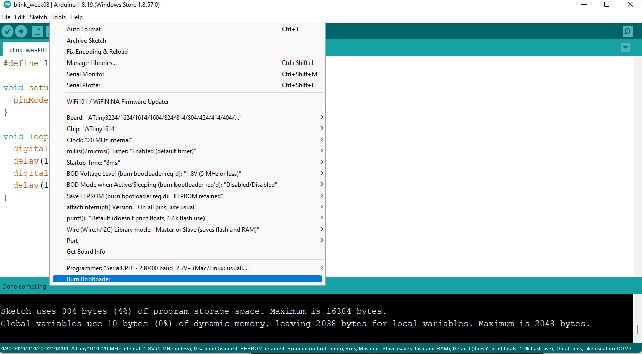
Compiling
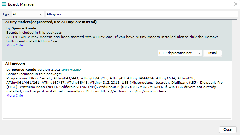
Before compiling the code, we need to specify the use of SpenceKonde’s ATTiny library.
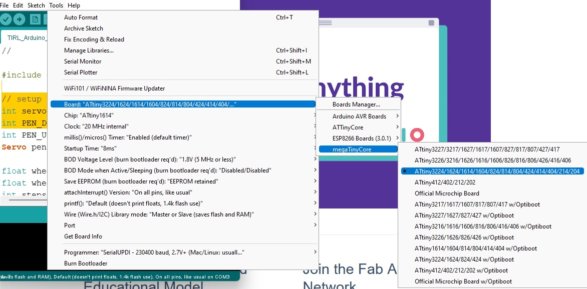
Next, select ATTiny1614, and keep everything else as default.
Burn the bootloader to the microcontroller.
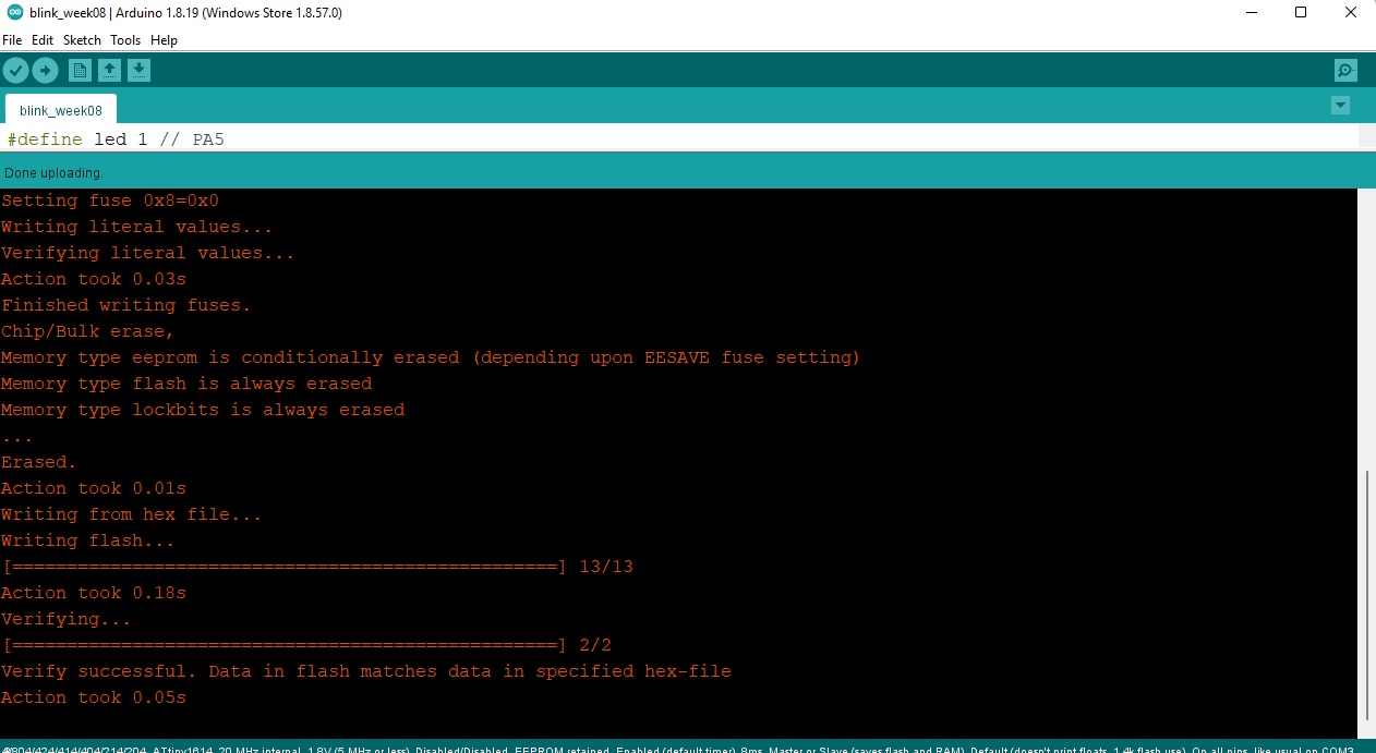
Uploading
We are doing UPDI programming. Connect the UPDI pin of the ATTiny1614 to the FTDI-to-UPDI adapter board, then connect the VCC and GND between the boards as well.
Next, click the upload button. We will see something similar to below
Result
Files
- Final blink code .ino