5. Electronics production
This week I worked on fabricating my own programmer.
The goal
I decided to structure my documentation a bit better from now on. Mainly, I want to have a simple to do list here so that I can refer to it and ensure I have complete what is required and what I want to explore (sorry if it sounds a bit too pragmatic!).
- Understand what is an in-circuit programmer
- Characterize lab machine
- Fabricate board
- Solder components to what was created
- Program the programmer/ensure the device is recognizeable by our computer
- Testing
What are in-circuit programmers?
TLDR: In-circuit programmers are useful to reprogram chips after they are soldered onto a board, as usually that means they are closed-off from users.
Based on my understanding, circuits are seen as a “closed” ecosystem; once things are in, there shouldn’t be a way to change it anymore. Say that we want to make a 3D printer to be sold, I would choose interfaces say through a touch screen to select what to 3D print, and use Wifi or an SD card to send the STL files to be printed to the 3D printer. As such, there would be no need for me to have headers for the devices to be reprogrammable, and my circuit can have a much smaller footprint. A similar argument can be made for wearables. We wouldn’t want a USB port poking out of, say, an earing right?
In-circuit programmers to the rescue! Basically, these nifty devices allow a device to be used reprogrammed should a bug be detected, or if the circuit is to be reused. This leads to an interesting thought, and also links to the FabacademyMeme that I saw a couple days ago: If we collected all in-circuit programmers in the world, and know exactly what pin goes where in order to reprogram a chip, does that mean we can harness the power of any chip available in the world?
Getting the bigger picture
During the weekly lesson review, I probably asked more than I should have. Regardless, here is my understanding of the key points mentioned.
- What are the traces about?
- Those are used to see how deep and how well the lab drills would work. Based on the results, you can know how to use the machines in the lab to tailor make your designs. Although there are theories on how to use mill, in reality machines have thier own characteristics and we need to design around them. Use your machines, don’t fight with them.
- What are the sizes I should know about?
- Mainly 1/64”, 1/32”, 100 mil. Roughly speaking, 1/64” is 0.4mm, 1/32” is 0.8mm, and 100mil is roughly 2.54mm. Normally, use 0.4mm endmill to make your traces, and 0.8mm endmills to cut the outline of your board.
- Do I need to design my own board this week?
- It’s not mandatory, as week 6 we’ll be redesigning a Hello World board to minimally add some buttons and LED switches. It’s good however, to be aware of it early on.
- Why do we need to send the UPDI boards to board houses?
- It’s good to know the process of handling board houses. It is however, not required to do so, as we can learn when we are custom making our own PCBs.
- There are so many types of PCB to choose from! What types of board should we use in the lab?
- We will be using FR1 as it is easier to mill in labs
Characterize lab machine
As part of the group project, we have decided to characterize the machine through the use of the trace width tool. The CNC mill in our lab is by a local brand called Stepcraft.

We used the linetest trace, and this was the result:
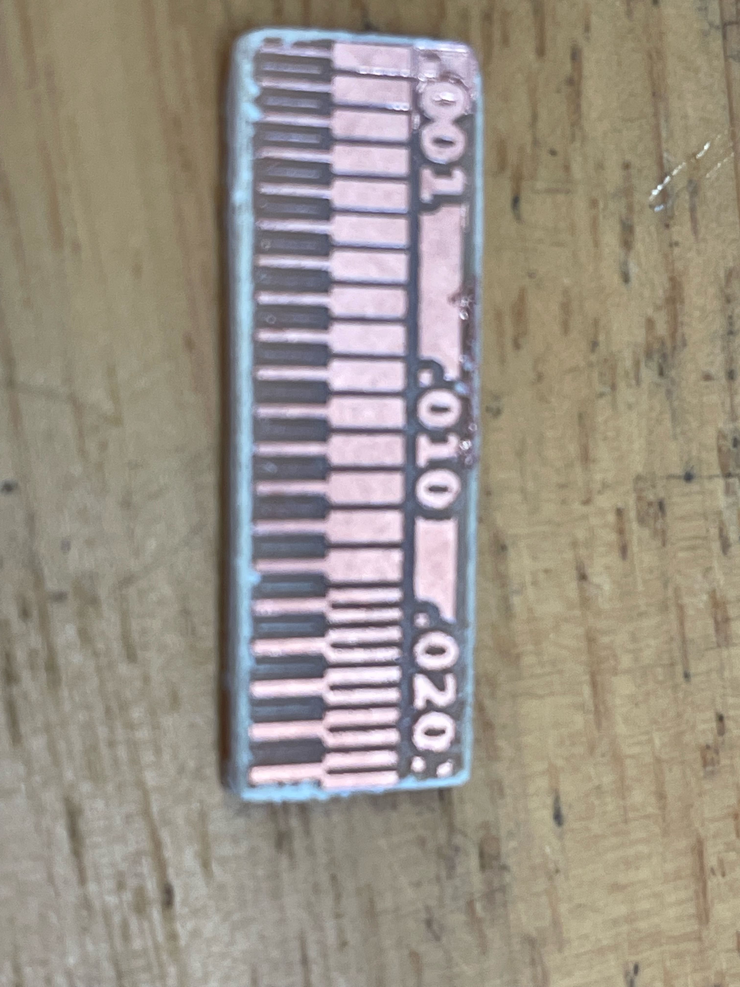
The key take away are as follows:
- Our lab uses V-bits for tracing as it is cheaper per bit.
- Our lab uses flat endmills for outlining, as the depth throughout the cut of the PCB should be the same.
- To cut thinner lines, as Professor Neil mentions in class, the width of the trace is a function of the depth of cut. Therefore, it is important to do a rough estimation. We can use basic trigonometries to get the theoretical depth-of-cut, and fine-tune from there on. Thinner lines require less depth of cut for V-bits
- Generating
.ncfiles via mods is super convinient! - Using double sided tape does not always yield consistent adhesion to the base of the cutting area. Always check and double check before cutting.
Fabricate board
Milling the board for me was quite a challenge, but was a fun and fruitful journey.
Firstly, I learnt that it is important to adhere the bottom of the PCB as securely as possible to the PCB, otherwise it may slip off the cutting surface, thus causing unnecessary wastage.
Next, I learnt how to properly calibrate and use the cnc mill. This will be useful for the future weeks! For our lab, we try to not cut too deep into the cutting board at the bottom, and ensure the next person can use it with as little friction to start as possible.
Below are the general steps I took to mill a board
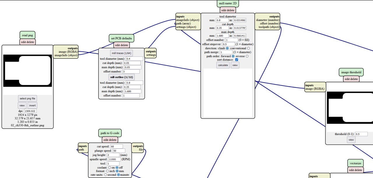
- Make/Download ready traces (as png or make Gerber->FlatCAM->png/nc file)
- If we have png file, upload into mods to generate
.ncfile. - Prepare PCB. For me, that meant to apply some double sided tape to the bottom of the PCB, and check that it can adhere securely on top of the milling surface
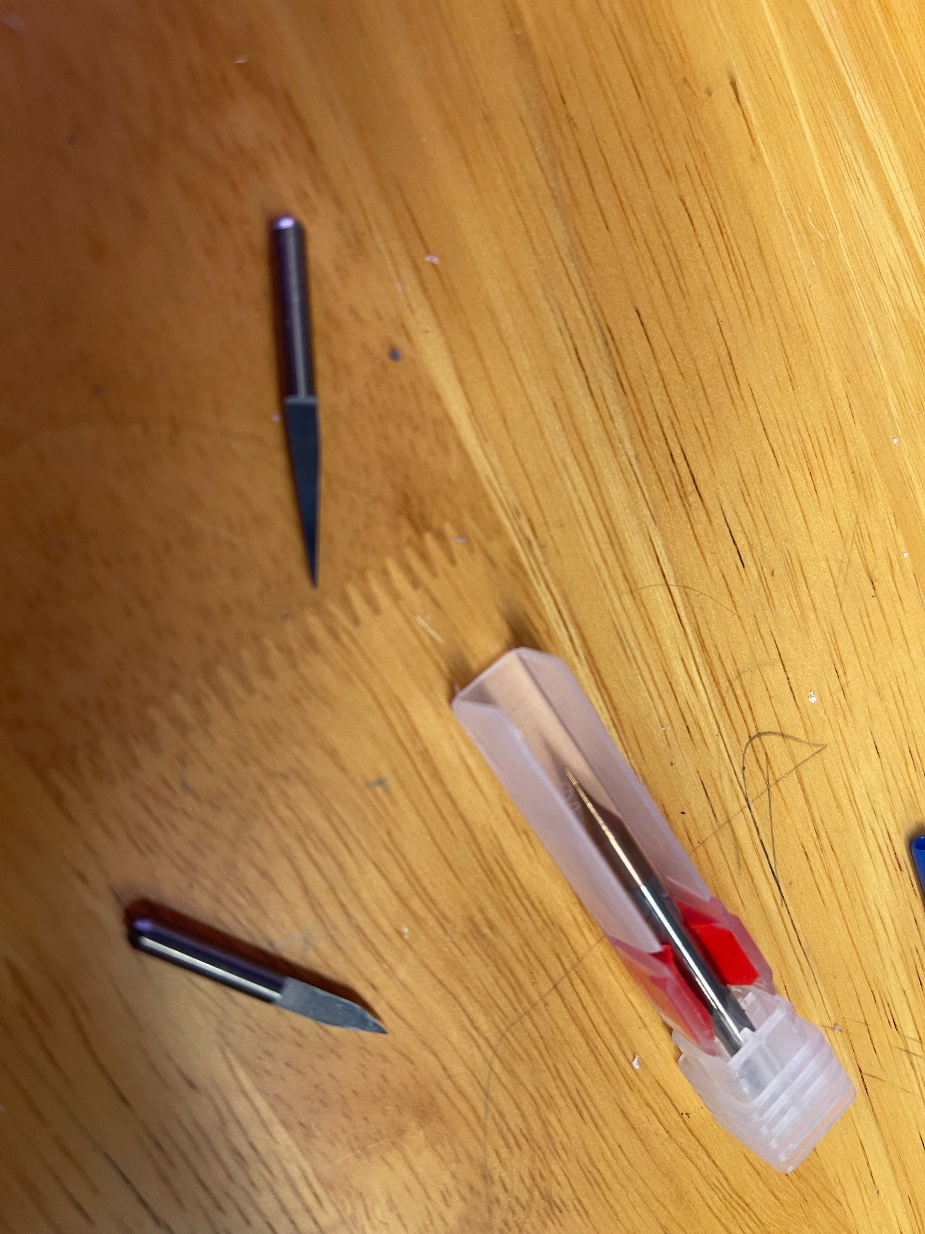
- Install V-bit into the collet.
- Calibrate the z-axis of the cnc mill
- Go to as far as the edge/corner of the PCB you wish to cut, and set the x, y axis to be 0 there.
- Load .nc file
- Do another check, make sure the endmill bits are tightened appropriately (wrist-tigth?), x, y are zeroed, z is mostly calibrated, have a vaccuum in hand to check the mill progress later on
- Mill!
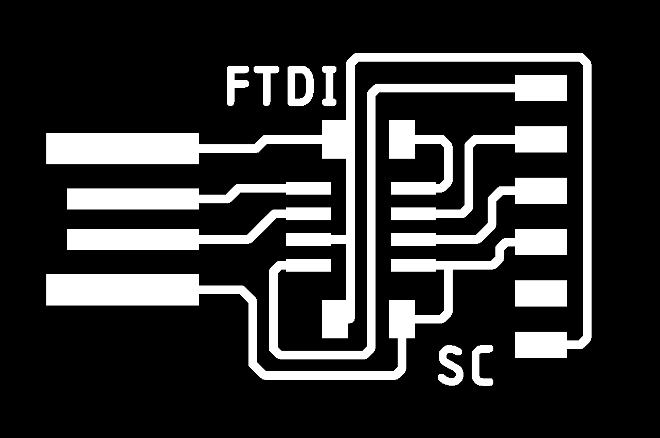
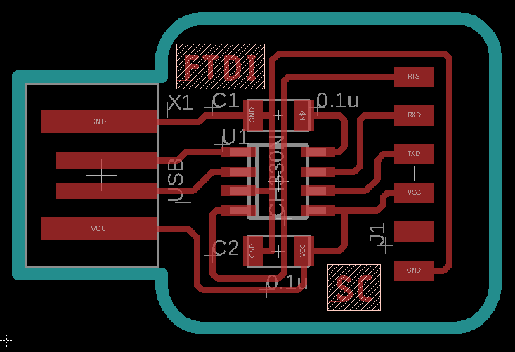
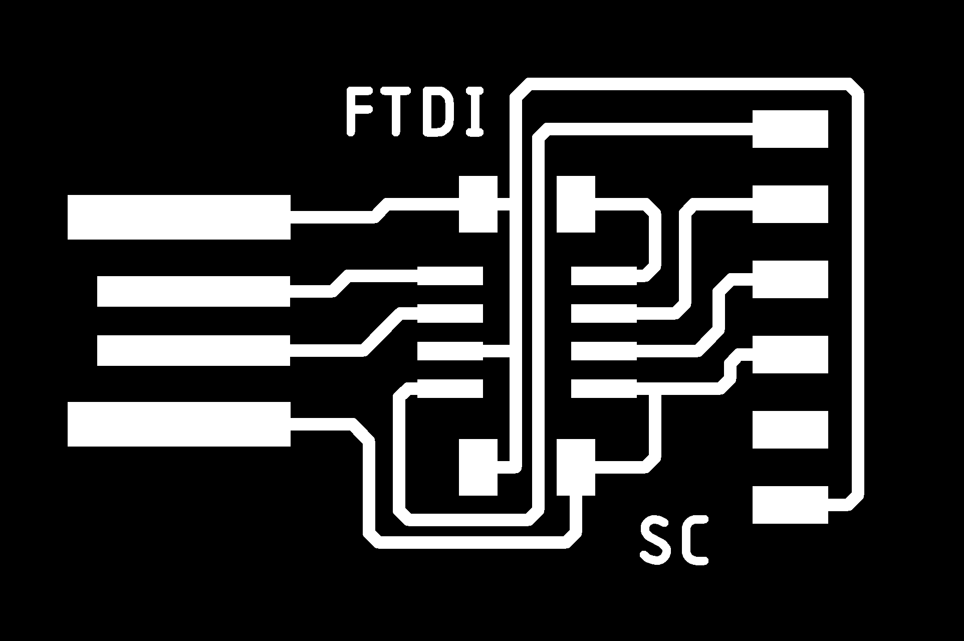
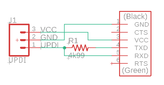
For me, I have decided to use my instrcutor, Steven’s design for FTDI board as well as FTDI to UPDI adapter board.
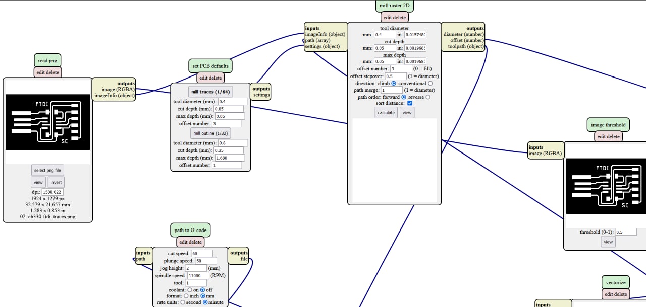
Generating the Gcode to be used in Stepcraft was intuitive with the help of mods.
Some important parameters for generating traces are as follows:
| Parameter | Value |
|---|---|
| tool diameter | 0.4mm |
| cut depth | 0.05mm |
| max cut depth | 0.05mm |
| offset | 3 |
| spindle speed | 12000RPM (roughly at 2 on Kress tool on Stepcraft) |
Meanwhile, parameters for generating outline are as follows:
| Parameter | Value |
|---|---|
| tool diameter | 0.8mm |
| cut depth | 0.35mm |
| max cut depth | 1.68mm |
| offset | 1 |
| spindle speed | 12000RPM (roughly at 2 on Kress tool on Stepcraft) |
After milling, there are some burrs around the outline. I used a Fine grit sandpaper to remove them from the board (similar to doing it in the group assignment).
Here is the reuslt of my milling
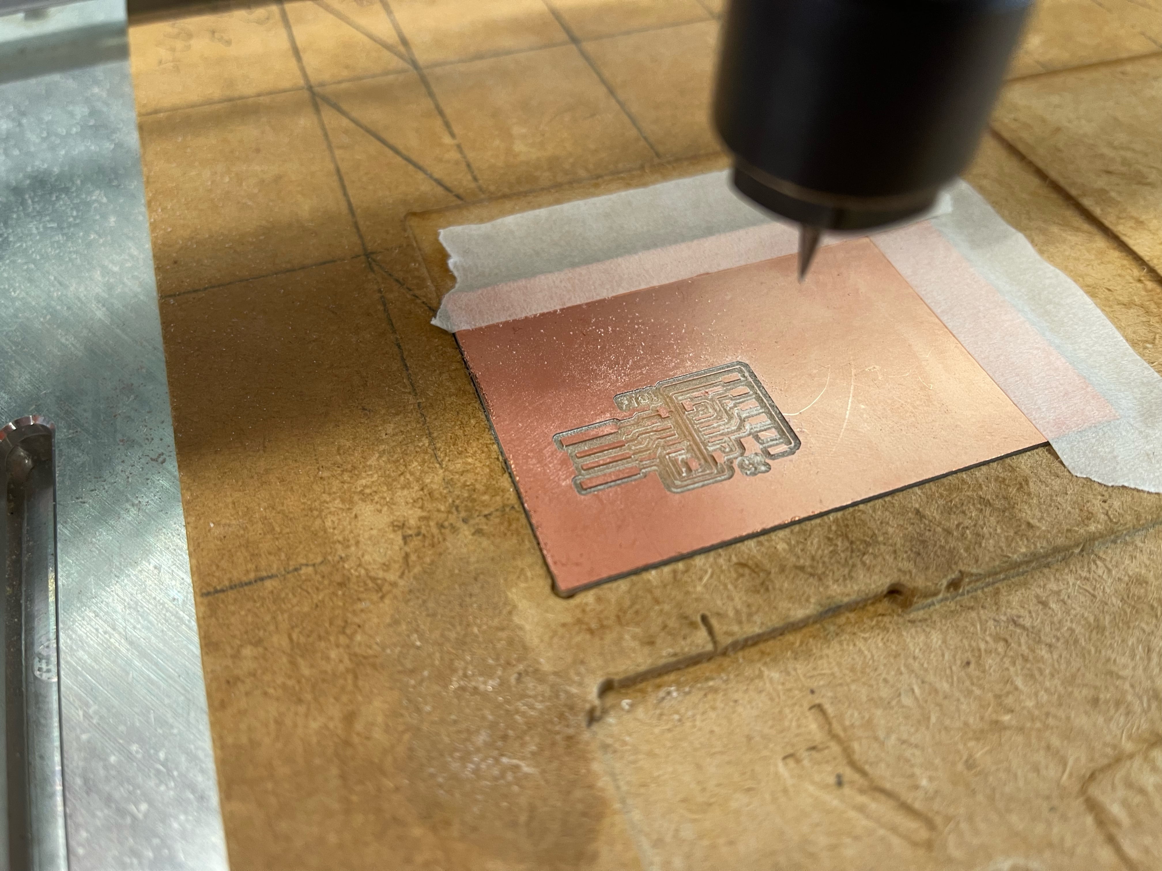
As far as I can tell, I think my traces were a bit too thin. Perhaps one way to go about it is to reduce the depth of cut, or use a 10 degree V bit instead of the 20 degree one. Regardless, it doesn’t affect it’s functionality.
Soldering components
Soldering the components are pretty straightforward (in theory), but is much more difficult in practice. I have soldered some through hole components in the past, but have never tried surface mounted components.
Things we need (credits to Steven’s student, Justin, for teaching me the ways!)
- Flux
- Tweezers
- Solder
- Soldering iron
The components to solder:
- FTDI board:
- CH330N x1
- 0.1uF x2
- FTDI-to-UPDI adapter:
- 499ohm resister
The general idea is:
Use flux! Get one leg of the component in place with flux and solder, and do the same for diagonal side. Then work your way through the other parts :)
It was impossible to take pictures while soldering. Generally, we should
- Solder the shorter components first. This means to solder in the SMD devices, then TTL devices, then the pin headers.
- Apply flux to where you want to solder. Put a few dabs of flux near the traces, as it helps to flow the solder.
- For SMD components (in my case there is only the CH330), solder in one leg first, then solder in the diagonal leg. This initial solder doesn’t have to be perfect, as it serves as an anchor for the second leg (which needs to be as good of a solder joint as possible)
- work your way around the component and in the end, return to the first leg and reflow it if need be
- A technique I learnt when soldering TTL components is to solder alternative pins, as we maximize amount of space to solder with no obstruction
- Repeat until all components are soldered. Do a connectivity test to ensure no circuits were accidentally shorted.
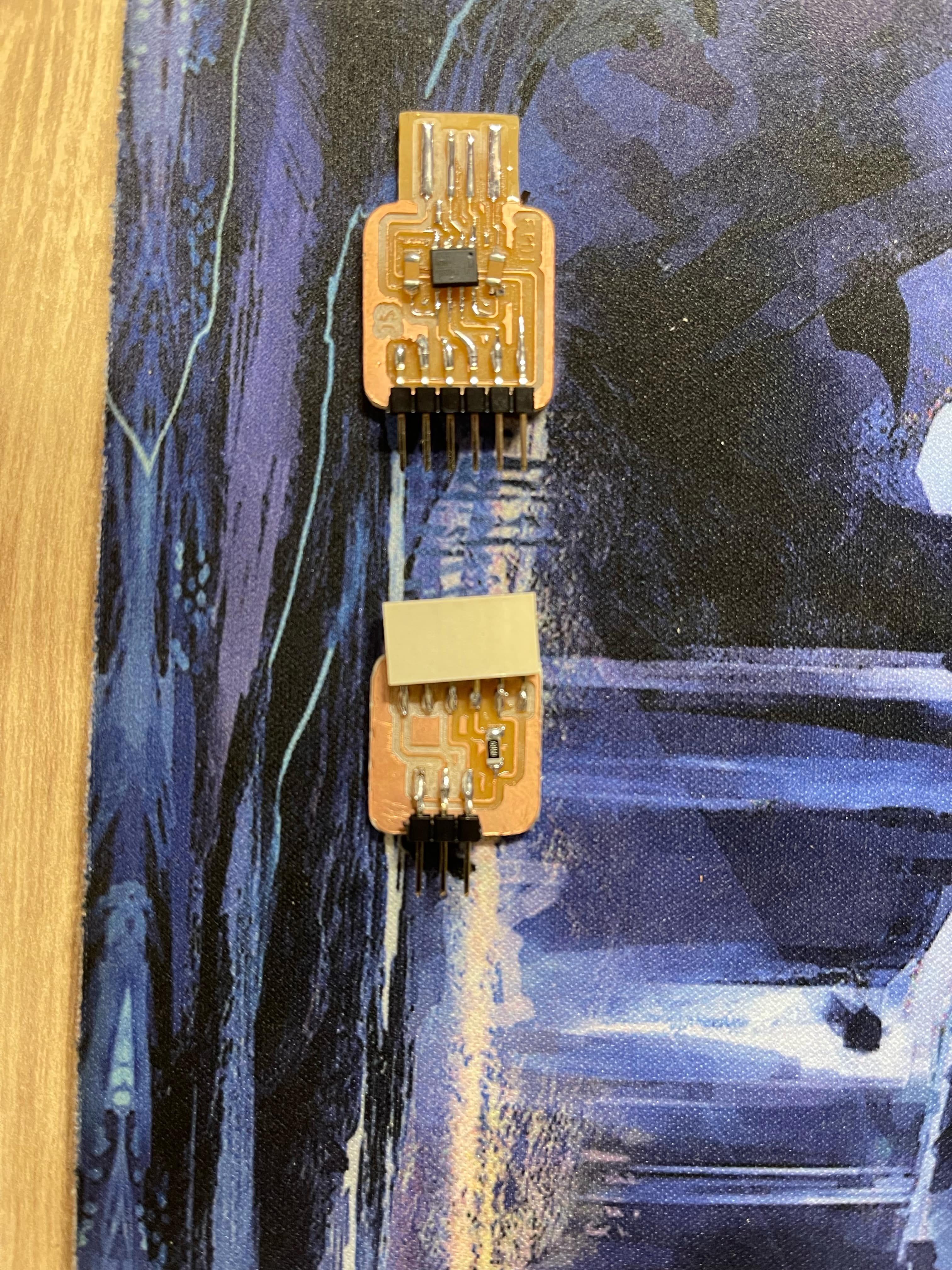
For this board, we need to ensure no shorting occurs. To do that, we need to manually strip away the cooper parts in the USB-esque header portion. This is done using a penknife or exacto knife.
Here is the result:
Ensuring FTDI is working
CH330N chip does not need to be programmed per se. However, as this is a new Windows laptop, I do not have any CH330/CH340/CH341 drivers installed. As such, I went to the FTDI website to install the required driver
However, after installing the drivers, I still could not locate my device. I was worried that the device had been shorted somewhere or the connection was not stable for some reason. I tried the “demo” board which was known to be working, and I still noticed my computer could not detect it.
I later found out that you can see COM ports connected to your computer. However, upon going to device manager, you will need to go to View > Show hidden devices. From there I saw that there was a greyed out CH340 device under my com port, indicating that my device had seen and recognized a CH340 device. This means that at least one of the boards (mine or the demo board) is working, and the drivers are properly installed.
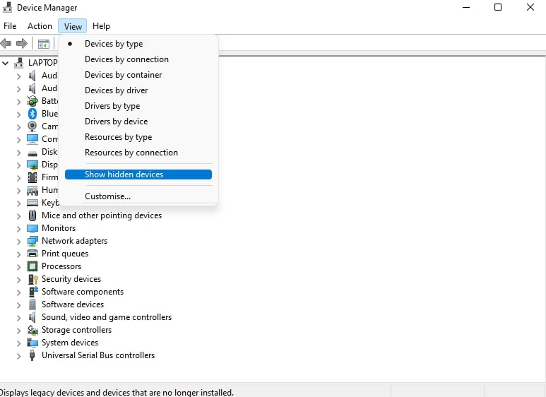
With this newfound knowledge, I plugged in both devices and noticed the demo board was intermittent in showing up, while my board showed up consistently :)
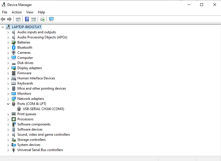
In short:
- install drivers
- show hidden devices in COM port under Device Manager
Test
After searching around the internet, I stumbled upon something called a loopback test for FTDI devices, and instantly remembered what our instructor, Steven, showed us some time ago. To do this test, all we need to do is to add a jumper across the TX and RX pins of the FTDI pinouts (or in my case I couldn’t find one so I used some spare pin headers to beidge the TX-RX pins).
Here is the result, the test was successful!
However, I was quite stumped as in order to test whether the UPDI adapter would be working, I was thinking that I need to test it with a AT-series-1 or -2 board, which I did not have any at hand.
Luckily, Mr Rodney was in the Fablab today, so I asked him about how should I verify that it is working. The suggestion was simple, do a connectivity test from the FTDI board to the UPDI board as the traces are visible, we have the board schematic, and the test is doable due the board being relatively simple and straightforward. I checked the schematic, and all the corresponding readins check out :)
In the following weeks, I will be sure to test the FTDI-to-UPDI adapter with a proper micro-controller, but for now I believe this should be sufficient.
Design Files
This week i did not design any files, as our instructor Steven has made very good boards that are not only easy to manufacture, but also easy to understand what needs to be done. The png file will be linked to as it is potentiall large.
- trace test: trace outline
- FTDI (CH330) files: schematic trace outline
- FTDI-to-UPDI adapter files: schematic trace outline
Last week leftover tasks
I explored Living Hinges, it was a ton of fun. I would love to study the APIs a bit more in depth, and possibly do more with what Cadquery can do :)