7. Electronics design
Editor’s note 2023
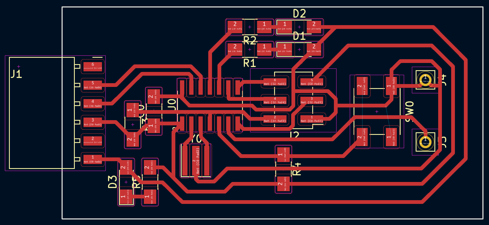
Some of this assignment was done during the old assignment 5 when we went straight to electronics production to make ISP. So the KiCAD printscreens are mostly about making the TinyISP.
Group Assignment - Test/Diagnostics Equipment
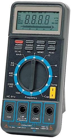
Multimeter
As the name suggests, Multimeters are used to measure a bunch of different stuff, most comonly voltage, current, resistance, capacitance and continuity. My old Protek D981 can also test diodes, check frequencies and even has a temperature probe attachment.
Measuring Voltage is easy, just touch the probes in series:
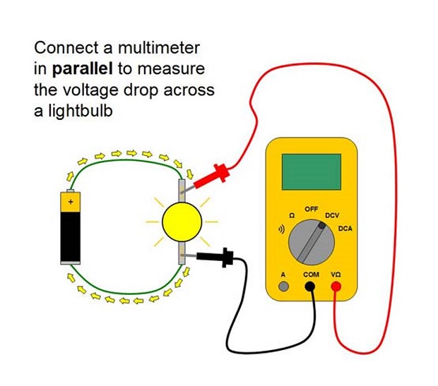
Here’s me using it to test the I2C pull-up resistors on my final project’s motherboard:
As you can see one of them is working especially bad. Could be the soldering, bad/burnt resistor… It needed my attention.
If you want to read more about using a Multimeter here’s a nice tutorial.
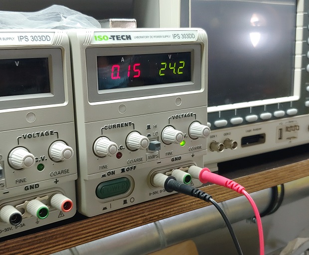
Lab Power Supply
To power our devices during development we need a stable DC voltage and the easiest ways are either directly from a battery or a more versatile bench Lab Power Supply.
These come in different shapes and sizes. When buying one they’re usually listed by Max Voltage, Max Current and number of channels. Plus more or less extra features.
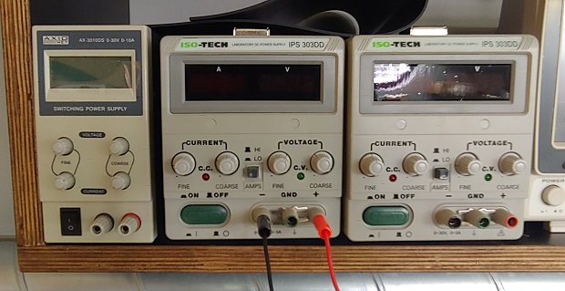
They generally have a pair of knobs to quickly change Voltage and Current limits.
I’ve seen smart power supplies that can emulate dirty power patterns to help debug possible points of failure in circuits. For example instead of supplying a very constant 5 Volts it can generate specific and periodic noise signatures to influence and possibly trigger problems beyond what decoupling capacitors can handle.
Oscilloscope
Can’t fault the wikipedia’s description:
An oscilloscope is a type of electronic test instrument that graphically displays varying voltages of one or more signals as a function of time. The main purpose is capture information on electrical signals for debugging, analysis, or characterization. The displayed waveform can then be analyzed for properties such as amplitude, frequency, rise time, time interval, distortion, and others.
Some can also act as Logic Analyzers.
I intended to use the Oscilloscope to help me debug some instability on the I2C bus on my Final Project. See if there was any inintended noise flying around the power, SDA or SCL lines.
Here are 2 videos I watched to make sure I kinda knew what I was doing.
How to Use an Oscilloscope - Direct link
Finally have an excuse to link an ElectroBOOM video! Yey What’s an Oscilloscope - Direct link
The demo signals are easy to find.
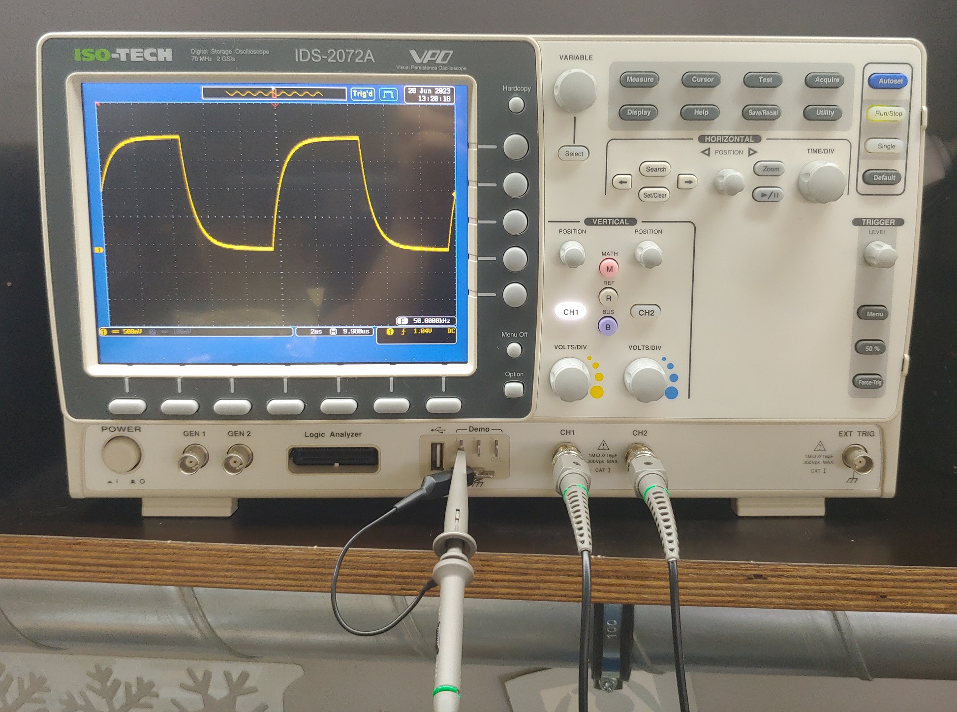
But I couldn’t figure out how to check for noise. I can think of 2 reasons:
-
and biggest of all I just don’t really have a base line for what a noisy signal would be if I saw one lol. Everything’s noisy if you look close enough.
-
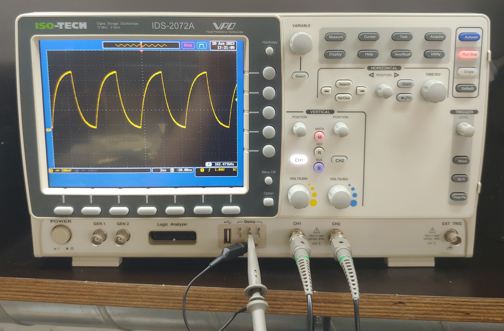
I wasn’t able to determine how to zoom in below a certain scale. It would always default to mV values far from the actual signal and too far off that it wouldn’t let me adjust it further. ChatGPT said it probably had to do with the way the trigger function works but even after some tinkering it didn’t make a difference.
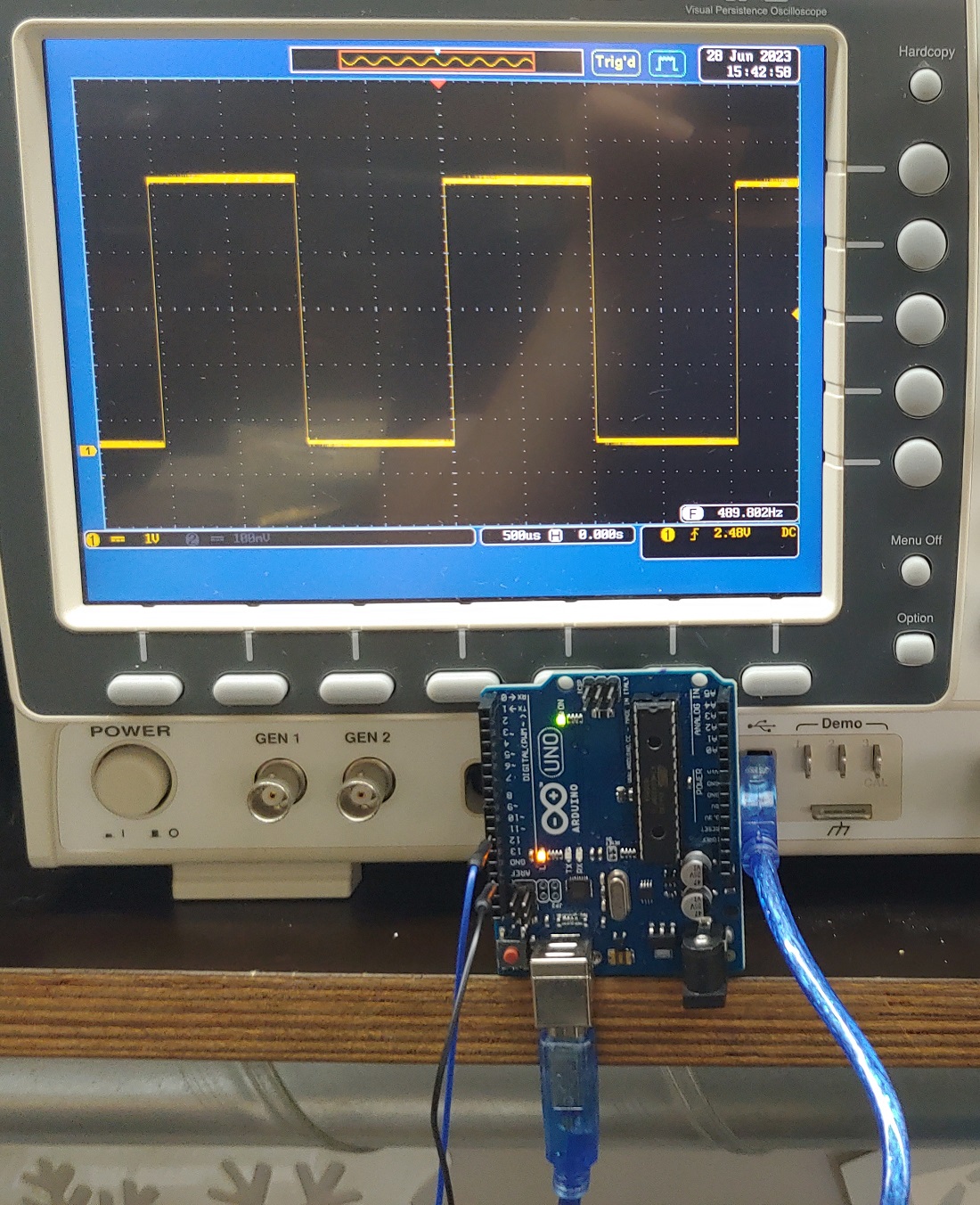
Since I still had to measure a micro-controller working I remembered AnalogWrite() was a fun option. AnalogWrite() isn’t actually analog, it’s just PWM that has to be smoothed through a capacitor and resistor to get a stable voltage. I quickly wrote a sketch with one of the Arduino Uno’s PWM pins in mind (Pin 10):
void setup() {
  pinMode(10, OUTPUT); // pinMode() might be optional with analogWrite()? Didn't test.
}

void loop() {
  analogWrite(10,127); // pin, duty range 0-255 , 490hz - pins 5 and 6 run at 980 Hz on the Uno
}
After uploading it I connected the Uno to the Oscilloscope to find the expected 50% PWM signal at 489.8Hz.
Individual Assignment - Design a PCB.
Before you start you should go check Aalto Fablab Youtube channel. They have a bunch of really nice videos on diferent topics that cover plenty of assigments.
Including this introduction by Krisjanis Rijnieks. Direct Link
If you can get your hands on it Neil also recomended a book called The Art of Electronics by Paul Horowitz and Winfield Hill.
Setup EDA - KiCAD
From what I found KiCAD seems like the most used EDA program in FabAcademy.
![]()
My instructor actually prefers EasyEDA since it already has components integrated but I don’t like to rely on always-online web-apps…
Altium seems to be the Solidworks/Catia of electronics design. Very expensive but a lot of expert functionality, including advanced simulations.
Wikipedia has a nice EDA comparison page.
KiCAD Libraries
While KiCAD has some included components and you can make your own it’s easier to import big bundles called libraries.
There’s a small oficial library list on the KiCAD website.

Keep in mind that while the Digikey Library is quite big, it’s unmaintained now. There are a lot of symbols and footprints that aren’t linked so it might make searching for components harder instead of easier. Until you’re comfortable editing footprints and pre-defined relationships between symbols and footprints I’d recomend you avoid it.
Thankfully there’s a Fablab Library too. Just happens to be maintained by Krisjanis. He has a todo list if you want to help out. Last I spoke to him he’ll take all the help he can get with 3d modeling components. Doesn’t have to be fancy, the simpler and smaller the files the better. Modular files with parametric spreadsheets go a long way for components with a lot of variants like pin number in SOIC packages, etc.
Follow these instructions to install the library:
- Make sure you have at least KiCad 7 or greater installed.

1 Clone or download this repository. You may rename the directory to fab.
2 Store it in a safe place such as ~/kicad/libraries or C:/kicad/libraries.
3 Run KiCad or open a KiCad .pro file.
4 Go to "Preferences / Manage Symbol Libraries" and add fab.kicad_sym as symbol library.
5 Go to "Preferences / Manage Footprint Libraries" and add fab.pretty as footprint library.
I can recommend looking at component providers like SnapEDA and Ultra Librarian. Just search for a component you need and download it. Sometimes they might not have the specific component you want, but if you look for a similar model it might have the same pinout and footprint.
Editor’s note 2023
This part is a bit of a mess. While the process is the same the contents of my printscreens might not match this assignment because they were taken while I was documenting making an ISP with a tiny45. Some components might seem out of place but the buttons I pressed to make something happen are the same.
For this assignment it’s advisable you start with one of Neil’s Hello Boards.
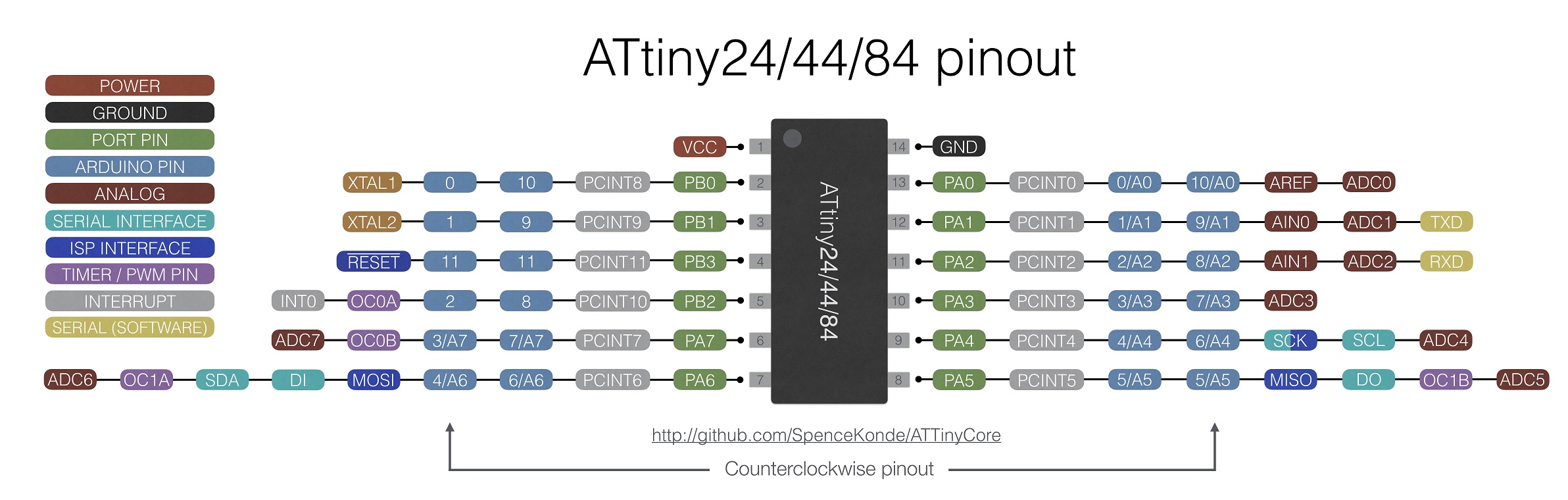
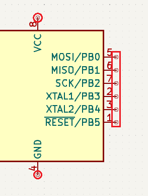
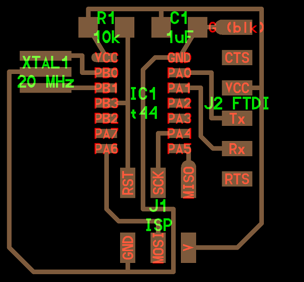
I wanted to connect a few things to the micro-controller so I went for a Tiny44 and it’s 4 GPIO pins that didn’t overlap with the SPI interface. You can re-use them but there are things you need to be aware that I knew I didn’t know and didn’t have time to learn.

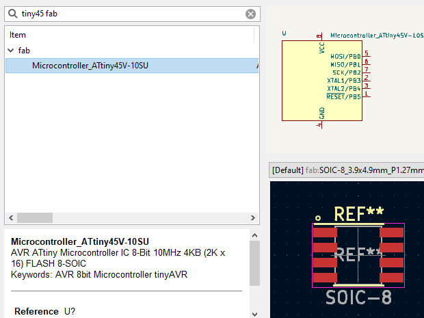
The 1st thing to do when designing a new board is looking at datasheets and pinouts.
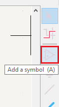
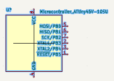
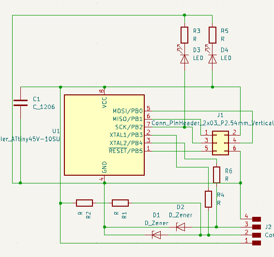
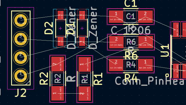
With that in mind we start by adding a symbol in the Schematics Editor.
It doesn’t matter which ones you add first or the order you connect things.
Place it anywhere, you can move them later if needed.
I’m a fan of just throwing everything in there so I don’t forget about anything.
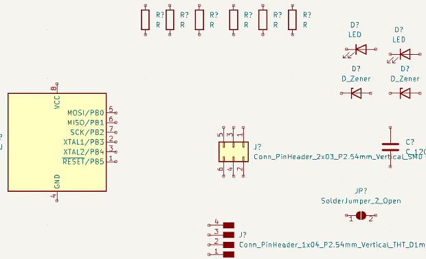
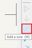
Time to use Wires to link components.
Make sure you pay attention to the pins. Connecting things to the wrong pin can be catastrophic.
When you have a lot of components using just wires can be a bit messy. There are also tags you can use. It’s how you connect things between pages.
Click on the Update PCB button.
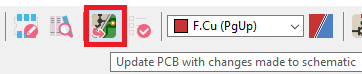
Let it do it’s thing.
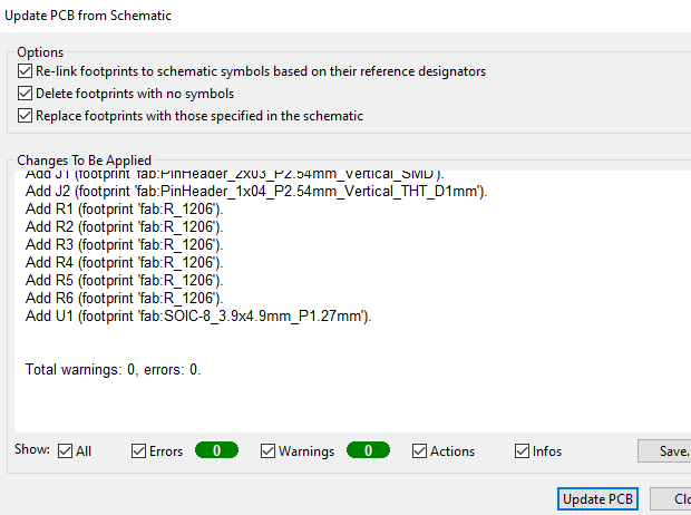
Just say Yes until you know what you’re doing.
That should open the PCB Editor automatically, but just in case remember there’s a button like for the Schematics Editor.
On the 1st time opening all components will be bundled and floating with the mouse pointer. Click anywhere you want.
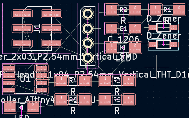
I’d recomend hiding some layers to clear the screen of unecessary clutter.
In this case I was copying directly a screen grab of the ISP.
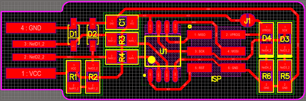
But laying out everything as the example Hello Board is a good way to guarantee all the bases are covered. You can edit things later.
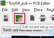
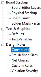
Design Rules
Before starting to lay traces it’s important to define the Design Rules so that KiCAD knows how to relate the physical aspects of the PCB.
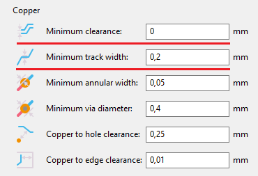
Design Rules mostly depend on what you can manufacture, by milling or what the Board House you’re hiring to make your pcb’s can do. There are also constraints related to the components you’ll be using. If you need a component that has tiny pins, then if you can’t make the pads for them you either change component or the machine/tooling/Board House.
The line test Neil has is a good start in a Fab Lab. My instructor didn’t know how to turn the png to g-code on Mods so I just ended up using the settings he recomended at the time.
Navigate to Constraints.
Track Clearance and Width are probably the most important for now. After some practice you get used to pick your own. I usually settle around 0.4 for both. These might not be the final measurements if you’re machining it but that’s for another assignment.
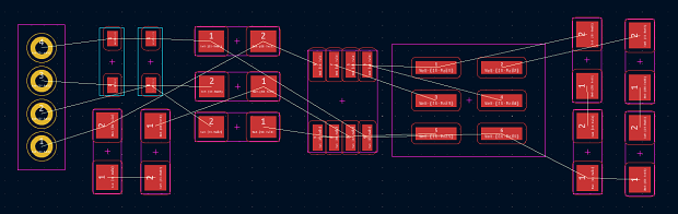
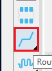
Click the Route button. Keyboard shortcut is X, comes in handy.
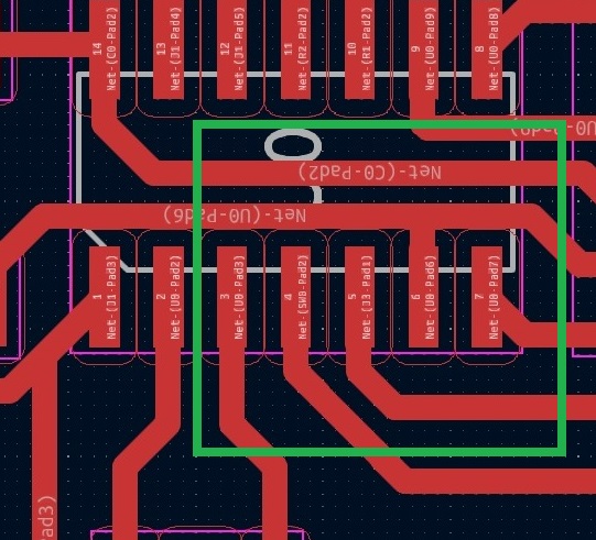
Clicking on a pad will highlight other pads in the same NET groupnig.
Connect all.
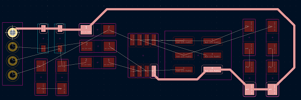
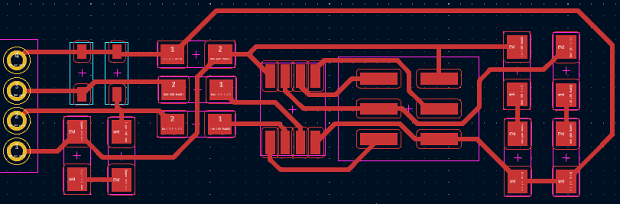
In this I was copying the example and while all routing tutorials feel like the Draw the rest of the Owl meme it really is just about getting some practice…
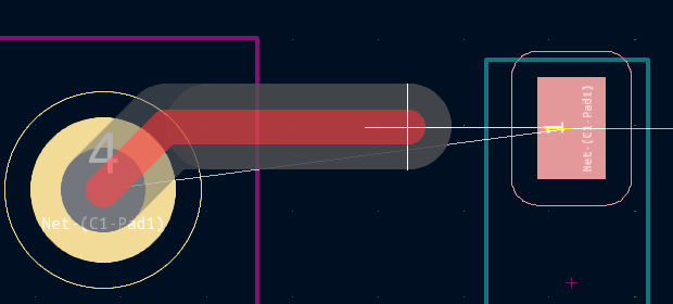
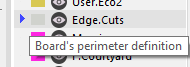
Now the new board needs a perimeter. Select the special layer.
There are a few options on how to draw the limits. You can even import an svg if you want.

Draw a shape around the board.
Editor’s note 2023 - Fabrication
It’s optional now but since I also documented this part…
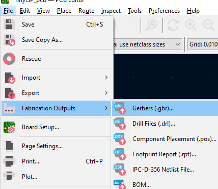
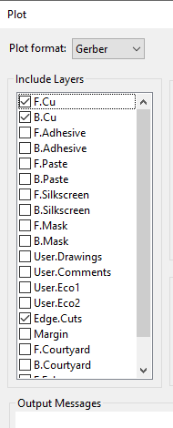
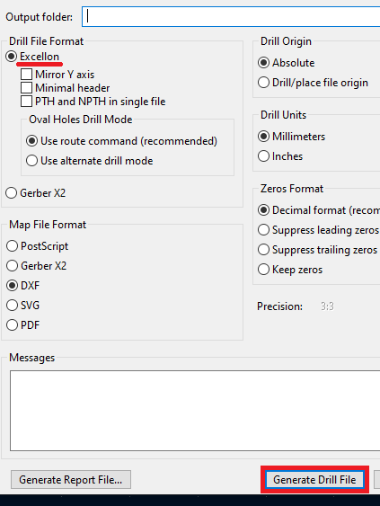
For milling you’ll need the the Front Copper and Outline .gbr files.
You can leave the directory unchanged if you want. I like to add a new folder to keep everything tidy.

Click away.
And hit Plot!
We also need the .drl file with the hole information for drilling. Excellon seems like the most compatible encoding.
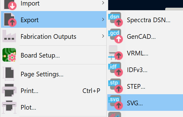
Beyond the .gbr files some tools also accept image files such as .png and .svg.
Just pick them in the export menu.
Select the layers you want to export and click the export button.
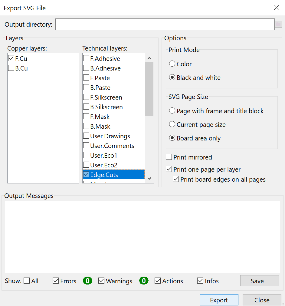
By default they’ll go to the same folder as the KiCAD project.
It’ll generate something of the sort: Copper - Outline
Editor’s Note 2023 - Input Assignment
Towards the end of Input Assignment there’s also some more Electronics Design topics about keeping noise and capacitance in check. I had a lot of problems with making my final project’s motherboard and with the ESP32-C3 module I use in 2023. Ended up documenting a lot as I tried to find the problems and solutions. My main goal was to make my I2C BUS more reliable and found a lot of relevant topics even if they’re mostly above our pay-grade.
Debugging - Hardware Revisions
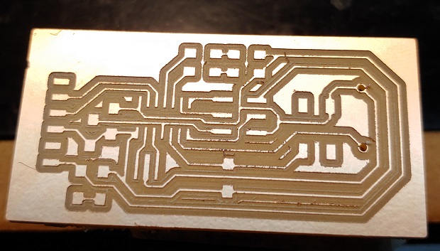
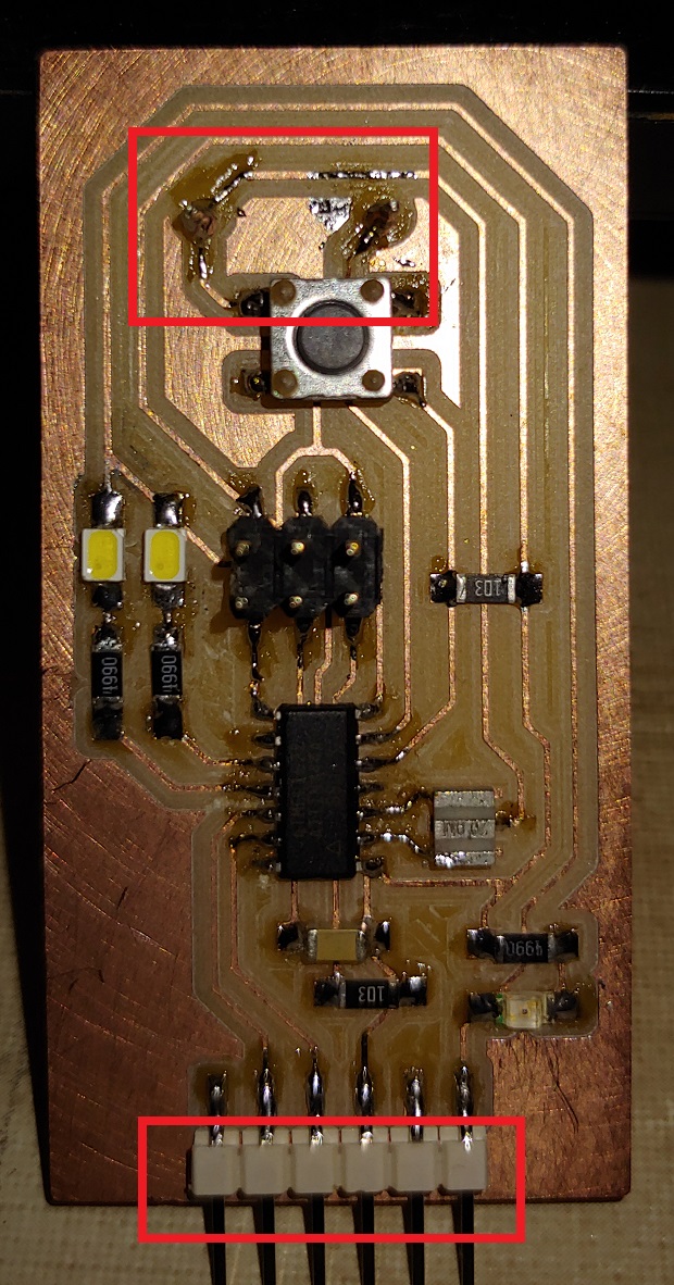
I did end up milling my T44 board but it didn’t work, twice.
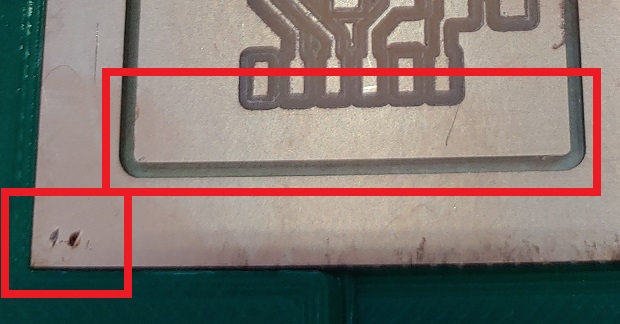
This is my 1st board with 3 problems highlighted.
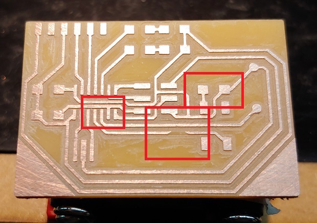
I wanted to clear the copper but slipped and shaved off a bit too much.
I thought I could cover the whole copper strip in solder to hide it, but as soon as I melted one side the other came flying off from the heat transfer through the copper and I never managed to get it looking as pretty as the 1st picture…
Stuffed all components.
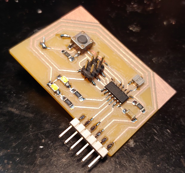
This is what it looked like by the end as my instructor didn’t notice my resistor wasn’t connected right and…
Originally I wanted the button working, the LEDs to count to 3 in binary and the buzzer beeping along. Turns out inputs need a very specific use of resistances called Pull up/down Resistors. Sometimes they can have them included.
The basics are that pins left on their own are in a state called floating. They are neither High nor Low. The resistors pull the voltage on the input circuit either to High or Low. Hence the Up and Down.
This is the best explanation I found on the topic.
I knew I needed a resistance but I didn’t understand why and it wasn’t connected properly making the LED turn on and off incoherently.
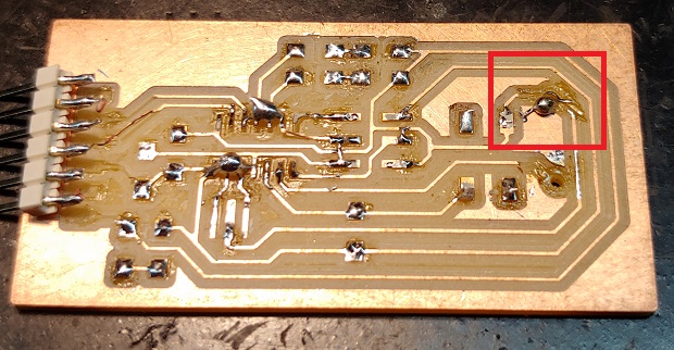
Also, remember the original board? Notice anything different on my pins?
Well turns out pin 11, the Reset pin, is quite important. Ya can’t just move any pins around, pins’ functions are detailed in Datasheets and on Pinout tables. Sometimes Datasheets will go on about “Strapping pins” these pins have special functions and need to be wired in specific ways.
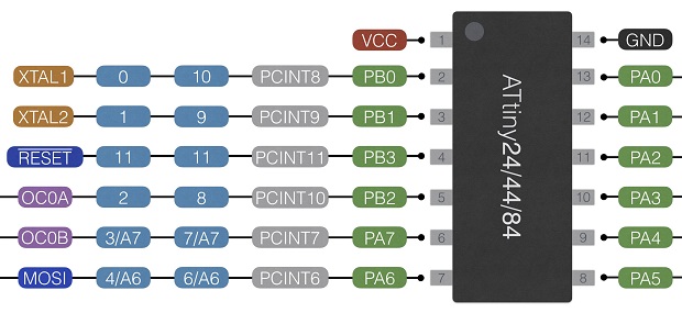
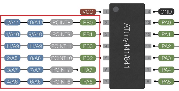
Speaking of pinouts, if you find this and are having trouble getting chips called ATTiny441 to work try the alternate Arduino pin naming scheme. By default they seemed to use the pins closer to PCINTx instead of the ones further away. The 441 is similar to the 44 but not identical.
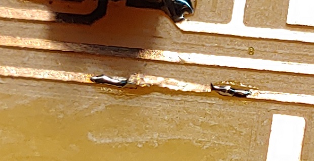
My 2nd try with the reset pin and pull-up resistor in place. Traces ended up a bit thin because of the v-bit going a bit too deep. But that’s a story for Electronics Production.
To start I stabbed the plate, setting the 0 on the Carvey has a lot of steps and I broke too many bits because I forgot 1 or 2… Didn’t break the machine so that’s an absolute win on my book.
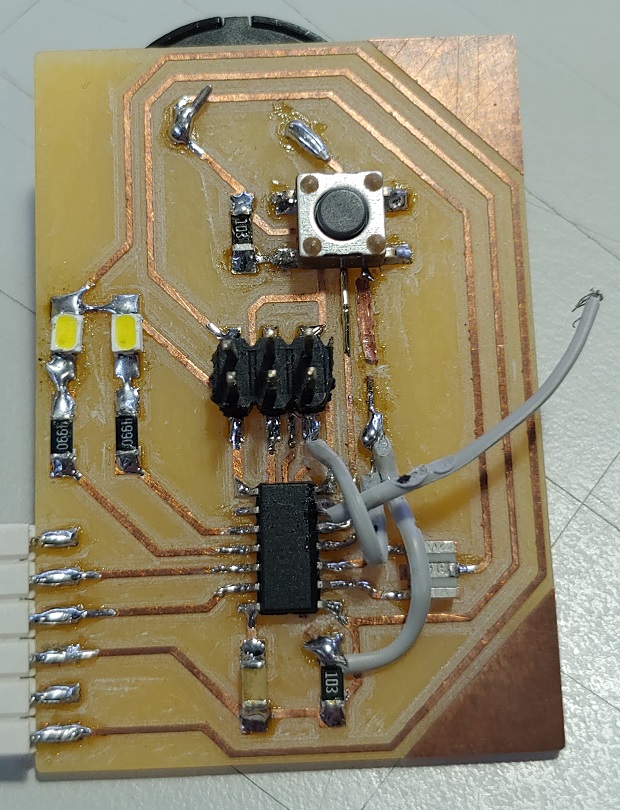
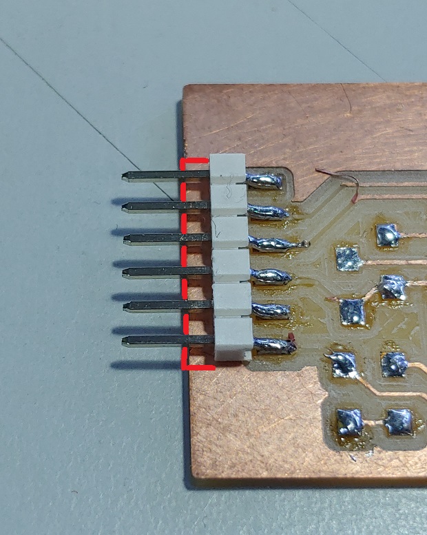
The biggest problem is the connector margin. It’s too big and it’ll come back to haunt me in a bit. Problem compounded by the thin traces. The pads on the 1mm through-hole are also too small so they failed quickly. Once I figured out how to edit footprints I started making them bigger.
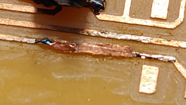
I didn’t solder the male FTDI connector pointing up so I always had to force it up so the cable connector wouldn’t get stuck on the side of the board. Eventually the traces failed and the whole thing came off.
I used the oportunity to try and de-solder everything with the soldering iron, I became much more careful with putting side mounting connectors like this. Also gluing all connectors now seems like a great idea. In this case I should have soldered the contacts at an angle.
With everything I learned I re-did everything a 3rd time and gave up on programing the button and buzzer for now as I used up all my time. I only needed a blink to begin with but I needed to learn about all this anyway so might as well be now.
Editor’s note 2023 - Programming it
Last year this assignment came before the Embedded Programming assignment so I only need a simple Blink program to show that the board and MCU were working.
Now I moved that into Embedded Programming Week if you want to read a bit more.
After everything I got it blinking and was very happy that it was working!

Bonus Round
This was the program I wrote for this board for the Embedded Programing Assignment. Binary button press counter.
Files
In case you want one: