Autodesk Eagle
Schematic
I have never had to design any electronics. It means this week I was carefully trying to follow Antti's instructions. He suggested us to use Autodesk Eagle, and introduced step-by-step instructions how to work with the software.
At first we installed Autodesk Eagle and fab.lbr library for Eagle, which contains all the components used in Fablab Academy.
Having the scheme of
echo hello-world board as an example we started the design.
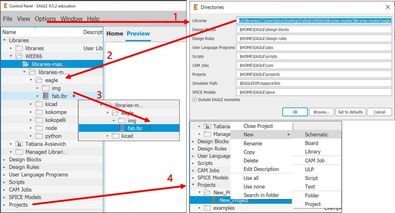
- In the Eagle Control panel go Options> Directories and indicate the path to the Eagle library. Now libraries can be seen in a vertical list on the left panel. fab.lbr should be enabled by clicking on it, grey dot will change to green, denoting the activation.
- In the Projects go to projects folder and create the New Project (also should be activated with a green dot appearing). From the New Project> New> Schematic.
Fig 1. Starting new project in Autodesk Eagle
- We started the
shematic.sch drawing.
Fig 2. Starting Schematic in Autodesk Eagle.
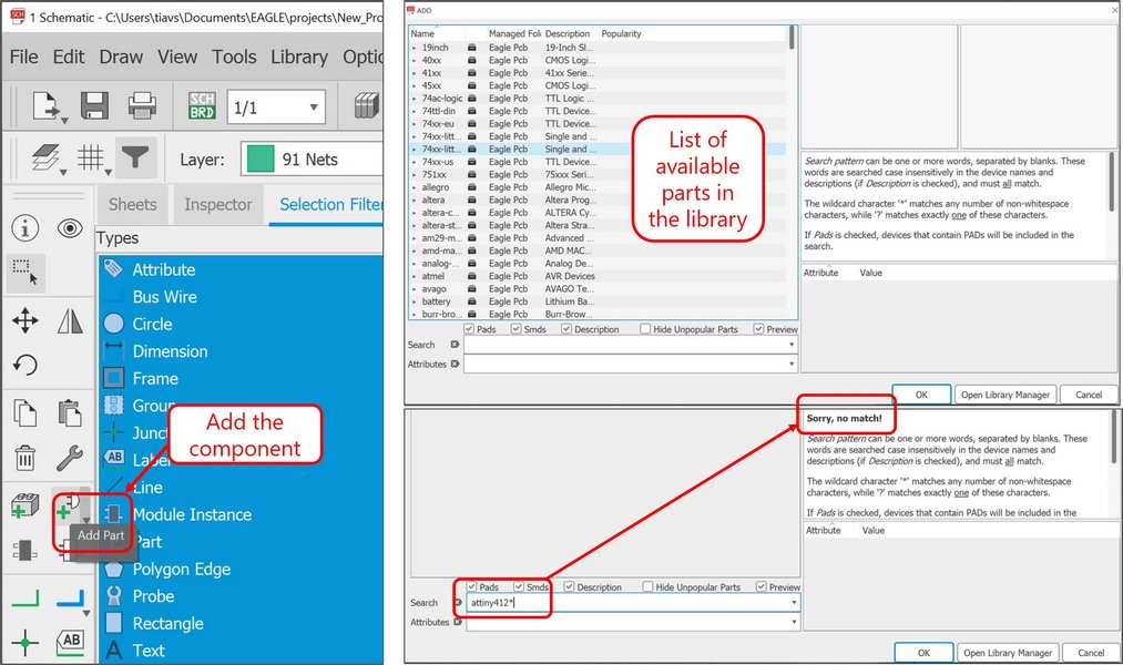
- Add part tool opens up the list of the components from the library. When we tried to search for ATtiny
part, we got no results on it in the existing library.
- That means we have to find the part footprint somewhere else. We found ATTINY 412 on SnapEDA. The symbol is missing, but there is a possibility to build it with an option Build Symbol.
Fig 3. Starting Schematic in Autodesk Eagle.
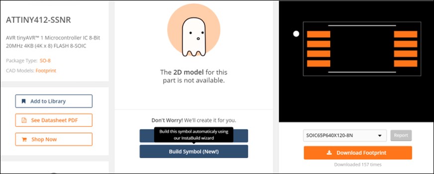
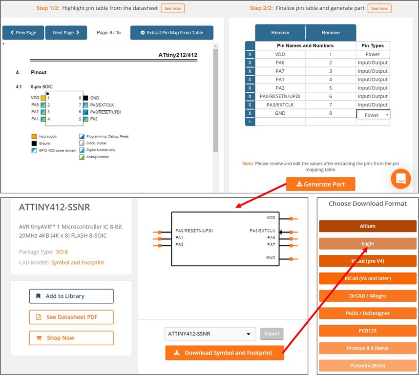
- When we signed in on SnapEDA, we could start building the part. Having a Pinout sketch (page 8of the datasheet) on the left we added Pin names and numbers in the table on the left.
Fig 4. Building the ATTINY 412 part on SnapEDA.
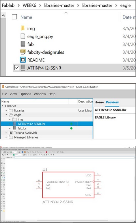
- The new part should be moved in Eagle library directory to be added to the library.
Fig 5. Importing the part in to Autodesk Eagle.
- This was a nice experience, cause we realized, that ATTINY412-SSNR , is not the right type we need. Before we managed to generate another part for the type right type ATTINY412-SSF, Antti has already sent the right footprint to us. The part can be added to the library, and then it appears among the available parts.
Fig 6. Importing the part in to Autodesk Eagle.
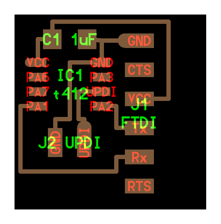
- To build the scheme of the board we used the following tools:
Add part - add part from the library (select VALUE)
Move and rotate - move parts and change the part's position
Net - toll to connect the parts
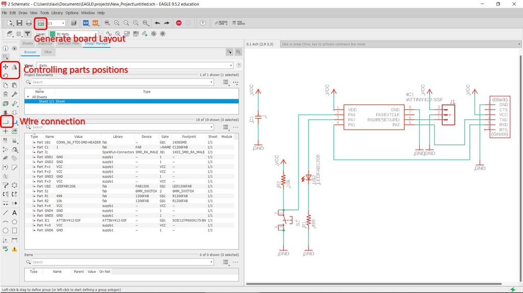
Fig 7. Finished schematic of the board with a list of used parts.
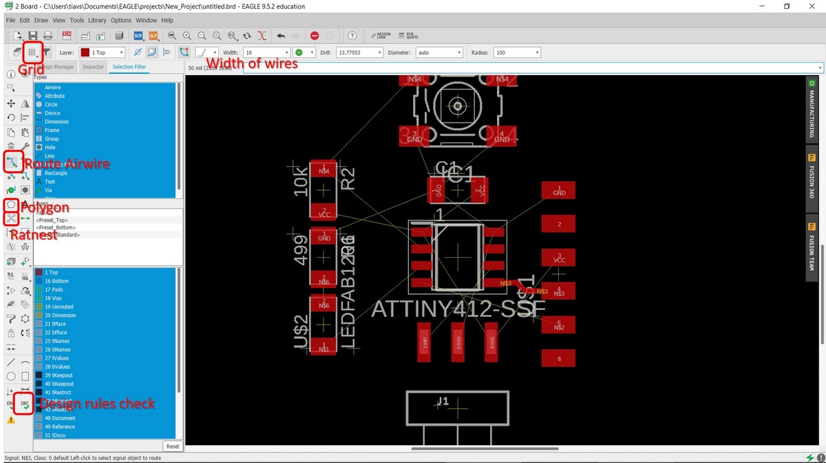
Layout
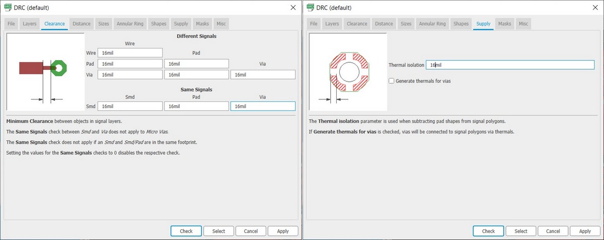
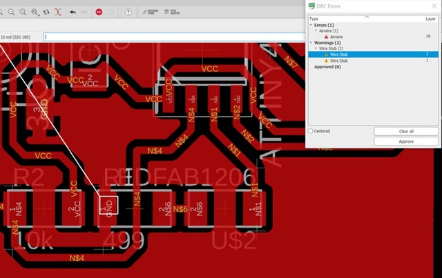
- To proceed with a board Layout editor click on Cenerate/Switch to board icon. Things appeared quite messy, and we started arranging them with Move, rotate tools and drawing airwires with Route Airwire tool. We set a width of a wire to 16 mil. Grid tool allows to set the distance between the paths, default value of 50 mil can be changed by holding
Alt. Be sure to do this being on the Top layer, which is marked with red color.
Fig 8. Layout generated from the Schematic.
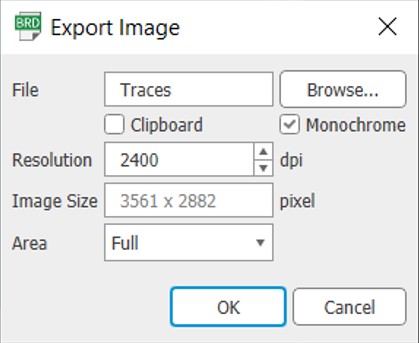
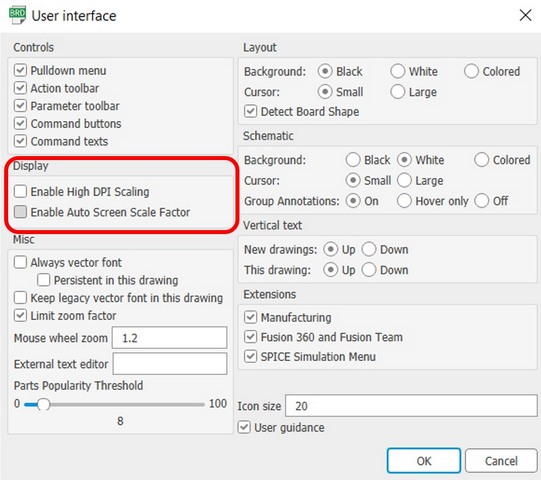
After exporting the PNG files we realized, that size of the image has been changed to a significantly bigger dimensions, despite that all the size related settings were right in the Eagle. Eventually we realized that Display in the User preferences should be unchecked for an adequate exporting.
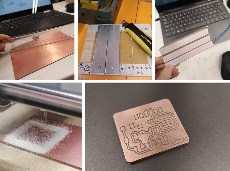
PCB Milling
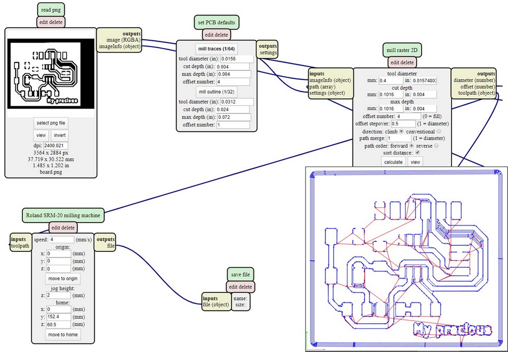
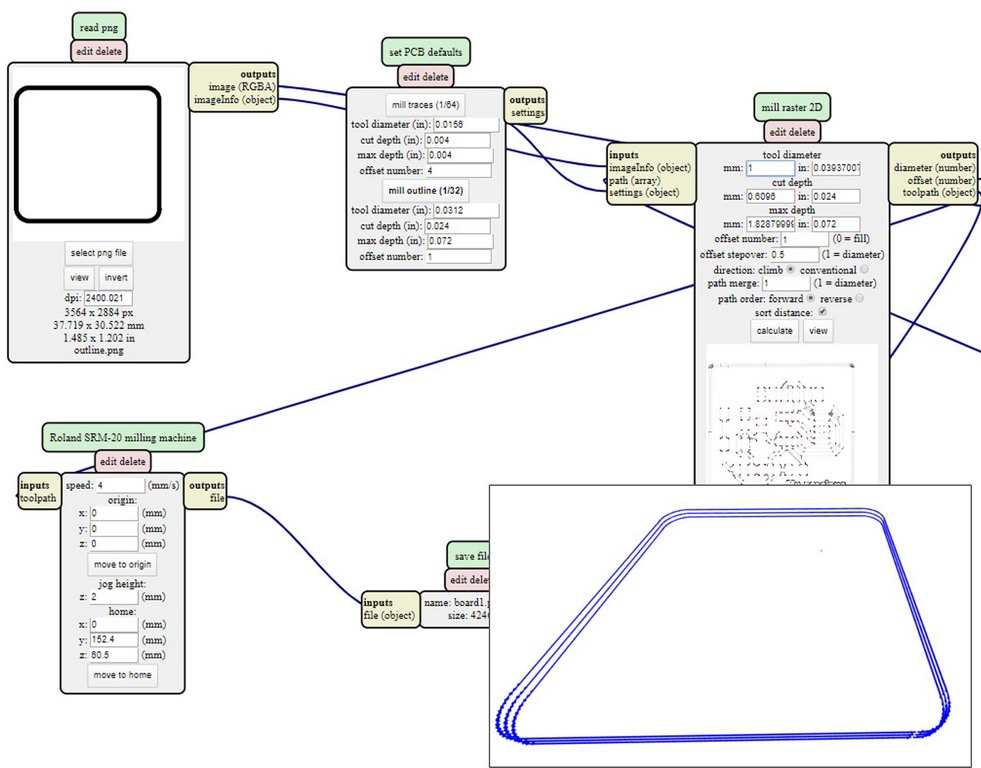
I used Mods to generate the .rml files for milling. The used settings are on the images below:
Fig 12. Generating .rml files for Traces and Outline.
Fig 13. Basic steps for milling prepartion and final result: checking the flatness of the FR-1-PCB blank, cutting the piece of the blank, fixing with a double-sided tape, milling and removing the superficial layer.
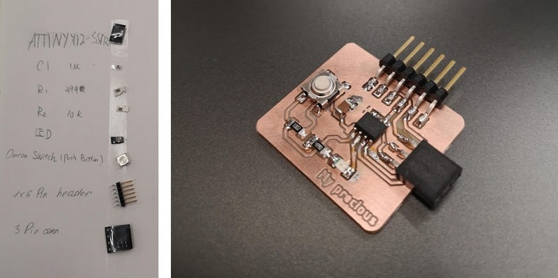
Soldering
Fig 14. Soldered components on the board.
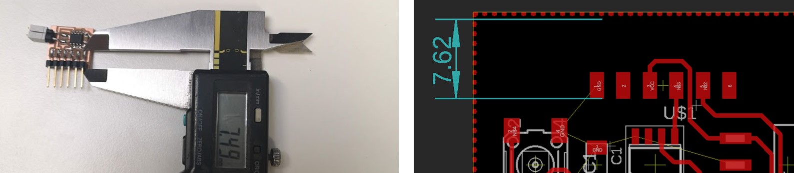
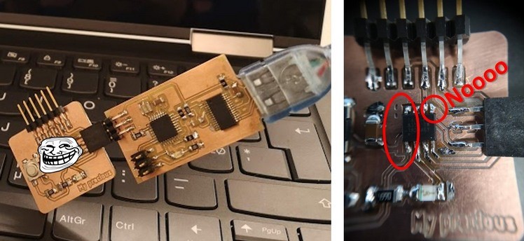
I used the UPDI programmator made during Week 4. Electronics Production. My soldering looked absolutly fine, however the programming would fail every time.
We started looking closer on the board to find a possibile mastake, but everything looked good. Until Antti's professional eye found the problem - ATtiny microchip was shifted exactly by 1 pin to the ground. My GND was milled in a way that it looked like a trace. I couldn't resist and soldered the pin to the GND.
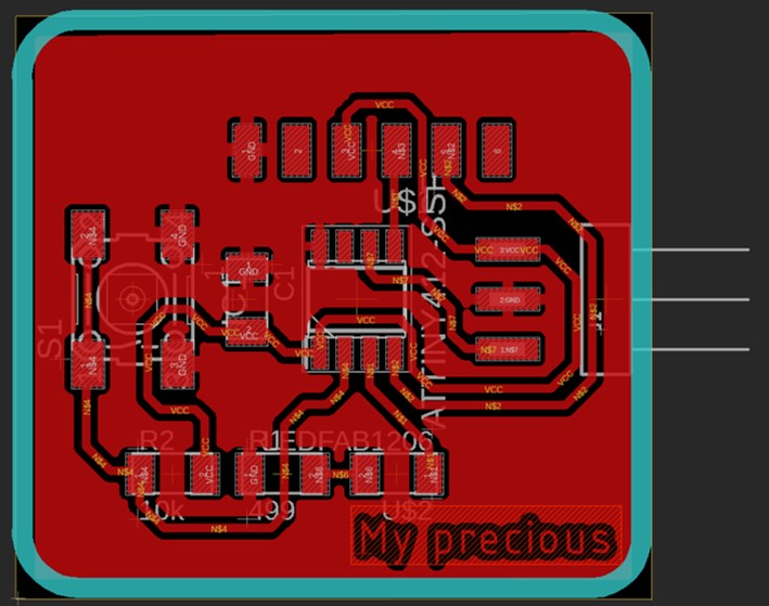
Fig 15. Trying to program the board. Even the "precious" board can have a flaw.
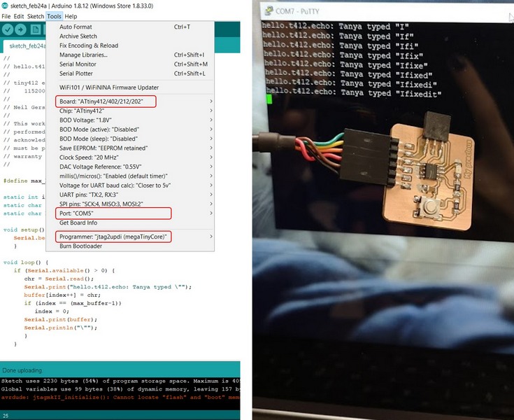
Weaponed with a hot gun I fixed friday evening mistake the chip's position. Programming went successful.
Fig 16. Programming the echo board with Arduino IDE. hello.t412.echo.ino program burned on ATtiny returns an echo typed in Putty command prompt.
FILES:
Reflection
This week went fine as I was mostly just following the instructions. I'm trying my best to understand the electronics, and hopefully it will become more clear:)
