Milling PCB with Roland SRM-20
- FR-1-PCB blank. The cutting was done on the FR-1-PCB blank. At first, blank should be as even as possible, it can be check with a simple ruler. If there is gap between the ruler and the blank, gently bend the plate till it is evenly flat.
- Blank fixing. The material should be fixed reliably on the stage inside the machine. For that the simple doudble-side tape stripes were used. We decided to use the big piece of material, however it was not the best idea, as it was harder to achieve even flatness on the whole piece.
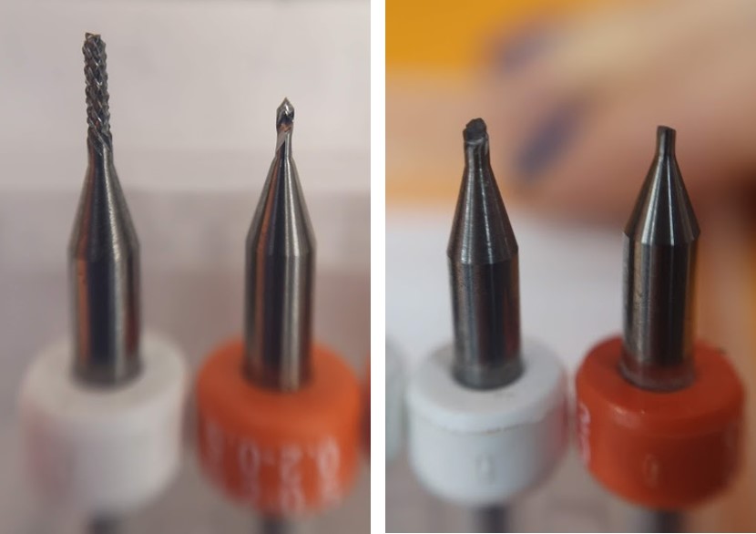
- Installation of the milling bits. For Traces and Calibration of PCB I used V shape 0.2-0.5 mm milling bit, while to cut the Outline flat 1 mm bit was used. To install the bit into the machine, it should be hold with fingers and placed to the collet, while holding it in the place, tight it with a hex key carefully (the excess of the pressure may cause the break). Milling bits require careful handling as they break easily if dropped.
Fig 5. Milling bits flat 1 mm white and V shape 0.2-0.5 mm orange, and just to compare, some examples of broken bits.
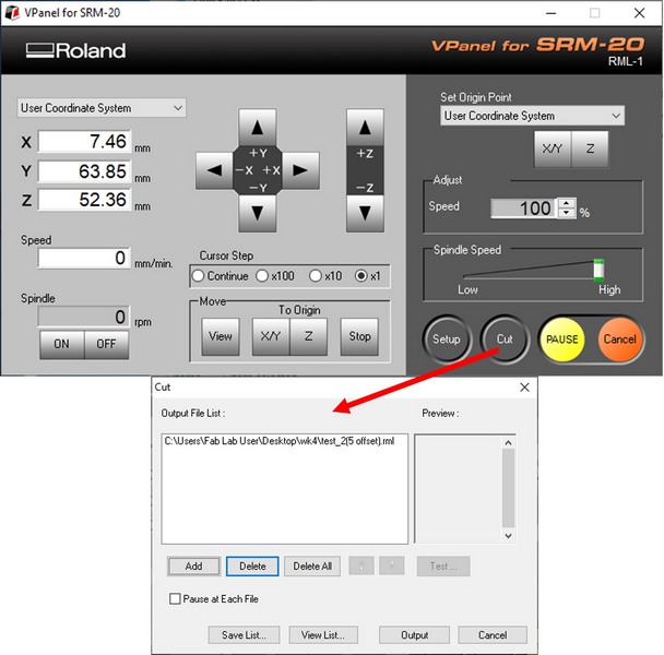
- Vpanel for SRM-20. To start the software the button on the right top of the machine. The detailes of use are explained in the Group assignment page.
- Set the Origin for X, Y and Z. Cursor steps are optional: continious mode or jogs by 1 mm, 0.1 mm or 0.01 mm. Locate the milling bit on the laft bottom corner of the blank (default origin). Set the origin for XY position.
- After X and Y positions are set, move slowly along the Z position untill about 1 mm to the surface of the blank. Then untight the collet and let the milling bit touching the surface and fasten it again. Set the origin point to Z. It is better to start milling slightly highler to ensure that surface is evenly flat, and in case it is not, try to fix it the blank bending or adding the tape underneath.
- Press the Cut button and add the .rml file.
- Press the Output
- The procces can be paused with PAUSE button and checked for the milling quality with a View button
.
Fig 6. Vpanel for SRM-20
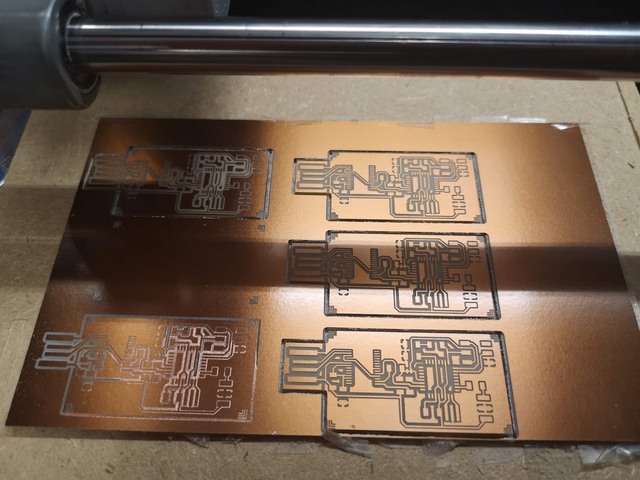
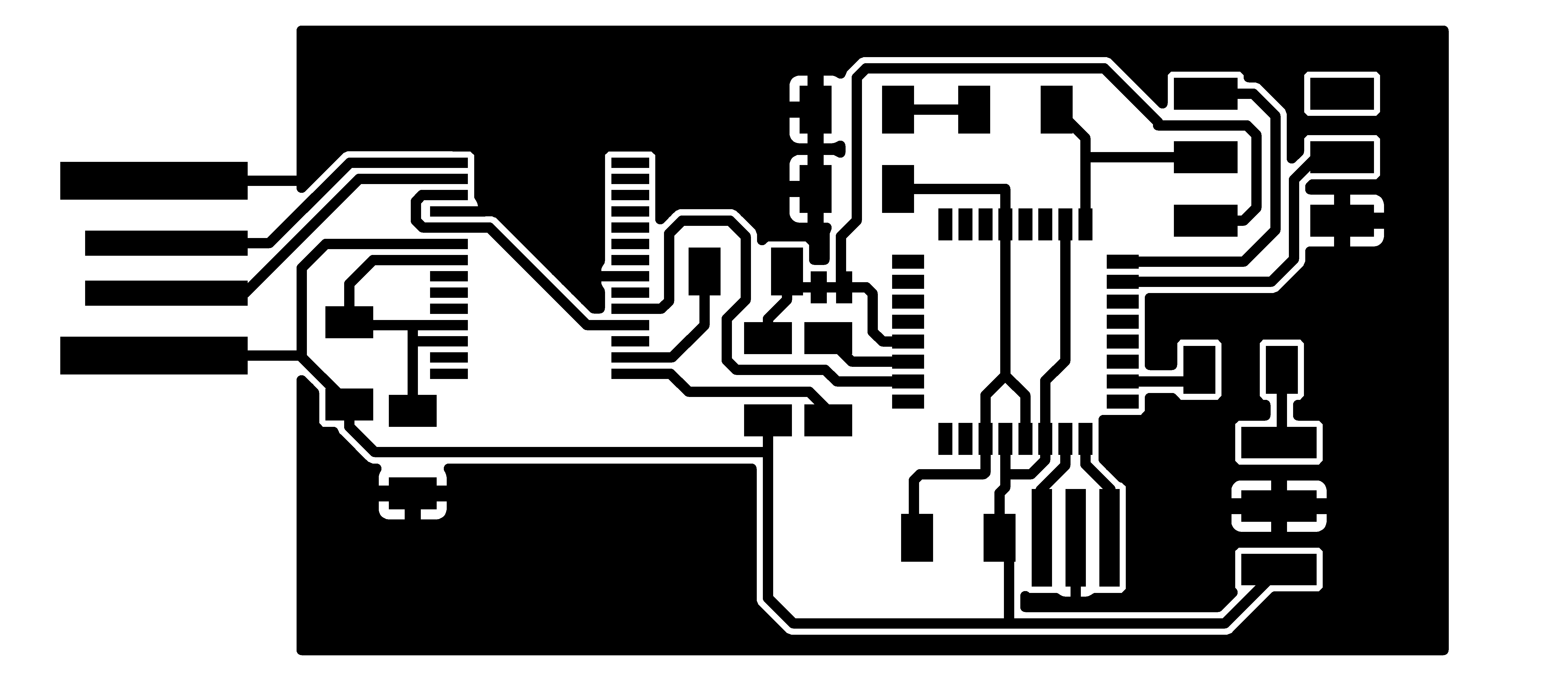
We cut few boards on a single blank. At first the Calibration and PCB traces were milled with 0.2-0.5 mm bit, and after changing the bit, the Outline was milled with 1 mm bit, as we remembered the Origin position for each board.
It can be seen, that the first bottom board was not milled evenly - bottom right part traces are not deep enough. Before proceeding to other traces milling, the blank was bend again. After finishing the milling boards were removed gently from the stage using the spatula.
Fig 7. Results of milling with SRM-20
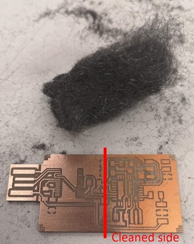
At this stage the board have to be cleaned from the superficial layer of the material. Gently scrubbing PCB surface with a metal spounge it was cleaned (сolor has become lighter). At the last stage front contacts for USB port were covered with a thin homogeneous layer of tin to protect copper from the oxidation.
Fig 8. Results of milling with SRM-20
Soldering components - PCB assembling
Soldering part took most of the time due to the luck of experince and the fear to screwed up. To be able to solder for a significant amount of time I made the place comfortable. Things to be used:
- Holder to fix the PCB
- Soldering iron at the temperature 350 Celcius
- Solder - tin metal
- Fume extractor, cause harmful smoke is produced during the soldering
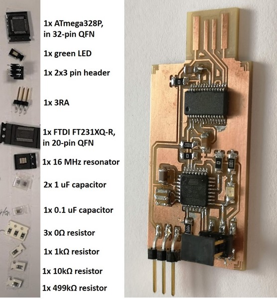
And of course the list of COMPONENTS to be soldered:
Fig 9. Components for soldering and final PCB
Programming the AVR microcontroller of the PCB
- When the PCB was ready, I checked it visually under the microscope and with a multimeter, for possible soldering defects (short circuit). To make the board fit properly into the USB port few layers of the sticky tape were applied (3.21 mm).
- PCB board was connected to USB port to be programmed. USBtinyISP was used to programm the microcontroller with a new firmware. The device can be seen as a new device in a Device Manager. In the Ardiuno Software Tools choose:
- Board: "Arduino Nano"
- Processor: "ATmega328P (Old Bootloader")
- Port: COM"the port device connected to"
- Programmer: "USBtinyISP"
- Tools> Burn Bootloader
- The simple programm was ran succcefully making the LED blinking faster. Now PCB is a an ATmega328P-based Arduino board.
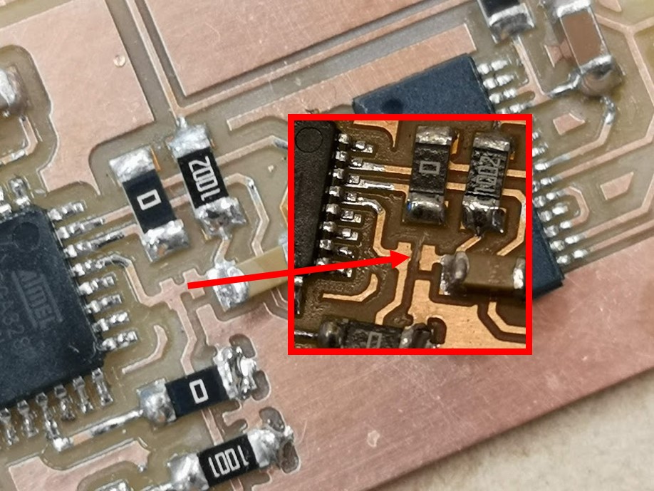
- Before proveeding further, the path connecting microcontroller and FTDI has been cut. It can be restored in case if some changes needed to be introduced.
Fig 10. Components for soldering and final PCB
UPDI programmer
UPDI programmer was made by installing ElTangas's jtag2updi program on my ATmega328P-based Arduino board following
next steps:
- Download jtag2updi and extract files to one folder (important: all the files should be in the same directory with
jtag2updi.ino sketch file.
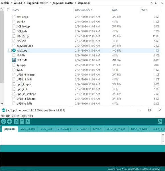
- Open
jtag2updi.ino sketch in Arduino environment. Empty .ino file needed for compiling, while the code is contained in all the other files.
Fig 11. Opening the sketch jtag2updi.ino
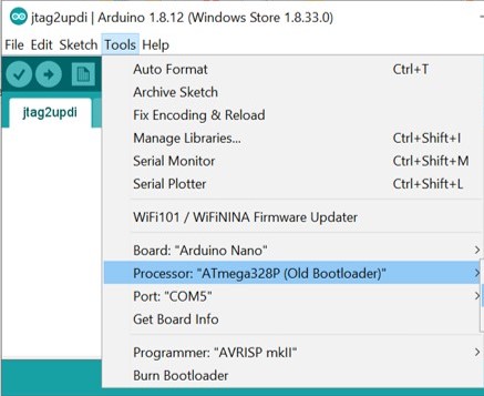
- Tools:
- Board: "Arduino Nano"
- Processor: "ATmega328P (Old Bootloader")
- Port: COM"the port device connected to"
- Programmer: "AVRISP mkll"
- Verify and Upload
Fig 12. Opening the sketch jtag2updi.ino
- A warning message
jtagmkII_initialize(): Cannot locate "flash" and "boot" memories in description is spurious and can be safely ignored.
Programming the ATtiny412
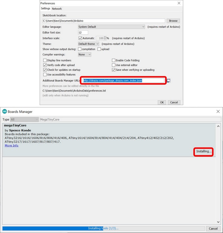
- At first, megaTinyCore should be installed via the Arduino Board Manager:
- File > Preferences or Arduino > Preferences. Locate the “Additional Board Manager URLs” text box and enter
http://drazzy.com/package_drazzy.com_index.json
- Tools>Boards>Boards manager. Enter megaTinyCore and Install it.
Fig 13. MegaTinyCore installation
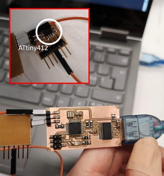
- Connect the board with ATtiny.
Fig 14. ATtiny412 connected to the new programmer
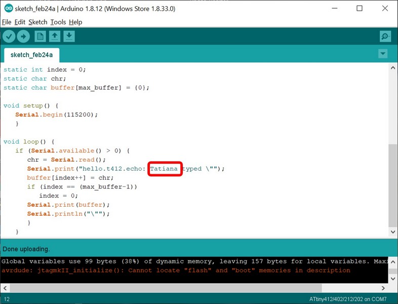
- Create New sketch in Arduino and upload
echo.ino for ATtiny412. The only change made in the sketch:
Fig 15. Programming ATtiny412
- Upload the sketch. Now the programm should be written on the ATtiny412 microchip.
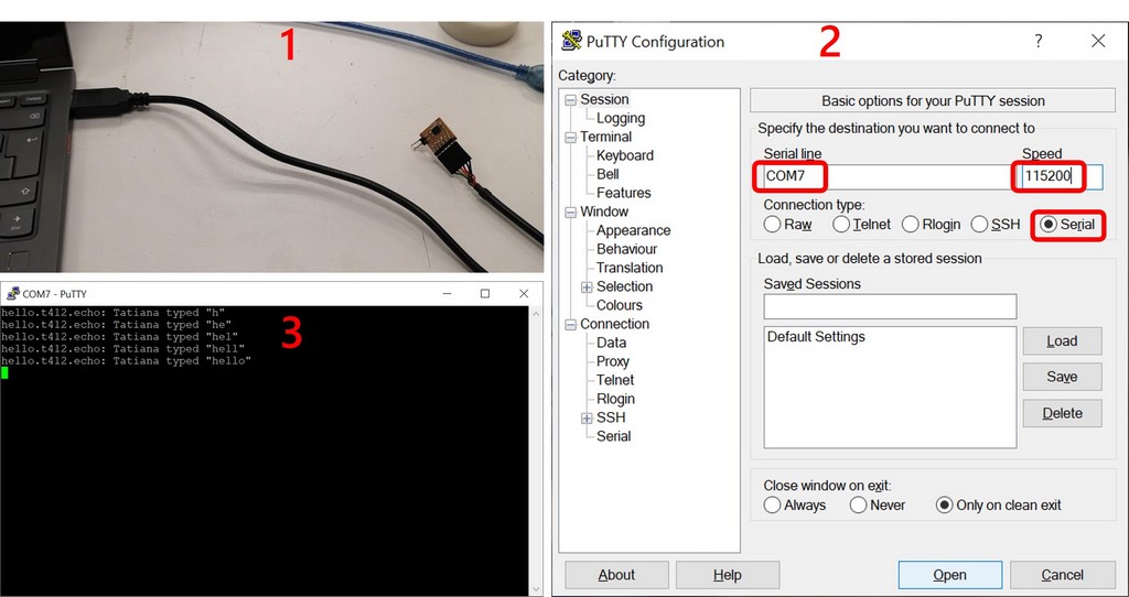
- To check the program:
-
Disconnect the programming board and connect the ATtiny412 microchip board via USB cord.
-
Download and start PuTTY with parameters highlighted below. Start typing in the new window.
Fig 16. ATtiny412 performing the programm programmed on it.
Reflection
This week again brought so much new things I thought I will never do in my life. The challenging moment for me is to understand why did we use these exact parts, what are they, how they work, and why did we connected in some cirtain way. The rest of the routine requires some skills, which I think will come with time.
