6. Electronic Design
Week’s Assignments
Group Assignment:
● Use the test equipment in your lab to observe the operation of a microcontroller circuit board.
Individual Assignments:
● Redraw the echo hello-world board.
● Add (at least) a button and LED (with current-limiting resistor).
● Check the design rules, fabricate it, and test it.
Group Assignment:
Group:
● - Xinhui Hu
● - Zhengya Gong
● - Yazan Barhoush
● - Noora Nyberg
The group assignment of this week focused on using test equipment in our lab to observe the operation of our microcontroller circuit boards, which are the ATTINY 412 echo-hello world boards we made for individual assignments.
We used a Tektronix TBS 1202B-EDU Digital Oscilloscope as the testing device, which can detect and analyze analog and digital signals for decoding and debugging. Tektronix oscilloscope has a user-friendly interface, as shown in the following figure.


Step1: Calibration
Before testing the signals, the oscilloscope needs to be calibrated. Connecting both positive and negative probes to the device as shown in the next figure and then pressing Autoset will set the device ready to be used.

Step 2: Connection The testing board needs to be connected to both the computer via PuTTY and the oscilloscope.
The echo board was first connected to the oscilloscope in the next configuration:

Then, we connect the board to a computer using PUTTY.

In the group activity, we tested the signals from three pins on the board:
● 1. GND-GND, Probe- pin POWER: 5V on the oscilloscope
The signal from this pin shows the power of the board.

● 2.GND-GND, Probe-pin TXD [Receiver]:
The signal from this pin shows what does the board receives from a computer.

● 3.GND-GND, Probe-pin RXD [Sender]:
The signal from this pin shows what does the board sends back to the computer.

Typing a letter in PUTTY command prompt the binary format of the letter that appears on the screen of the oscilloscope, as shown in the following figure. We read the ASCII code for them in the serial format.

ASCII data format implies that the order of the bits are a zero start bit, the 8 bit data from LSB (least significant bit) to MSB (most significant bit) and a one stop bit. If we adjust the scope properly, we can see that signals show clear patterns of bits.

For example, this figure shows the signal that the board sends back to the computer, which should contain this piece of information: hello.t412.echo:[board name] typed “[character]” The shown ASCII code serial should be read from right to left (from MSB to LSB). According to our setting, the first character should be “h”. As we can see in the analysis, the binary code appears as “01101000” = 104 and indeed stands for “h”.

Individual Assignments:
I used Eagle as the PCB design software for my project. Antti gave us a link to download the software and the file. He also gave the lecture about the basic rules of PCB design and assisted us in getting started with Eagle. After installing Eagle, we needed to add the FabLab components library to it. To accomplish this, I copied the file fab.lbr, and put it in the “library” folder of my Eagle. To activate the library, select it from the left menu, right click on it and check the ‘use’ box or left click the black dot to turn it to a green dot.

Schematic
● Step1. Creating a new project in Eagle from File > New > Project.
● Step2. Right click on my new project in the left menu, then New > Schematic.


● Step3. Adding the components needed from eagle_fab library, with Add Part tool.

But in this step, we did many steps, because the main component was not on the fab.lar list. First open the snapeda page then enter keywords-attiny412, choose ATTINY412-SSN. Second, generate the PIN names, numbers, and type, then click generate part, and download it for eagle. Third, put the new lbr file in library.


● Step4. After added the components, using the net tool to connect the components and add a value to 3 components.


Layout
● Step1. Go to board editor by clicking on Generate/Switch to board icon.

● Step2. Click on Move icon in the left menu to move the components to their place.

● Step3. Define the Design Rules Check (DRC) parameters (e.g. minimum clearance) from Tools > DRC. The minimum clearance cannot be less that the diameter of the milling bit that you plan to use.

● Step4. Set the Wires’ width to 16mil and connect the component with the Route tools from left menu. Make sure that you are working on the Top layer.

● Step5. When the routes between the components are ready, modify the size of the board. The board area is defined by the dimension layer (layer 20). Simply drag it to change it to your desired size.

After this step, we found the ATTINY412-SSN was not suit for the project, so Antti using -[Component Search Engine] (https://componentsearchengine.com/)generated and uploaded the ATTINY412-SSNR.lbr to the gitlab, and we downloaded it to replace ATTINY412-SSN and redo the step2 to step 5.

● Step6. Using the Dimension tool the size of the board can be checked. We saved the space for 6 Pin header positioning.

● Step7. To make the ground fills. First, Click on the polygon icon in the left menu and it close to the starting point. A polygon with a dashed line will appear. Second, to connect the polygon to ground, right click on the dash line and select Name. Name GND . Third, click on Ratsnest icon in the left menu.

● Step8. To make the outline. First, set the working layer to Milling (layer 46), and draw the the outline with Line tool from the left menu. Outlines must be thicker than the diameter of the milling tool. Since for cutting, we usually use the 1mm milling bit, I set the outlines width 40mil.

● Step9. To check by the Design Rules Check (DRC) parameters, if it did not shown errors, we can export the trace and outline. But if it shown errors, we should edit the project according to tips.
● Step10. To export the trace and outline.
The traces: 1. Hide all the layers except the Top layer from View > Layer settings. 2.Go to File > Export > Image then set the resolution to 2400dpi and select the monochrome.

The outline: 1. Hide all the layers except the 46 layer from View > Layer settings. 2.Go to File > Export > Image then set the resolution to 2400dpi and select the monochrome.

Create the rml files
I used the mods to create rml file, and steps are same as the 4 week assignment
● Select png file and press invert.
● Select the process from process > PCB traces (1/64).
● Select SRM-20 as the milling machine. Set the speed to 4mm/s and origin (x0, y0, z0) to zero and outputs to inputs.
● Set the tool diameter (I used a 0.4mm flat milling tool), the cut depth to 0.1016mm, the offset number to 4, offset step-over number to 0.5.
● Press the calculate button, and the file was download automatically.


For producing the outline file, the process is more or less the same, setting cut depth to 0.6 mm, offset number of 1 and the max depth to 1.7mm, and the most important is to change the milling bit, from 0.2mm-0.5mm to 1.00mm.


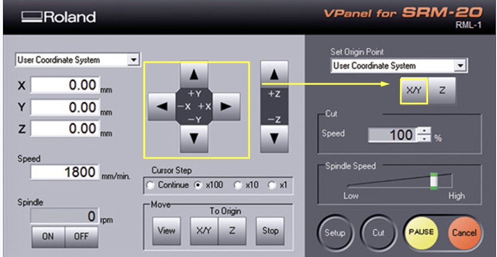
Milling board
Adjust X/Y origin: The X/Y origin determines the start point on the flat PCB board. The X/Y direction buttons can be used to adjust the X and Y coordination of the milling bit. After reaching the ideal location, click Set Origin Point >> X/Y to set the current coordination as X/Y origin.
Adjust Z origin Z coordination determines the depth of the milling bit.
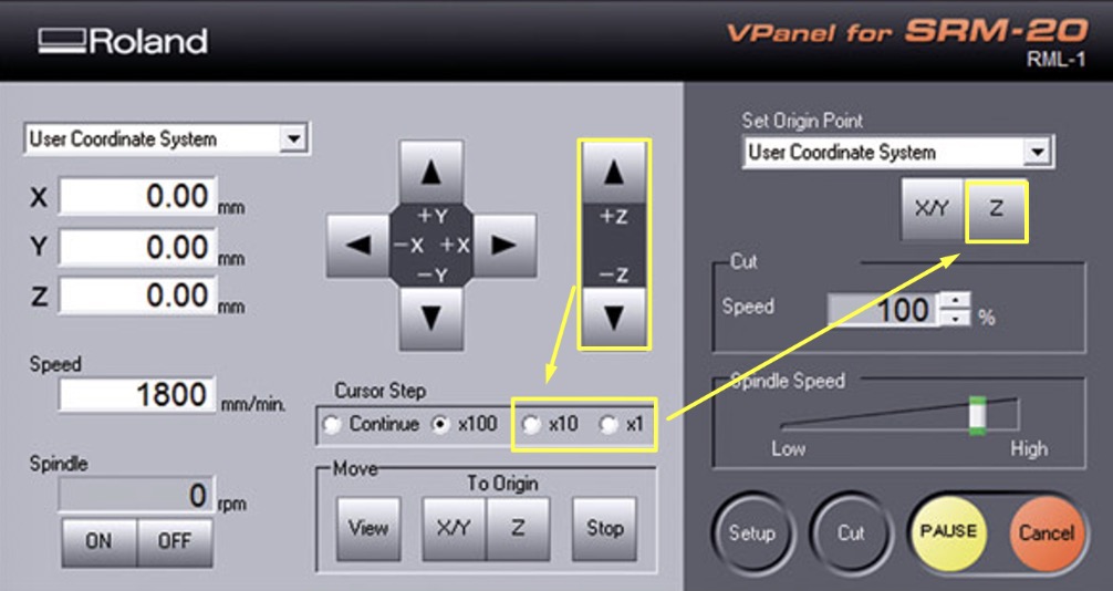
● Use the Z direction button to lower the milling bit until it is close to the PCB board without touching it. Select a small cursor step when the milling bit comes close to the board.
● Hold the milling bit with one hand and use the hex key tool to gently release it with the other hand. Carefully let the tip of the milling bit touch the surface of the board and fasten it again.
● Click Set Origin Point >> Z to set the current height as the Z origin.
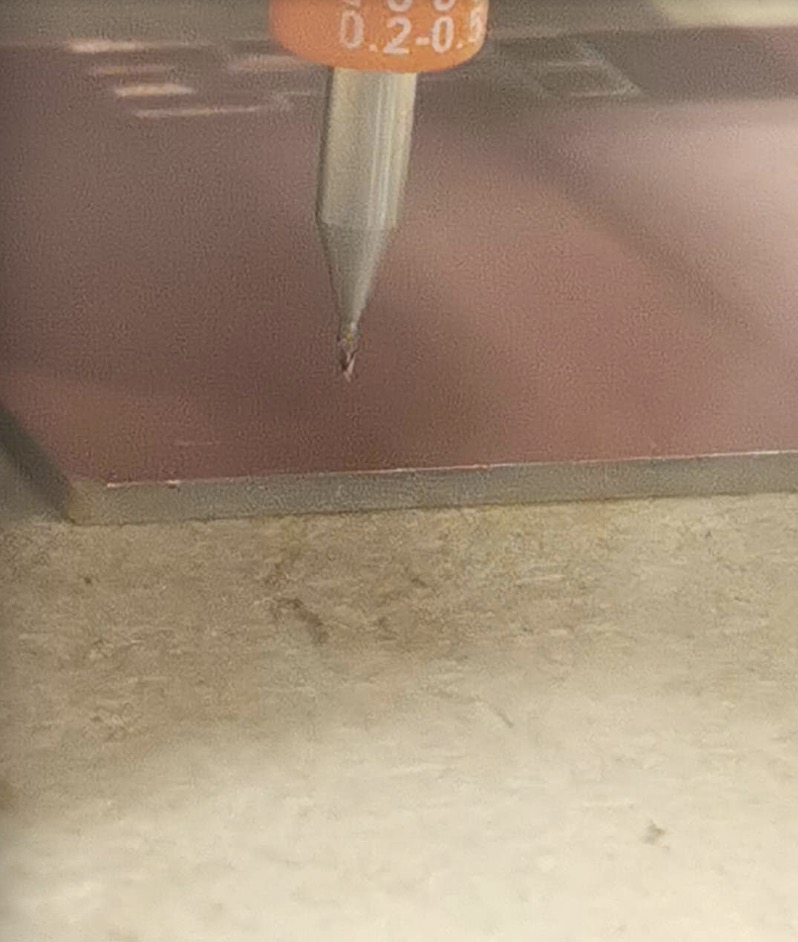
For V-shape milling bit, it is necessary to calibrate how deep it cuts into the board. Rise Z for 0.3 mm and set the location as the new Origin Point of Z and test the cut depth with the rml files saved from mods.
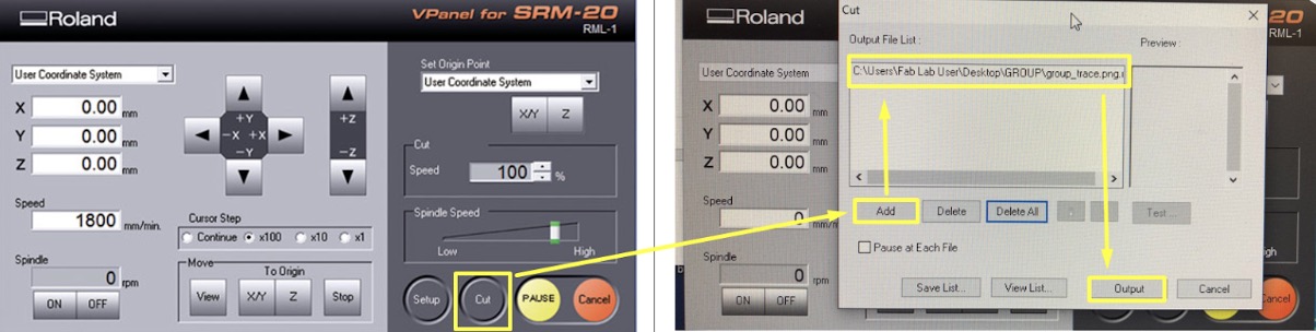
● Start the cutting task by Cut >> Add >> Select corresponding file >> Output. (The cutting task will start immediately after clicking “Output”, please double check everything before that).
● Pause and Cancel the task if milling bit is not touching the PCB board, which is expected to happen in the early rounds of calibration. In order to recalibrate, Click View >> To Origin >> Z to bring the milling bit back to its previous position. The order here is very important. Users must click “View” (which will bring the board forward) before clicking “To Origin Z”, otherwise the milling bit may be broken.
● Use the Z direction button to further decrease the height of the milling bit by a small amount, reset Z origin and restart the test task. Repeat the routine until the milling bit cuts into the PCB board with appropriate depth. This depth will be set as the final origin of Z for this milling task.
Milling bits:
● Connect Milling bits
To connect the cutter, hold Milling bits between our fingers and insert it in the place. Then use a hex wrench to tighten it.
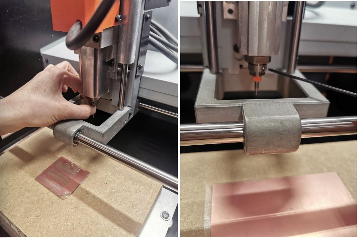
● Loosen the Milling bits
When we had been set up the XYZ, we need to loosen the Milling bits shown as figure.
Then cut it and waiting.

Soldering the Components
● Using the components list to find the components

● According to the Schematic to soldering it.

Programming
Although this is not my first time to programming, I also confused on it, and thanks Antti patience teachings, I know how to do it.
● Step1. Download the software Arduino, and because I used it on the fourth week, I have been installed it on my laptop.
● Step2. Click the code from schedule, 2020 Fab Academy, and copy it.
● Step3. Open Arduino, create a new file, and paste the code here.

● Step4. Set up the preference, and copy the URLs (http://drazzy.com/package_drazzy.com_index.json) here.

● Step5. Set up the tools. First, tools-board-board management. Second, search key words, such as Tiny and megaAVR and click install. Third, tools-board and click the ATtiny412/402/212/202/, chip-ATtiny412, Port-(my board).

● Step6. Click the verity and upload.

Testing
● Step1. Download and Open the Putty, and connect the pcb board. Then set up serial line, speed, connection.

● Step2. Just type what I want.
