9. Input Devices
Assignment
Individual assignment 1 :
● measure something: add a sensor to a microcontroller board that you have designed and read it
Group assignment:
● probe an input device’s analog levels and digital signals
Group assignment
Group:
● - Xinhui Hu
● - Zhengya Gong
● - Yazan Barhoush
● - Noora Nyberg
More details click Group assignment
Individual assignment:
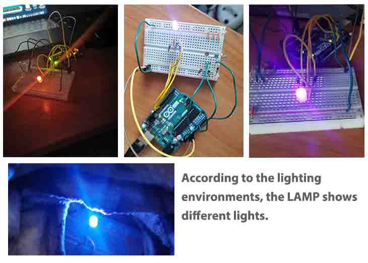
This week I used a tri-color Led and three photoresistors and created a lamp that smoothly changes colors according to lighting conditions.
Because of the virus, the fab lab closed two weeks ago; everyone stays home working remotely, so I need to design something independently. It is not easy for me to add a sensor to a microcontroller board, but fortunately, Ari sent me Arduino Projects Book, which helps me follow the book to design the lamp.
● Step 1. Find out the components. Maybe it is easy for individuals who are familiar with electronics; however, for me, I even can not identify the different resistors. Therefore, I googled the keywords, and watch some video.
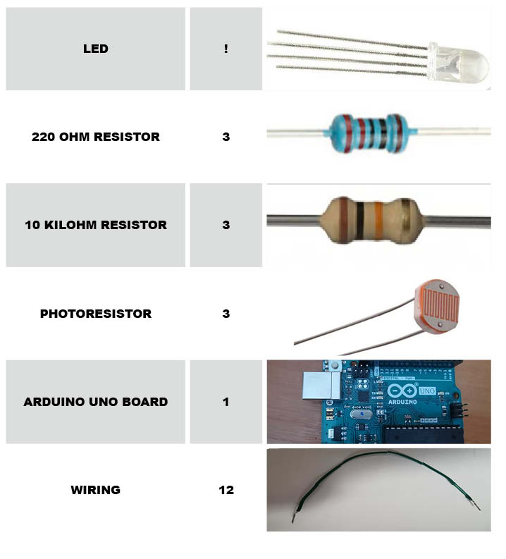
Figure 1. The components
● Step 2. Build the circuit.
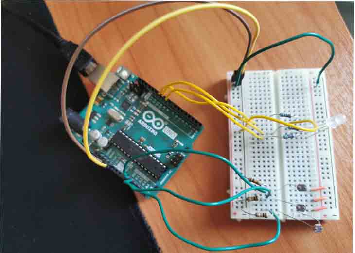
Figure 2. The circuit
● Step 3. Connect to my laptop. I used the USB cable to connect the Arduino board to my laptop. I opened the Arduino IDE and set all settings as shown in the tool.
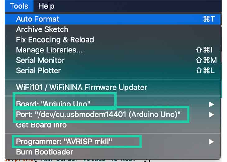
Figure 3. The tool setting
● Step 4. Programming.
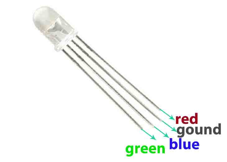
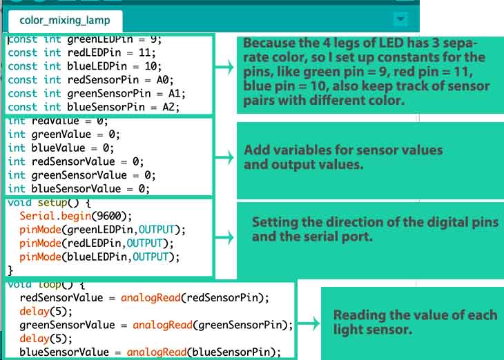
Because the 4 legs of LED has 3 separate color, so I set up constants for the pins, like green pin = 9, red pin = 11, blue pin = 10, also keep track of sensor pairs with different color.
Code Example
const int greenLEDPin = 9;
const int redLEDPin = 11;
const int blueLEDPin = 10;
const int redSensorPin = A0;
const int greenSensorPin = A1;
const int blueSensorPin = A2;
int redValue = 0;
int greenValue = 0;
int blueValue = 0;
int redSensorValue = 0;
int greenSensorValue = 0;
int blueSensorValue = 0;
void setup() {
Serial.begin(9600);
pinMode(greenLEDPin,OUTPUT);
pinMode(redLEDPin,OUTPUT);
pinMode(blueLEDPin,OUTPUT);
}
void loop() {
redSensorValue = analogRead(redSensorPin);
delay(5);
greenSensorValue = analogRead(greenSensorPin);
delay(5);
blueSensorValue = analogRead(blueSensorPin);
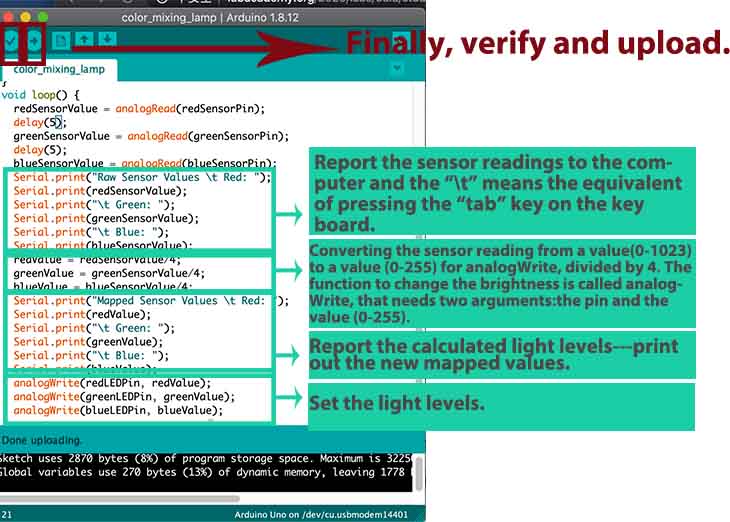
Serial.print("Raw Sensor Values \t Red: ");
Serial.print(redSensorValue);
Serial.print("\t Green: ");
Serial.print(greenSensorValue);
Serial.print("\t Blue: ");
Serial.print(blueSensorValue);
redValue = redSensorValue/4;
greenValue = greenSensorValue/4;
blueValue = blueSensorValue/4;
Serial.print("Mapped Sensor Values \t Red: ");
Serial.print(redValue);
Serial.print("\t Green: ");
Serial.print(greenValue);
Serial.print("\t Blue: ");
Serial.print(blueValue);
analogWrite(redLEDPin, redValue);
analogWrite(greenLEDPin, greenValue);
analogWrite(blueLEDPin, blueValue);
}
The function to change the LED’s brightness via PWM is called analogWrite(). It needs two arguments: the pin to write to, and a value between 0 - 255. This second number represents the duty cycle the Arduino will output on the specified pin. A value of 255 will set the pin HIGH all the time, making the attached LED as bright as it can be. A value of 127 will set the pin HIGH half the time of the period, making the LED dimmer. 0 would set the pin LOW all the time, turning the LED off. To convert the sensor reading from a value between 0 - 1023 to a value between 0 - 255 for analogWrite(), divide the sensor reading by 4.
● Step 5. Testing.
Individual assignment 2(for final project):
For my final project, in this week I created a circle (integrated with input, output device and networking and communication)and designed my PCB board, the test and programming in - output device week.
● Step 1. Download and read components data sheet.
By reading the data sheet, I learned that so much information about the product is included in Data Sheet. There is really a lot of information in the data sheet. Too much for a beginner like me to actually get into unless I know what I’m looking for. The pinout is very important.
HX711 Balance Module With Load Cell data sheet
This module uses 24 bit high-precision Analog to digital converter. This chip is designed for high-precision electronic scale and design, has two analog input channels, programmable gain of 128 integrated amplifier. The input circuit can be configured to provide a bridge voltage electrical bridge (such as pressure, load) sensor model is an ideal high-precision, low-cost sampling front-end module.
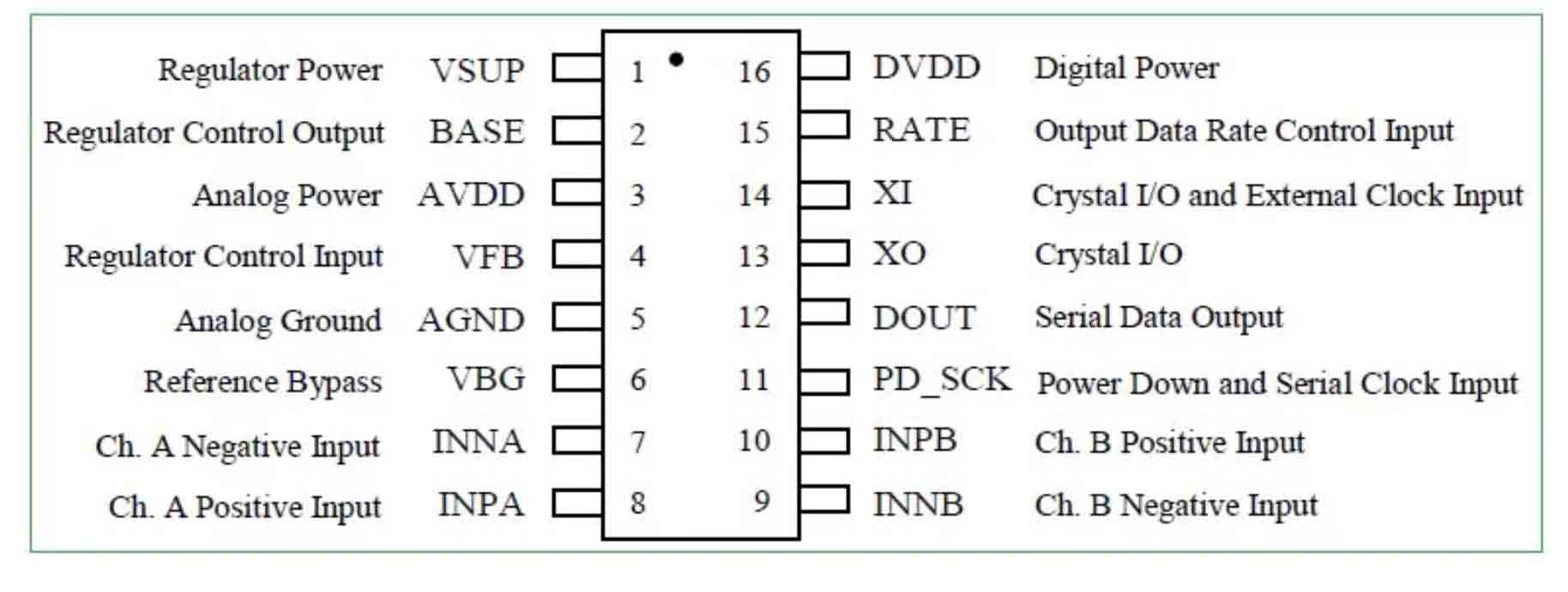
● HX711 Pin Description
● Load Cell Wire Connection
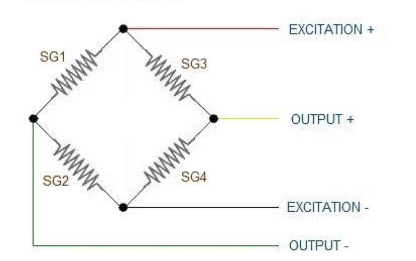
Load Cell to HX711
E+ : WHITE
E- : BLACK
A- : RED
A+ : GREEN
HX711 to STC89C52
GND:GND
VCC:VCC
SCK:P13
DT:P12
STC89C52 data sheet
STC89C52 is fully compatible to the standard 8051 microcontroller, maintains all instruction mnemonics and binary compatibility. STC89C52 can run 6 (as the same as the standard 80C51) or 12 clocks per machine cycle. Improvement of individual programs depends on the actual instructions used.
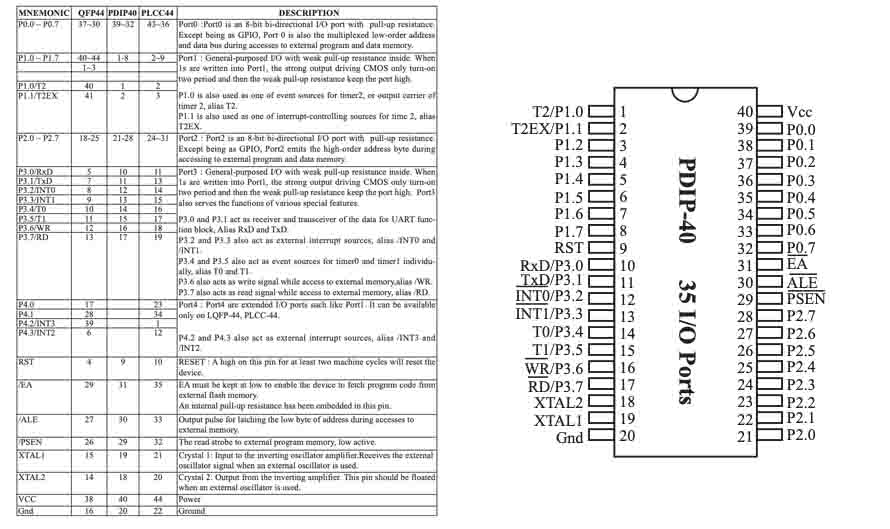
Pin description of STC89C52
● 1. Main power pin VCC and VSS
The power supply VCC is connected to +5V, and the VSS ground terminal is the public reference ground
● 2. Clock circuit pins XTAL1 and XTAL2
STC89C52 chip is equipped with an inverter amplifier, and XTAL1 is the input terminal of the amplifier. XTAL2 is the output end of the amplifier and the input end of the internal clock generator. When using the self-excited oscillation mode, XTAL1 and XTAL2 are externally connected with quartz crystal oscillator, and the internal oscillator oscillates according to the crystal oscillator frequency to generate clock signal.
● 3. Control signal pin
-(1)RST – reset input. When the oscillator is working, the RST pin with a high level of more than two machine cycles will be the MCU reset.
-(2)ALE/PROG – when accessing external program memory or data memory, ALE(address latches allow) outputs pulses of the lower 8-bit bytes used to lock the address. In general, ALE still outputs a fixed pulse at 1/6 of the clock oscillation frequency, so it can output a clock or be used for timing purposes. Note that a ALE pulse is skipped each time the external data store is accessed. (generally not used)
-(3)PSEN – program storage allowed (PSEN) output is the read selected communication number of external program memory. When STC89C52 fetches instructions (or data) from external program memory, each machine cycles PSEN twice, that is, outputs two pulses. During this period, when accessing external data memory, PSEN signals will be skipped twice.
-(4)EA/VPP – external access allowed. To enable the CPU to access only external program memory (address 0000h-ffffh), the EA terminal must remain low (grounded). Note that if the encryption bit LB1 is programmed, the state of the EA end will be locked internally during reset. If the EA end is at a high level (connected to the Vcc end), the CPU executes instructions from the internal program memory. When programming FLASH memory, the pin plus +12V programming allows the power supply Vpp, of course it must be that the device is using 12V programming voltage Vpp.
-(5) parallel I/O port P0~P3 terminal pins
P0 port (P0.0~P0.7) 8-bit drain switch type bidirectional I/O port. It can be used as a universal I/O port, but must have a pull resistance.
P1 port (P1.0~P1.7) is an 8-bit quasi-bidirectional I/O port with pull resistance.
Port P2 (P2.0~P2.7) is an 8-bit quasi-bidirectional I/O port with pull resistance.
P3 port (P3.0~P3.7) is an 8-bit bidirectional I/O port with pull resistance.
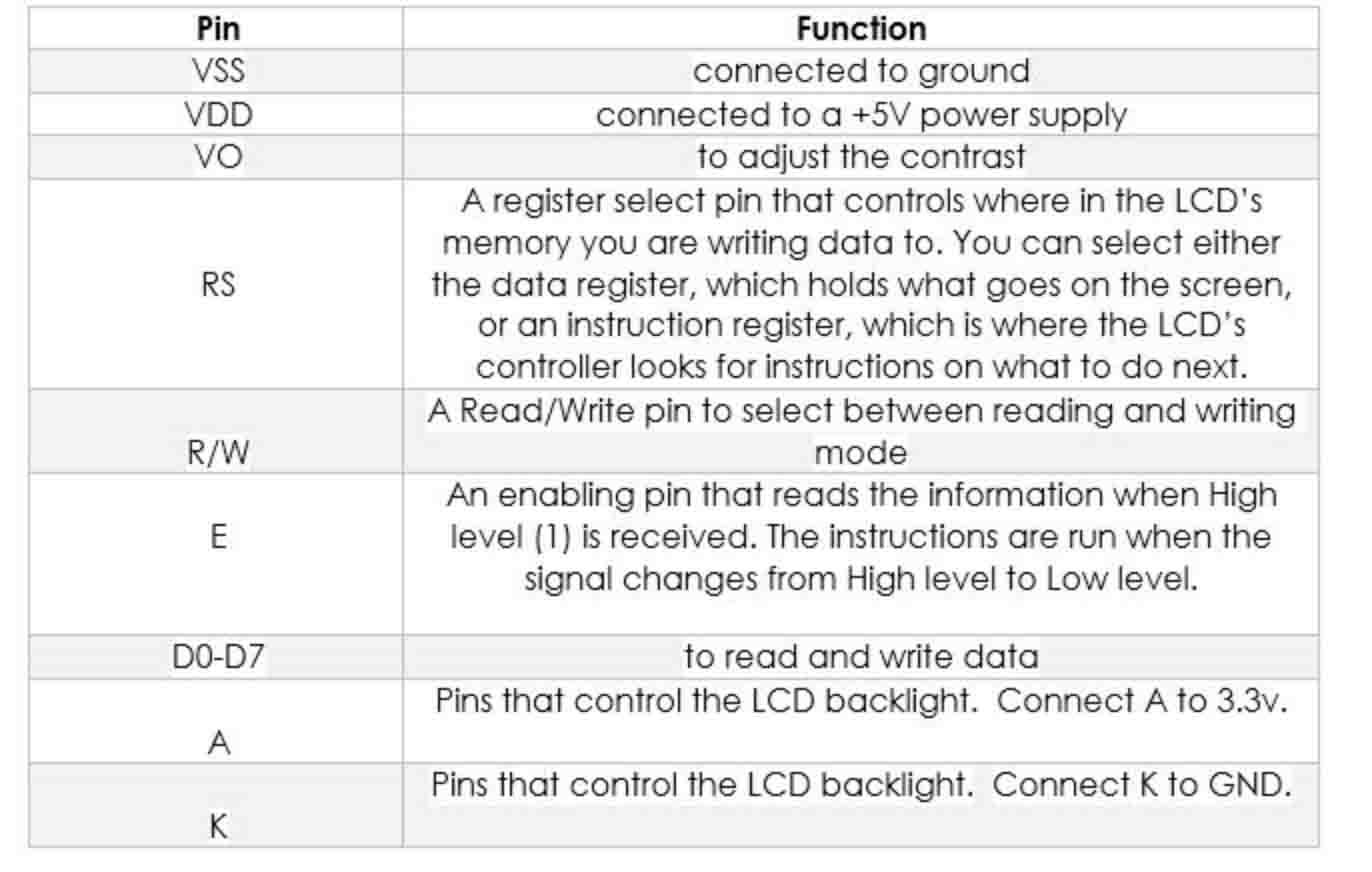
LCD1602 data sheet
LCD1602, or 1602 character-type liquid crystal display, is a kind of dot matrix module to show letters, numbers, and characters and so on. It’s composed of 5x7 or 5x11 dot matrix positions; each position can display one character. There’s a dot pitch between two characters and a space between lines, thus separating characters and lines. The model 1602 means it displays 2 lines of 16 characters. Generally, LCD1602 has parallel ports, that is, it would control several pins at the same time. LCD1602 can be categorized into eight-port and four-port connections. If the eight-port connection is used, then all the digital ports of the SunFounder Uno board are almost completely occupied.
The pins description
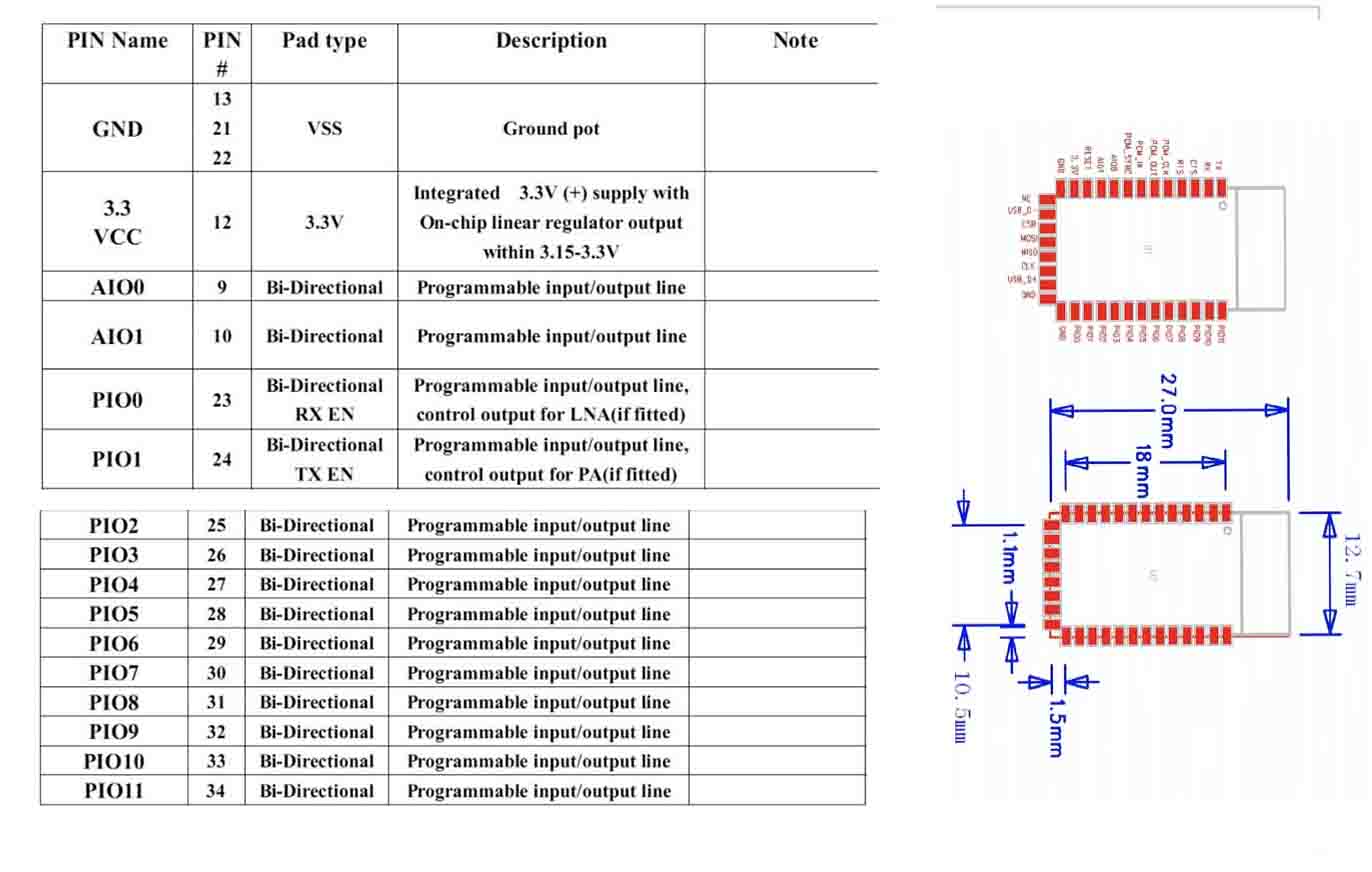
HC-5 Bluetooth data sheet
HC-05 module is an easy to use Bluetooth SPP (Serial Port Protocol) module, designed for transparent wireless serial connection setup. Serial port Bluetooth module is fully qualified Bluetooth V2.0+EDR (Enhanced Data Rate) 3Mbps Modulation with complete 2.4GHz radio transceiver and baseband. It uses CSR Bluecore 04-External single chip Bluetooth system with CMOS technology and with AFH(Adaptive Frequency Hopping Feature). It has the footprint as small as 12.7mmx27mm.
The pin description and Hardware
● Step 2. Electronic design
I am interesting in the electronic design, so I learned another software Altium designer, also used it to design my PCB board.
● Design the Schematic. I downloaded the library- Schematic library, created the new project, and created the new Schematic. Then put the components and using the line tool to connect it.
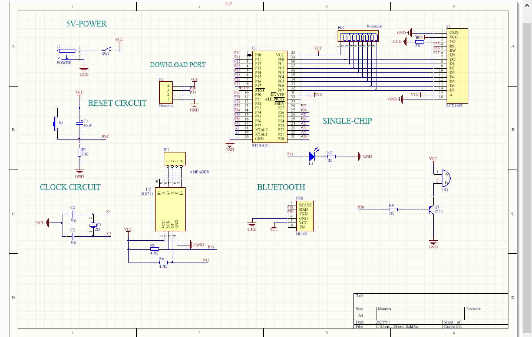
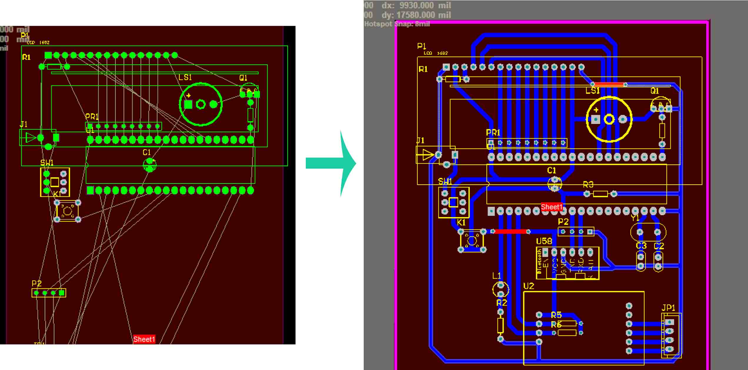
● Design the PCB board. In this stage, it is a bit of different, it should create the new PCB and selected the design >> update PCB Document.
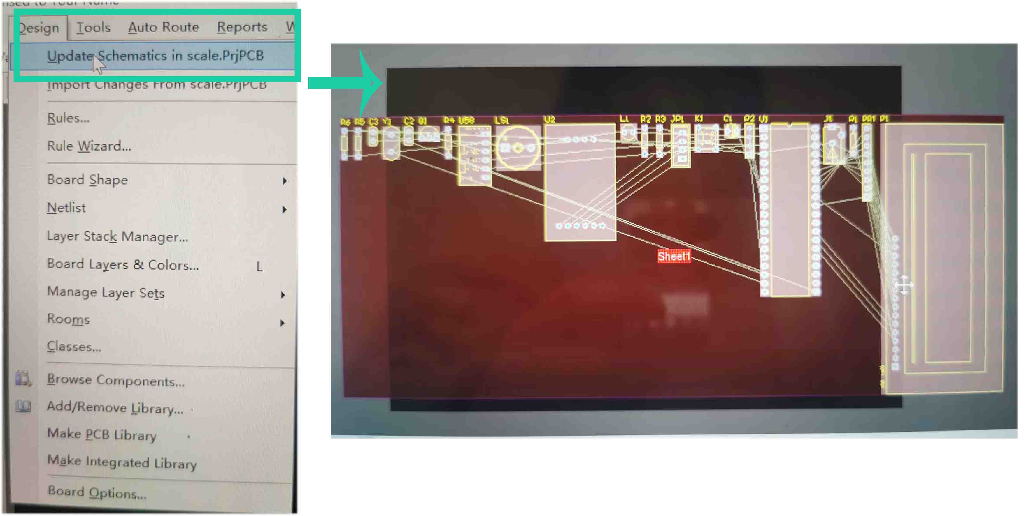
Then using Move to put the components and using line to connect the pins. Also I set the line to be 50 mil, the clearance to be 10 mil.
● When I did the design work, I save it as DWG. Also, the lines shown different color according to the color of layers.
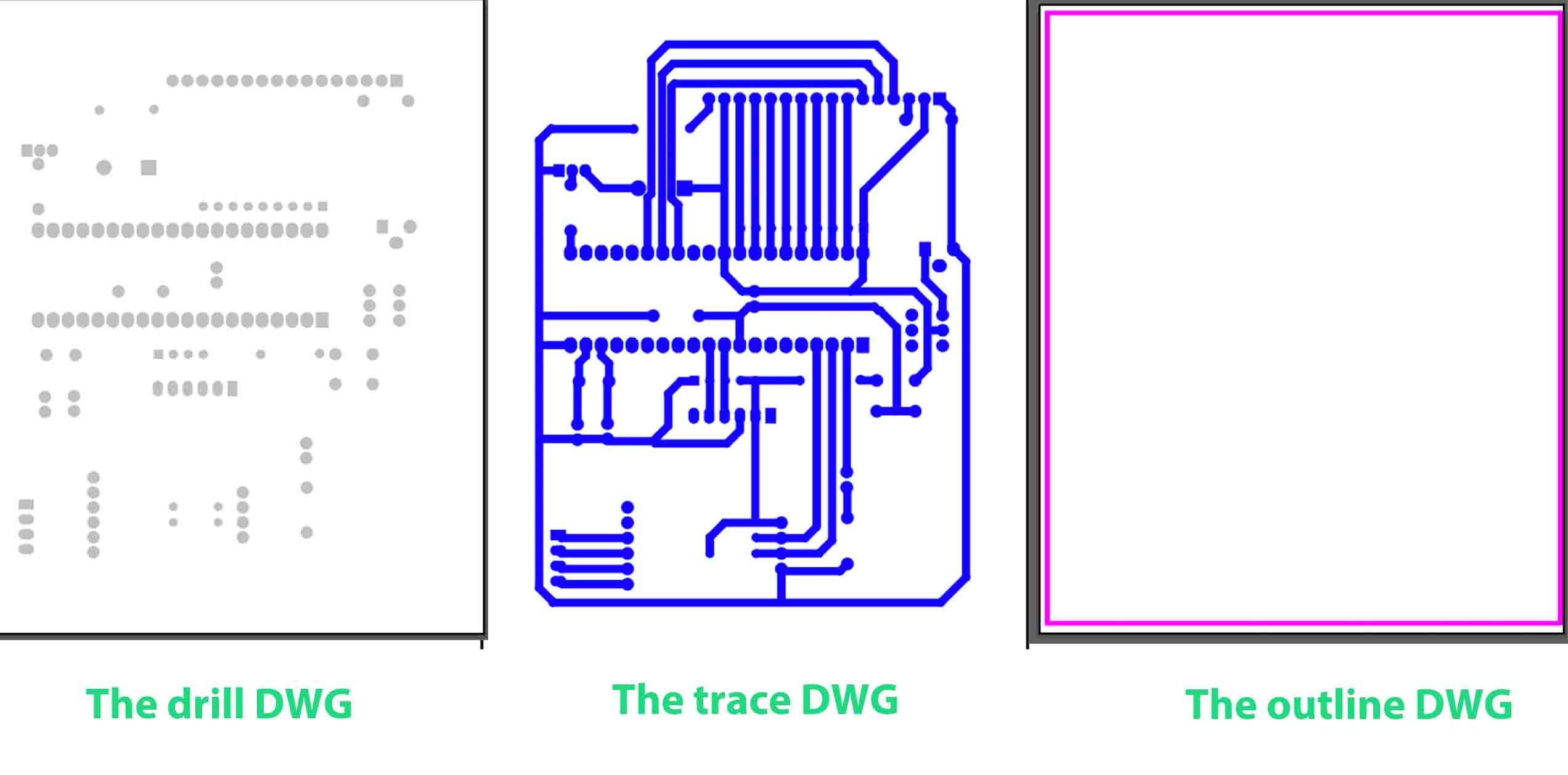
● I opened the files using Adobe Illustrator, and changed the color to be black, then mirror and save it to be PNG files.
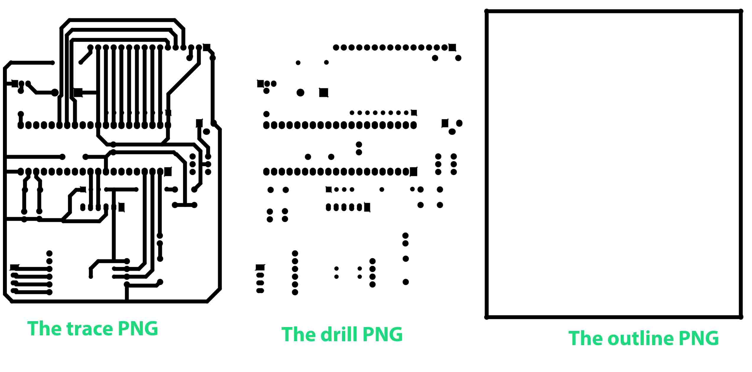
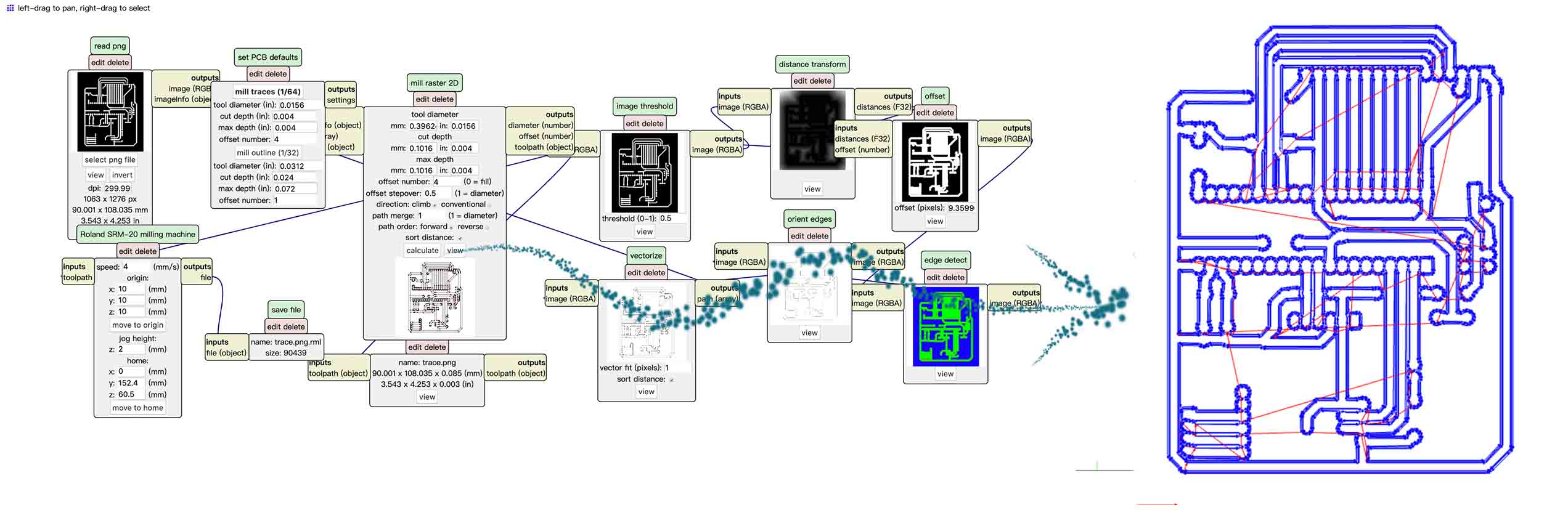
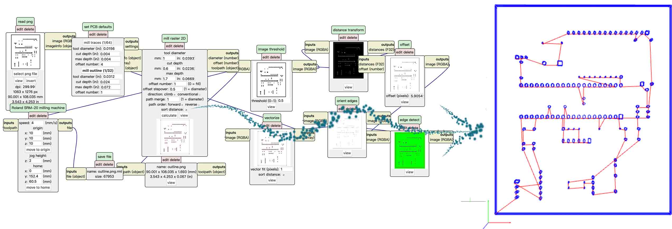
● Open mods, and set it as the 4 weekly assignmentand 6 weekly assignment. Then the rml files created and downloaded automatically.
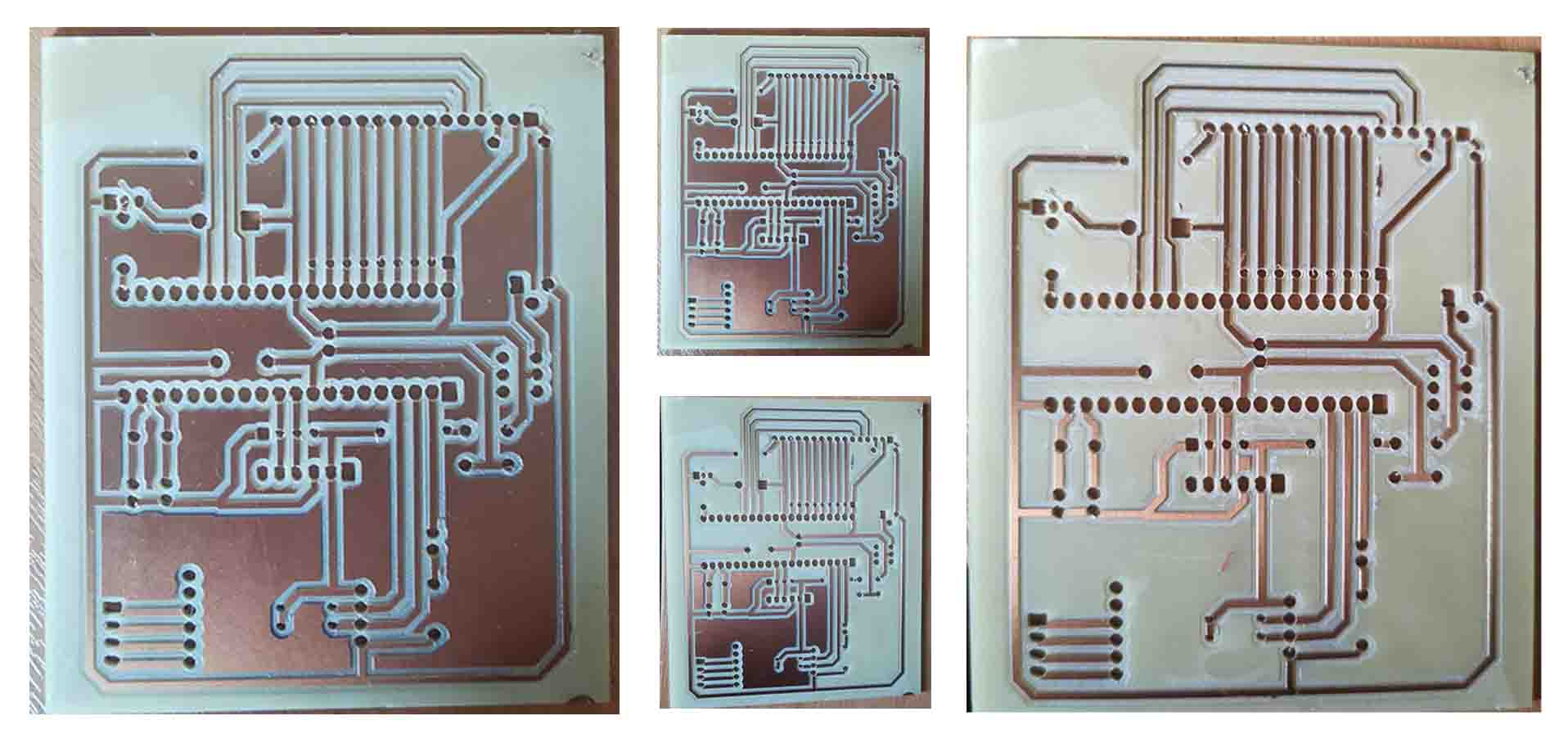
● 6. After milling the PCB board, I would like to make the Lines clear, so that I can soldering it better. I tore off the excess metal layer。
The test and programming in -output device week.