14. Networking and Communications
This week was all about multi-processors. It was the most confusing week by far. We went over the different types of multi processor communications in lecture. The different types of communications include Serial Bus (SPI, I2C and USB), OSI layers (stands for Open Systems Connection and there are seven layers) I focused on the asyncronous I2C connection and the Radio Frequency Identification module. I worked with the RFID reader on the arduino and then deisgned a board to make when I get back into the lab.
Group Assignment
The 2022 group assignment is linked here.
Lecture Notes
Why use multiple processors?
- Location: Control different components in other locations
- Parallelism: In a desktop computer, there are multiple threads running at the same time. It divides work among the processors. System of processors instead of one big one.
- Modularity: Instead of one big system, break it into many modules. Eg: one just runs the motor, one just does the display, one just talks to the container. Helps to develop and debug separately and then combine to make the system.
- Interference: May need a high current drive for a motor and a low noise for sensor, this is good for it.
I2C (Inter-Integrated Circuit)
To understand this topic better, I watched this video on youtube. It was super helpful with explaining how the I2C communication works. Here is what I got from the video:
I2C communication bus is very popular and widely used by many electronic devices because it can be easily implemented in many electronic designs which require communication between a master and multiple slave devices or even multiple master devices. This is because only two wires are required for communication between 128 devices when using 7 bits addressing and upto 1024 devices when using 10 bits addressing. Each device has a preset ID or a unique device address so the master can choose with which device will be communicating. The two wires are called serial clock or SCL and serial data or SDA.
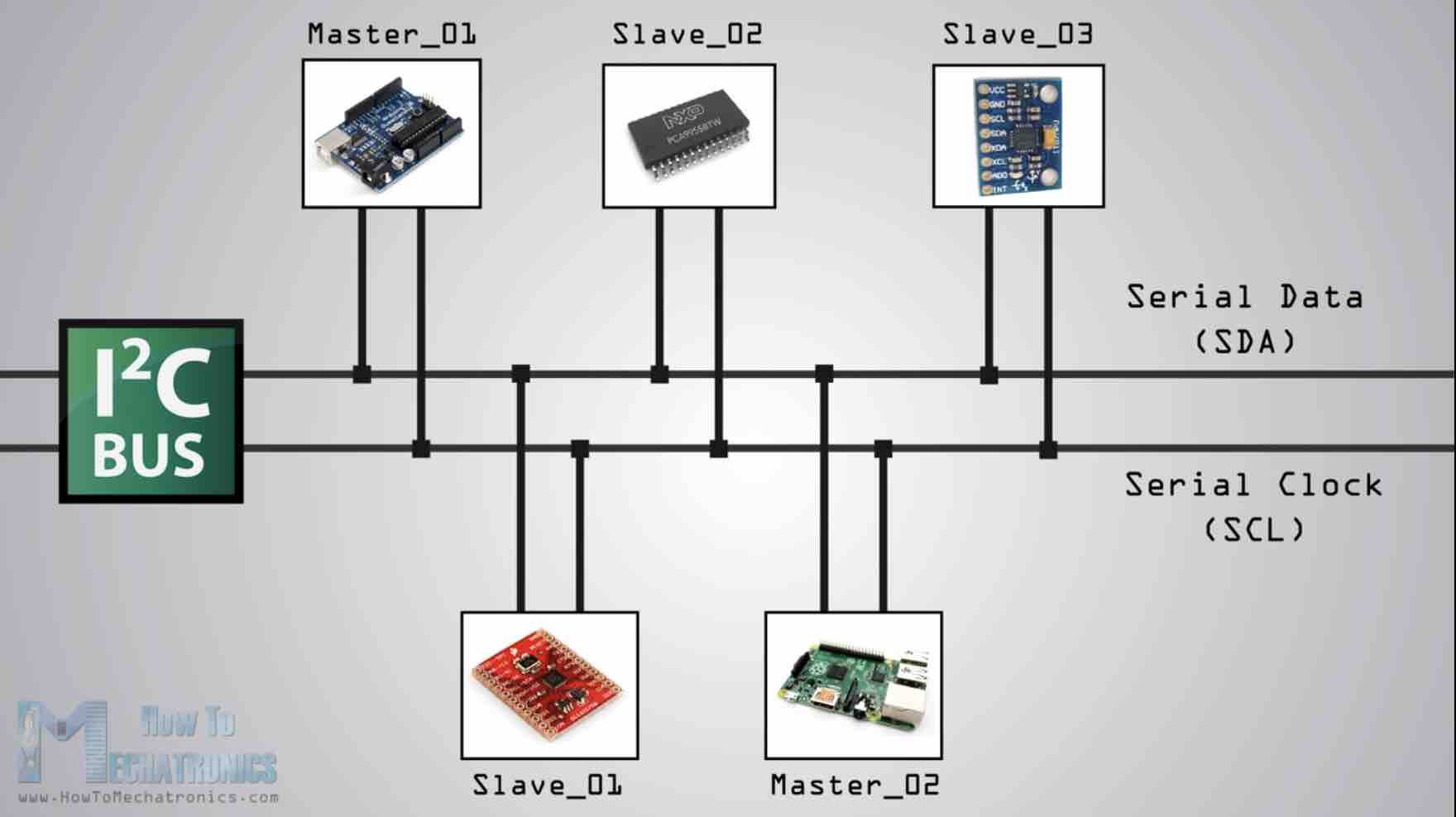
The SCL line is the clock signal which synchronizes the data transfer between the devices on the I2C bus and is generated by the master device. The SDA line carries the data.
The two lines are open drain, which means that pull-up resistors need to be attached to them so that the lines are high because the devices on the I2C bus are active flow. Commonly used values for the resistors range from 2K for higher speeds at about 400 kilobits per second up to 10K for lower speeds at about 100 kilobits per second.

The data signal is transferred in sequences of 8 bits. After a special start condition, the first eight bits sequence occurs, which indicates the address of the slave where the data is being sent. After each 8 bit sequence follows a bit called acknowledge. After the first acknowledge bit comes another addressing sequence for the internal registers of the slave device. Next follows the data sequences until the data is completely sent. It ends with the special stop condition.

RFID (Radio Frequency Indentification)
I got all the information for this section from this video.
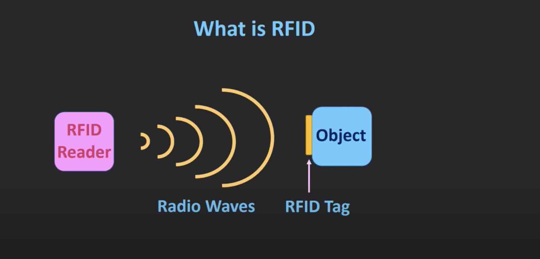
RFID is technology that works on radio frequency or radio waves. This is usually used to automatically identify or track objects. It is used in stores, car tags, library books, warehouses, to track animals etc. A RFID tag is attached to the object that you want to track. The RFID reader continuously sends radio waves. when the object is in the range of the reader, the object identifies the reader and sends a feedback signal back. Using this RFID technology, we can track multiple objects at the same time.
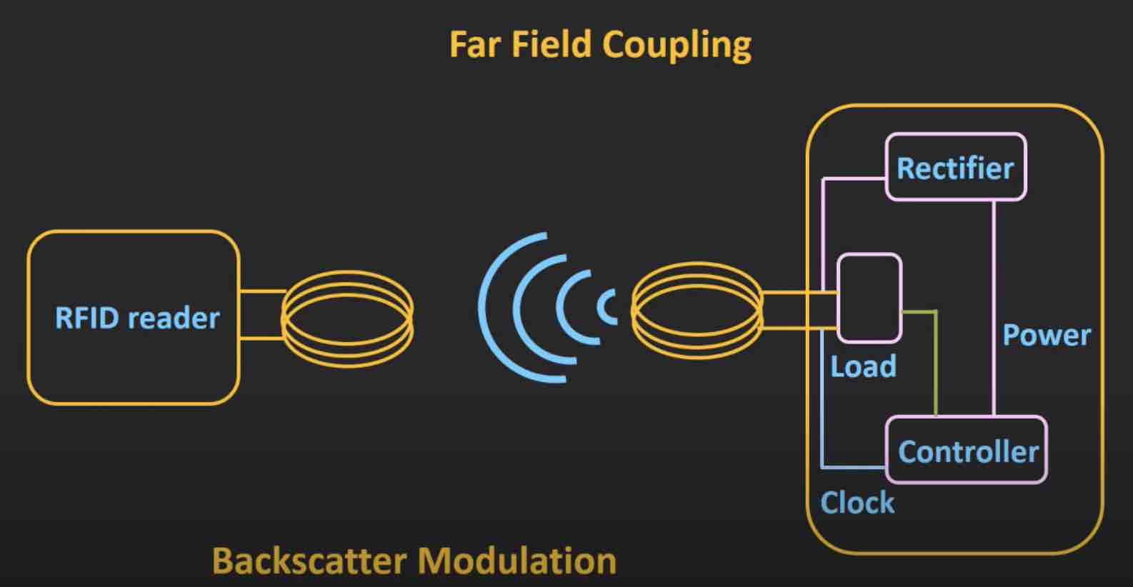
The RFID system contains 2 components, the reader and the tag. The RFID tag can be either active, passive, or semi passive. The passive tags do not have their own power supply so they rely on the radio waves coming from the RFID reader for energy. Semi passive tags use their own power supply. However, they rely on the signal coming from the RFID reader for transporting the feedback signal back to the RFID reader. Active tags have their own power supply for transmitting the signal back to the reader. Since passive tags do not have their own power supply ,the range is less compared to active and the semi passive tags.

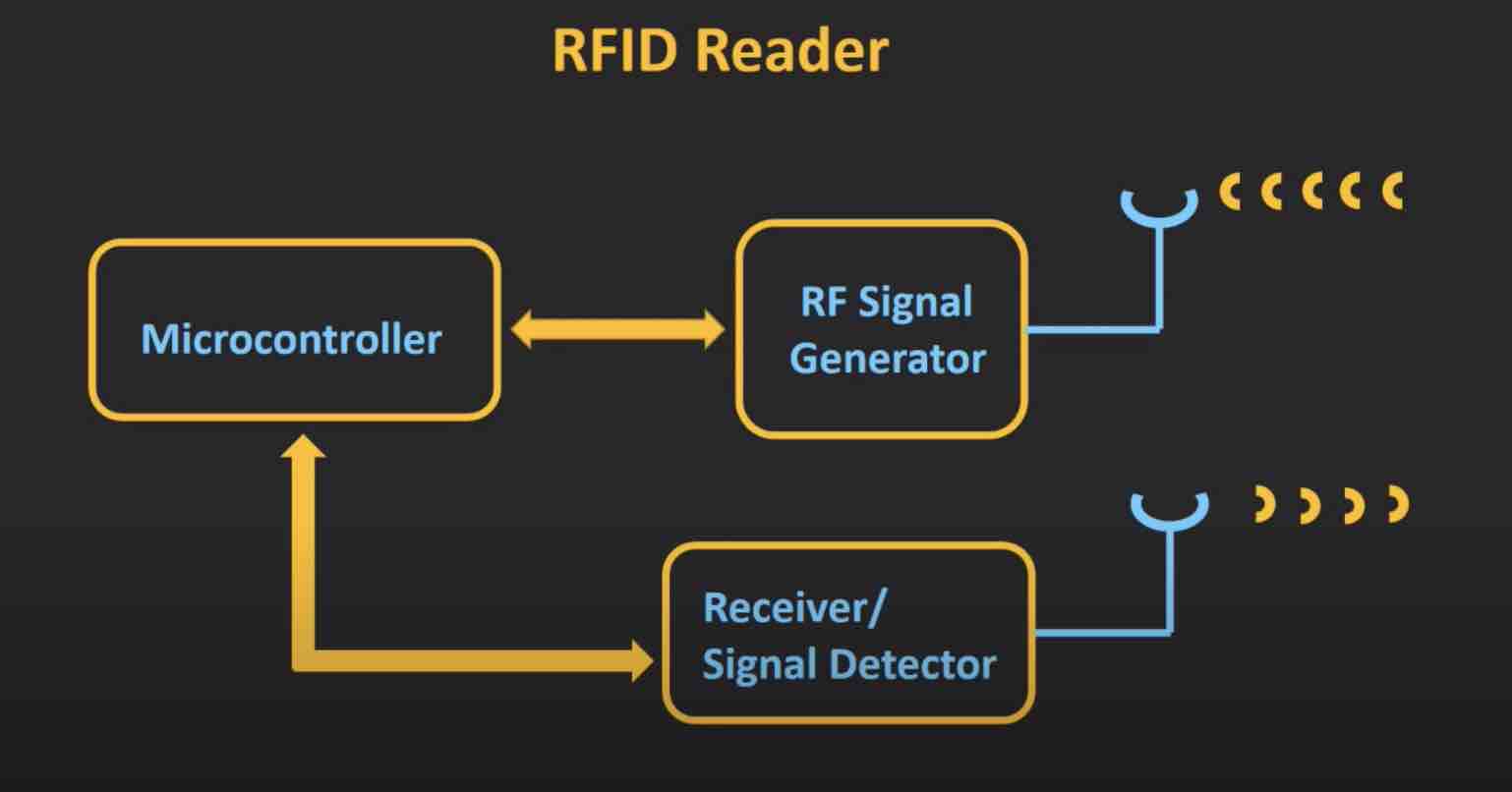
RFID readers consist of three main components, the RF signal generator, the signal detector and the microcontroller.RF signal generator generates the radio waves that are transmitted using the antenna. The receiver or signal detector receives the information coming from the tag. The microcontroller processes the information sent by the RFID tag.
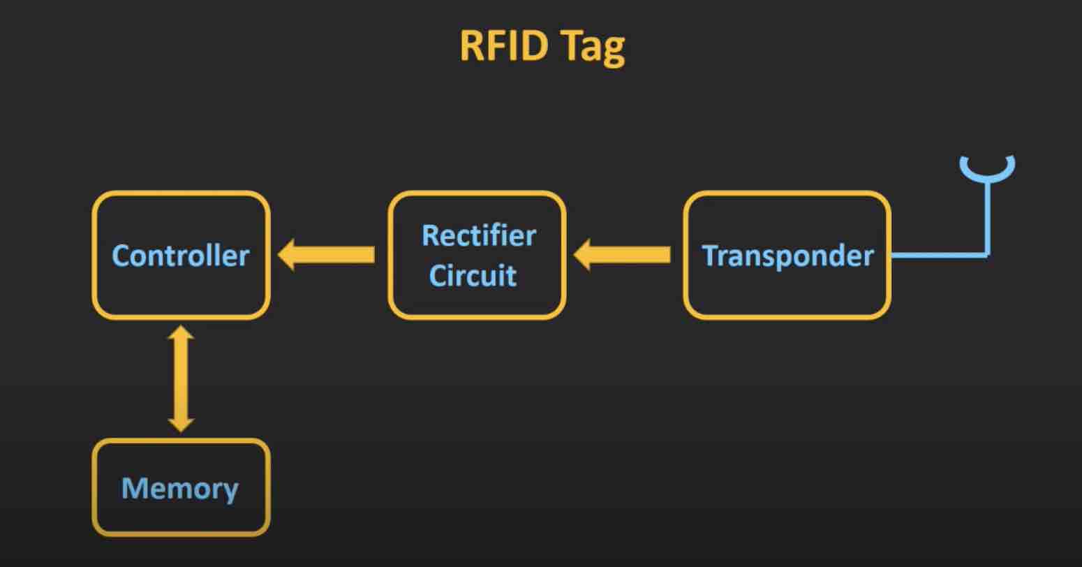
The most common tags used today are the passive tags since they are much cheaper, do not require any power source making them compact, and are versatile. The first component inside the RFID tag is a transponder. It receives the radio waves coming from the reader and sends the feedback signal back to the reader. As passive tags do not have their own supply, they rely on the radio waves coming from the reader. Using the rectifier circuit, energy from the radio waves will be stored across the capacitor. This energy is used as the supply for the controller and the memory element in the RFID tag.
The RFID tags are operated at three frequencies: the low frequency range, the high frequency range, and the ultra high frequency range. The frequency range varies from country to country. SInce low frequency signals can travel very short distances, their range is upto 10cm.High frequency signals can travel upto 1m and Ultra high frequencies can travel from 10 to 15m.

The working principle also depends upon the frequency of operation. For low and high frequency signals, the working principle is based on the inner tube coupling. For ultra high frequency RFID tags, the working principle is based on electromagnetic coupling.
The radio waves sent by the RFID reader serves three purposes: it induces enough power in the passive tag, it provides the synchronization clock for the passive tags, and it acts as a carrier for the data coming back from the RFID tag.

When the RFID tag and the reader are in range, the field generated by the RFID reader will get coupled with the antenna of the RFID tag. Due to this mutual coupling, a voltage will get induced across the coil in the RFID tag. Some portion of this voltage is getting rectified and used as a power supply for the controller as well as memory elements. Since the RFID reader is sending radio waves of a particular frequency, the induced voltage across the coil is also of a particular frequency. Therefore, this induced voltage is also used to deliver a synchronization clock for the controller. If we connect to load across the coil, current will start flowing through the load. If the impedance of the load is changed then the current that is flowing through the load will also change. If we switch the load on and off, the current will also switch on and off. This rate of change of current also generates a voltage in a RFID reader. This switching on and off of the load is known as Load Modulation.

If we switch the load on and off according to the data stored inside the RFID tag, then that data can be read by the RFID reader in the form of a voltage. Therefore, using load modulation, we are changing the voltage that is generated across the RFID reader coil. In this way, we are generating a modulation on a carrier frequency. This is how a low frequency and a high frequency RFID tags using this load Modulation technique to send data back to the RFID reader.
For Ultra high frequency, since the distance between the tag and the reader will be a few meters, it will be far field coupling. The reader continuously sends radio waves of a particular frequency to the tag. In response, the tag sends a weak signal to the reader. This weak signal is called backscattered signal and its intensity depends upon the load matching across the coil. If the load matches exactly, the intensity of the backscattered signal will be more. If the load does not match exactly, the intensity of the signal will be less. By changing the condition of the load, we can change the intensity of this backscattered signal. If we change the condition of the load according to the data that is being stored across the RFID tags, then that data can be sent back to the RFID reader. This is how the RFID reader is able to sense the data. In far field coupling, the distance between the RFID reader and tag is it a few metres, so the initial signal which is sent by the reader should be strong so that the backscattered signal can be retrieved by the RFID reader. This is the backscatter modulation technique.
Individual Assignment
The individual assignment for this week was to design, build, and connect wired or wireless node(s) with network or bus addresses. I decided to use the RFID module. I found this video tutorial on youtube. It controls two LED lights, a buzzer, and a servo motor with the RFID sensor. I decided to eliminate the buzzer and the servo motor. Therefore, the RFID sensor controls only the LED lights. If access is granted, the green LED light comes one. If access is denied, the red LED lights up.
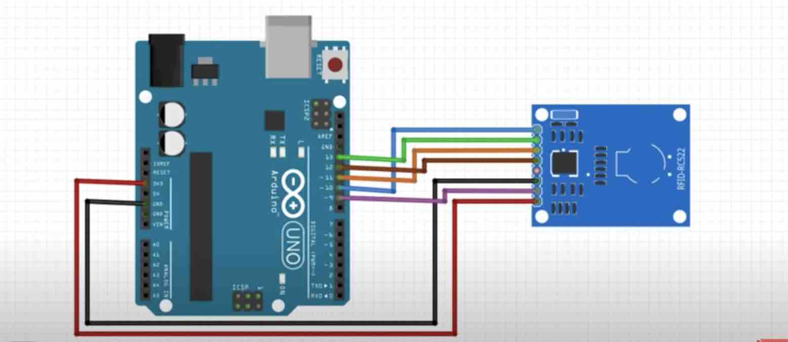
First up, I had to install the MFRC522 library. This can be done by going to sketch –> Include Library. Search for the appropriate library and install it. Next, I connected the RFID reader to the arduino using the schematic below:
Connect it to the computer and open Arduino. Open the “Dumpinfo” code from the MFRC522 library. This is the path:

The code tells you where to connect the pins on the RFID reader. Crosscheck the connections here. Upload code to the board.

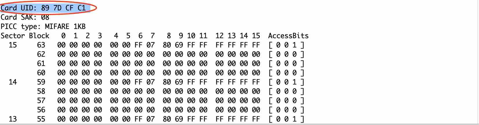
Once the code is uplaod, bring the tag close to the reader. The reader picks up the signal and spits out information about the tag. Note the Card UID number. Do this for the card as well.
Next, connect the two LEDs. Don’t forget the pull-up resistors. Once everything is connected, upload the code below:
//RFID
#include <SPI.h>
#include <MFRC522.h>


#define SS_PIN 10
#define RST_PIN 9
#define LED_G 4 //define green LED pin
#define LED_R 5 //define red LED

MFRC522 mfrc522(SS_PIN, RST_PIN);   // Create MFRC522 instance.


void setup()
{
  Serial.begin(9600);   // Initiate a serial communication
  SPI.begin();      // Initiate  SPI bus
  mfrc522.PCD_Init();   // Initiate MFRC522
  pinMode(LED_G, OUTPUT);
  pinMode(LED_R, OUTPUT);
  Serial.println("Put your card to the reader...");
  Serial.println();

}
void loop()
{
  // Look for new cards
  if ( ! mfrc522.PICC_IsNewCardPresent())
  {
    return;
  }
  // Select one of the cards
  if ( ! mfrc522.PICC_ReadCardSerial())
  {
    return;
  }
  //Show UID on serial monitor
  Serial.print("UID tag :");
  String content= "";
  byte letter;
  for (byte i = 0; i < mfrc522.uid.size; i++)
  {
     Serial.print(mfrc522.uid.uidByte[i] < 0x10 ? " 0" : " ");
     Serial.print(mfrc522.uid.uidByte[i], HEX);
     content.concat(String(mfrc522.uid.uidByte[i] < 0x10 ? " 0" : " "));
     content.concat(String(mfrc522.uid.uidByte[i], HEX));
  }
  Serial.println();
  Serial.print("Message : ");
  content.toUpperCase();
  if (content.substring(1) == "89 7D CF C1") //change the UID of the card/cards that you want to give access
  {
    Serial.println("Authorized access");
    Serial.println();
    delay(500);
    digitalWrite(LED_G, HIGH);
    delay(5000);
    digitalWrite(LED_G, LOW);
  }

 else   {
    Serial.println(" Access denied");
    digitalWrite(LED_R, HIGH);
    delay(1000);
    digitalWrite(LED_R, LOW);
  }
}
Remember to change the UID number of the card/cards that you want to give access to. This is the final result:
This is a screenshot of the serial monitor:

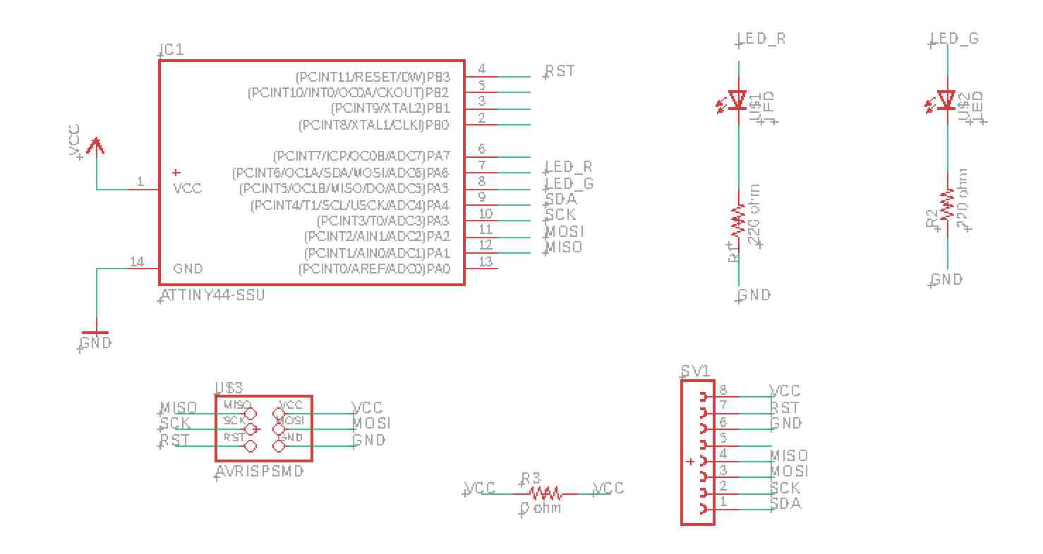
Once I had everything up and running, I attemtped to design my board on EAGLE. Here are the components that I used:
- ATTiny 44
- Red LED
- Green LED
- 220 ohm resistors X2
- 0 ohm resistor as a jumper
- AVR ISP header
- 1X8 female header
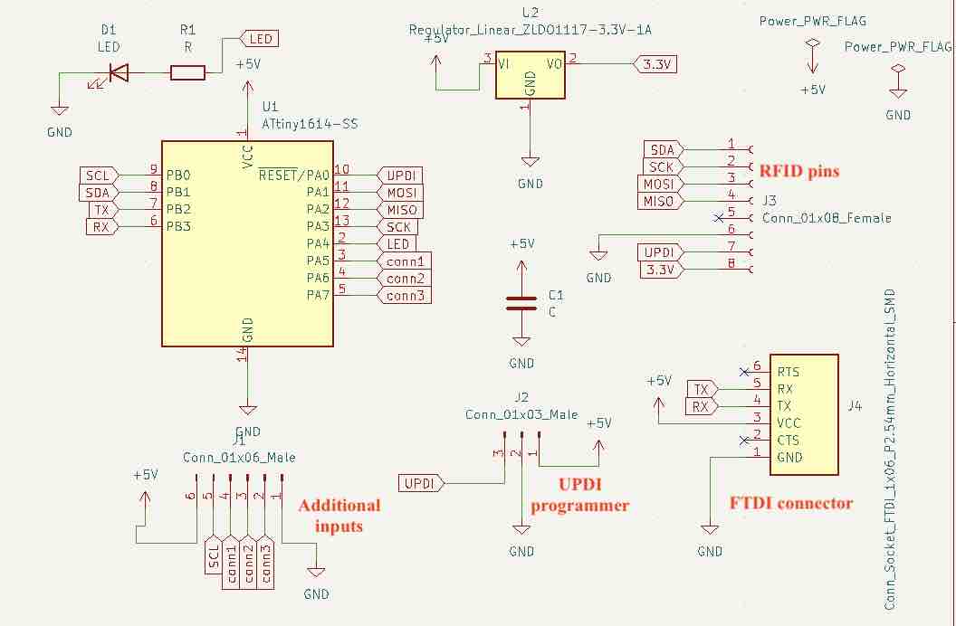
This is the schematic:
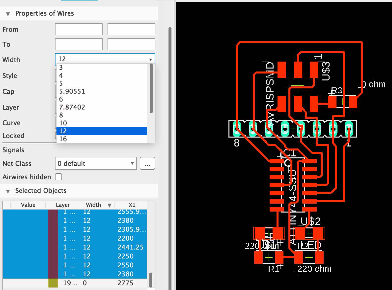
Initially, I had done the traces with the width set to 6. However, while referring back to my notes from electronics productions, I remembered that the width had to be a minimum of 12. I managed to changed all the routing by selecting the whole schematic and then pressing control+shift to selected all the wirings. I also changed two connections for better wiring. Changed the SCK pin on ATTiny pin from 13 to 10 and the SDA pin from 10 to 9.
This is the trace for the board:

Unfortunately, this is all I could do for the week without a lab.
2022
I decided to continue with the RFID and designed a board in eagle with the Attiny1614 as the microcontroller. This is my schematic:
This is the board design:
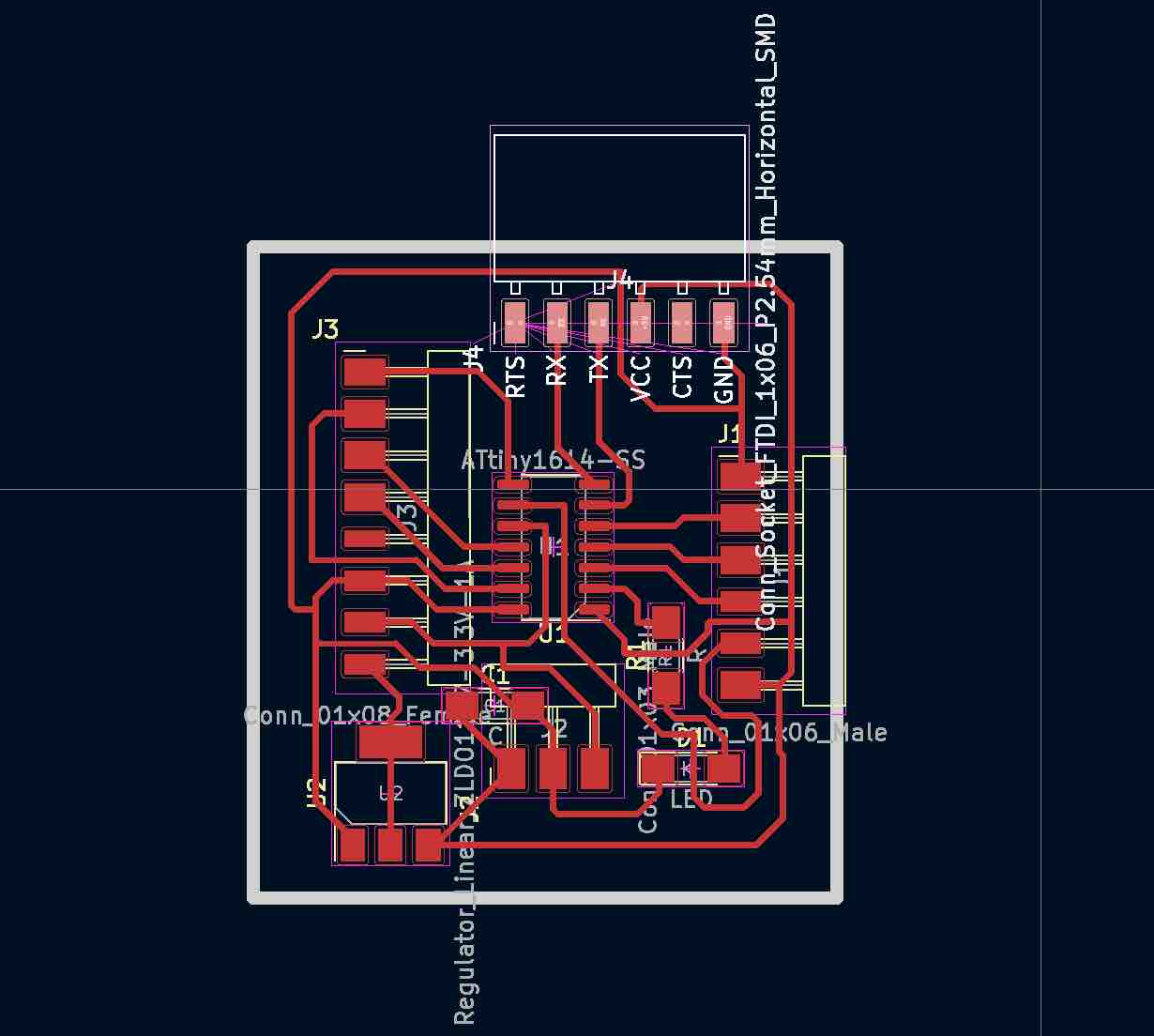
I saved the image and then sent the traces to mill in the SRM-20. However, I realized that some of the traces were too close together and did not mill well.

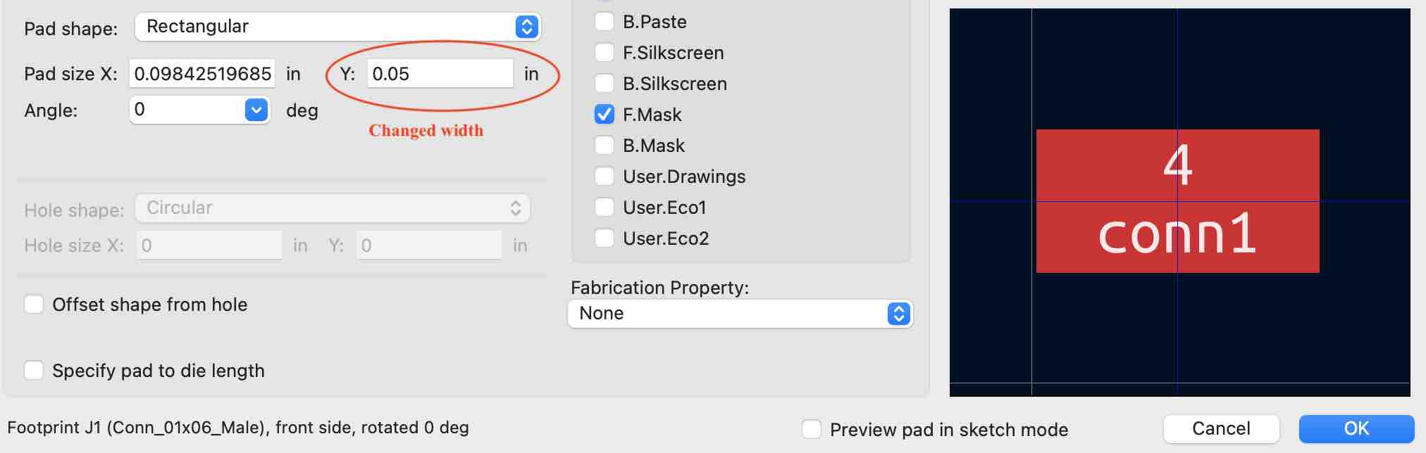
The footprint from the “FTDI header” was smaller than the ones on the “male connectors”. I realized that he one from the FTDI header connections passed through and milled properly. Therefore, I decreased the size of the male connector pads where it hadnt milled to the size of the FTDI connector.
First, I checked the size of the FTDI connector because it had worked for that. You can check by double clicking on any pad.

Next, I checked the size of the pad on the connector where the traces had not passed.

I changed the size of the “Y” to the one from the FTDI pad and saved it.
I milled the board and the traces were milled this time.

When I tried to program the board, there was a problem that said “UPDI initializatiob failed.” I tried to program it again and again to no avail. Suhas sir took one look at my board and said that my connector was touching the traces. I have forgotten to take a picture of my board then but this is what happened with one of my other boards as well:
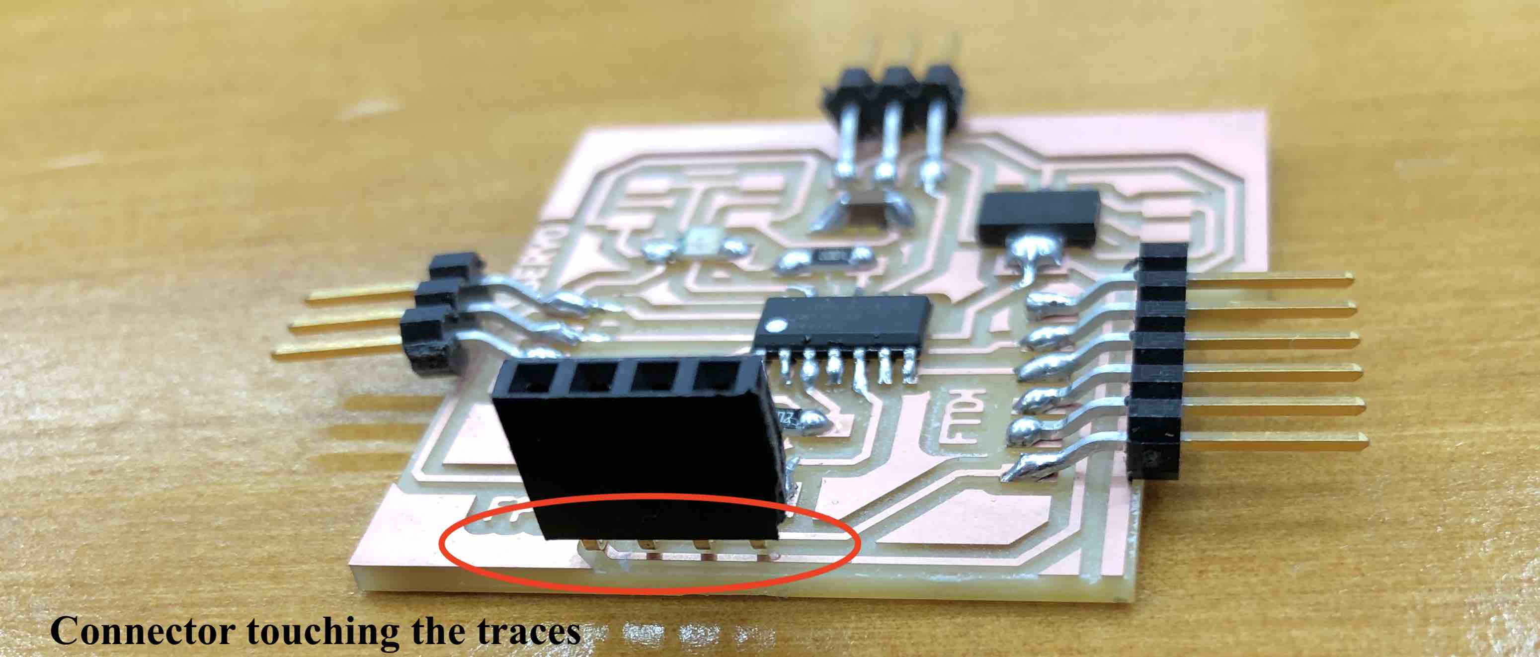
I think this fried my microcontroller.I desoldered the microcontroller using a hot gun and some of the other connectors came out as well. So I soldered on a different connector for the RFID. I left out the connector for the other inputs since it is not required for now. Finally, I changed the number for the reset and SDA pin in the code. I refered to his picture:
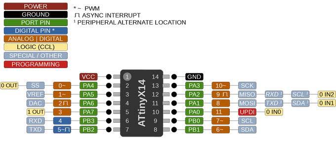
The reset pin and the UPDI pin is the same. It is connected to PA0 which is pin 11 in arduino IDE. The SDA pin is PB1, which is pin 6 on the arduino IDE. I made the changes and uploaded the “Dumpinfo” code through the UPDI programmer first.
Once the code is uploaded I connected the board through the FTDI cable. I had to switch the TX and RX pin for it to work.

Working video: