4. Electronics production
The goal for this week was to make an in-circuit programmer by first milling a PCB, stuffing it with components and then testing it. As a skills building week, we were expected to mill a pre-designed board and get it to work. In the next few weeks we will design our own board and program it to have an input and output. Our group assignment was to characterize the design rules for our PCB production process.
I have milled once in college before but I’ve never used such a small, precise one to mill my own circuit board. I have zero experience with soldering. Therefore, this week was quite the learning experience.
Before starting the class I thought it might be important to define some of the components that we will be working with this week:
PCB (printed circuit board): A PCB is an electronic circuit consisting of thin strips of a conducting material such as copper, which have been etched from a layer fixed to a flat insulating sheet and to which integrated circuits and other components are attached. We will mill this with the Roland SRM-20. Here are some commercial PCBs availible:
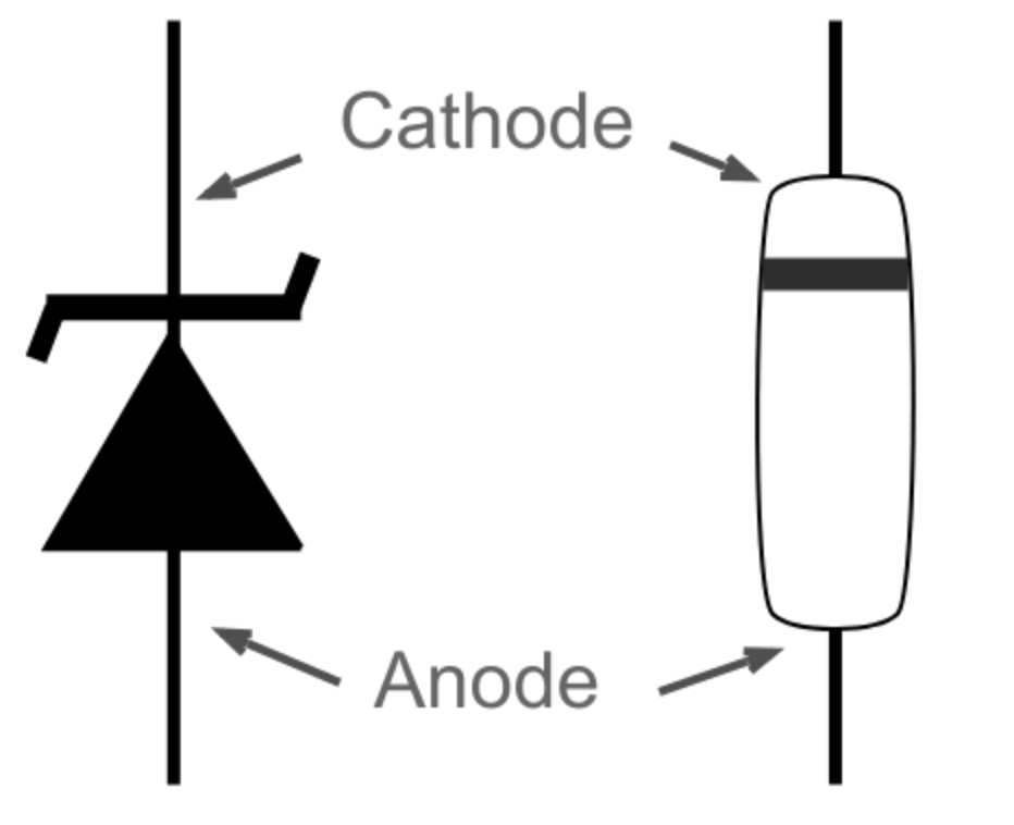
Zener Diode: A Zener diode is a silicon semiconductor device that permits current to flow in either a forward or reverse direction. The diode consists of a special, heavily doped p-n junction, designed to conduct in the reverse direction when a certain specified voltage is reached.
Capacitor: A capacitor is a device that stores electrical energy in an electric field. It is a passive electronic component with two terminals. The effect of a capacitor is known as capacitance. While some capacitance exists between any two electrical conductors in proximity in a circuit, a capacitor is a component designed to add capacitance to a circuit. These are the different symbols of a capacitor in an electrical circuit:

Microcontroller: A microcontroller is a compact integrated circuit designed to govern a specific operation in an embedded system. A typical microcontroller includes a processor, memory and input/output (I/O) peripherals on a single chip.

ISP (in-system programmer): In-system programming (ISP), also called in-circuit serial programming (ICSP), is the ability of some programmable logic devices, microcontrollers, and other embedded devices to be programmed while installed in a complete system, rather than requiring the chip to be programmed prior to installing it into the system.

PCB Fabrication
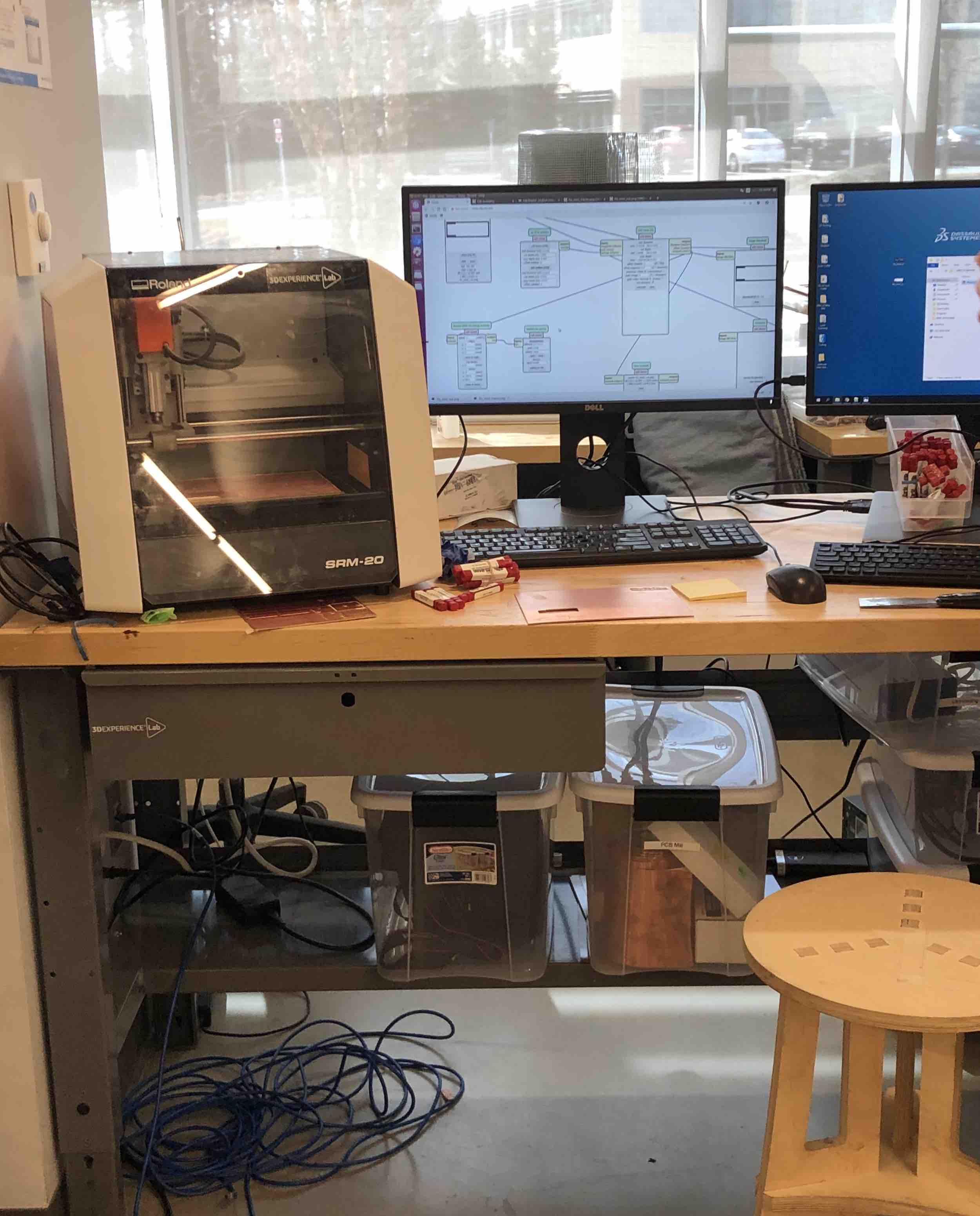
The first step in making an ISP is to mill a PCB. The milling machine that we have in the Dassault Systemes lab is a Roland SRM-20.
I have listed out the steps to milling a PCB:
Step 1: Tape in a sacrificial board to protect the milling-bed. Put double sided tape on the desired stock and stick it on the bed. Press is down so it sticks well.
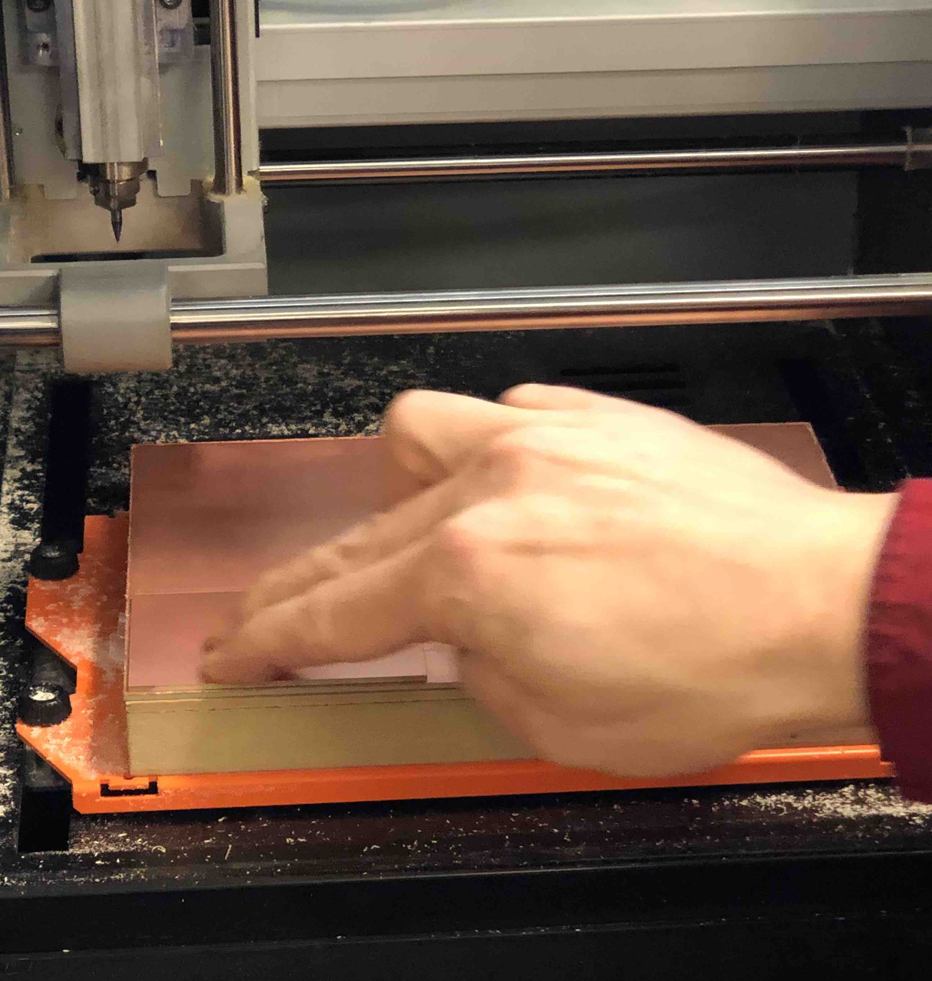
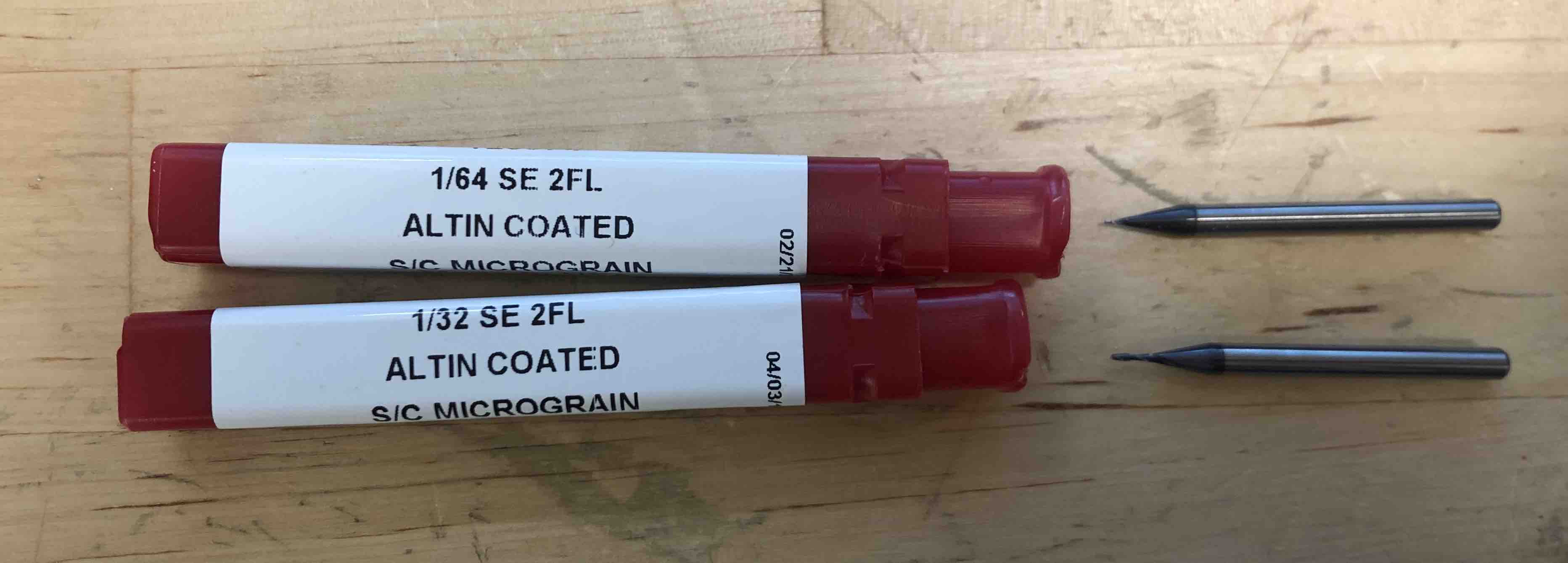
Step 2: Put the desired bit size in the set screw and tighten it with an Allen wrench. We decided to trace the mill first so we put the 1/64 inch bit in.
Step 3: Close the shield and turn on the machine. The light on the machine will blink and it will not turn on if the door is open. Once connected, the machine hums and it is ready to use.
Step 4: Open Mods. Right click mods, go to programs, find machine (PCB png)
Step 5: Set origin to desired spot. Set the Z-position to about 2-3mm above the stock.
Step 6: Untighten the bit and lower it manually till it touches the stock. When tightening the bit again, hold it in place since it tends to ride up.
Step 7: load the desired png file on mods. We loaded the pre-designed png file available in tutorial 5.2 of the Fabacademy tutorials. The black part is what it cuts and the white is what it leaves behind.

Step 8: set pcb tool to trace and the right size.
Step 9: Put in the desired depth and offset number and calculate the path. Once done, hit send file to device

Path of the mill with offset 4:
 Step 10: Milling takes about 10 minutes. Once it is done, vacuum the flakes and visually inspect it.

Step11: change bit to 1/32 inch for cutting.
Step 12: Download the image to cut.
Step 13: repeat step 3 to 7. This is the image used for cutting.

Step 14: Set pcb tool to cut and ensure that the right size bit is selected. Put in the desired depth and offset. Calculate the path and send to device.
Step 15: Once done, vacuum out the flakes and take out the cut part with a spatula.
Step 16: Clean the board with alcohol or water to take out the oil.
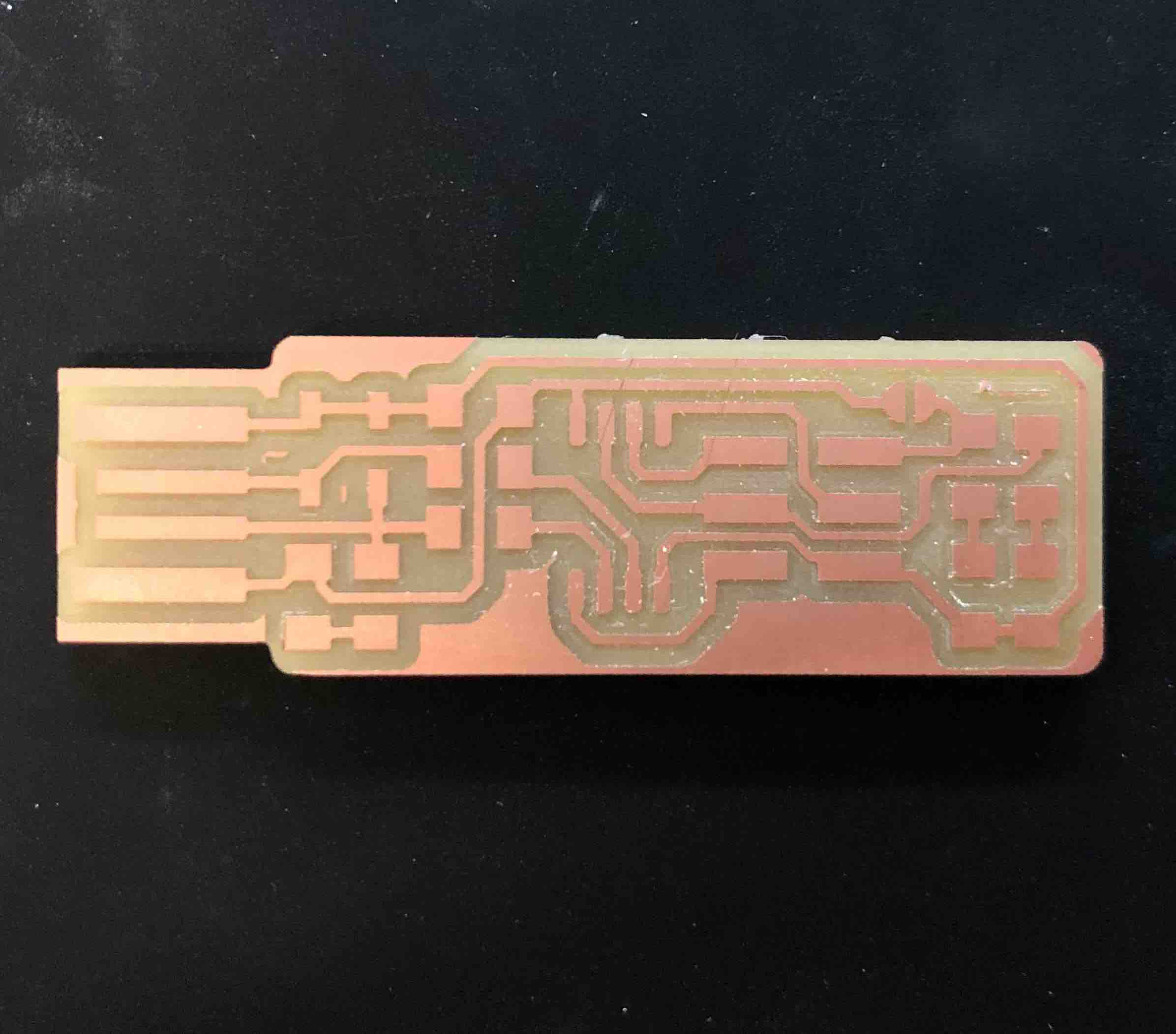
Here is the finished PCB:
Assembling
Soldering
To assemble the components on the board, we obtained the required components first. Here is the list with the components on it:

We started soldering the parts onto the PCB according to the schematic and board image below:

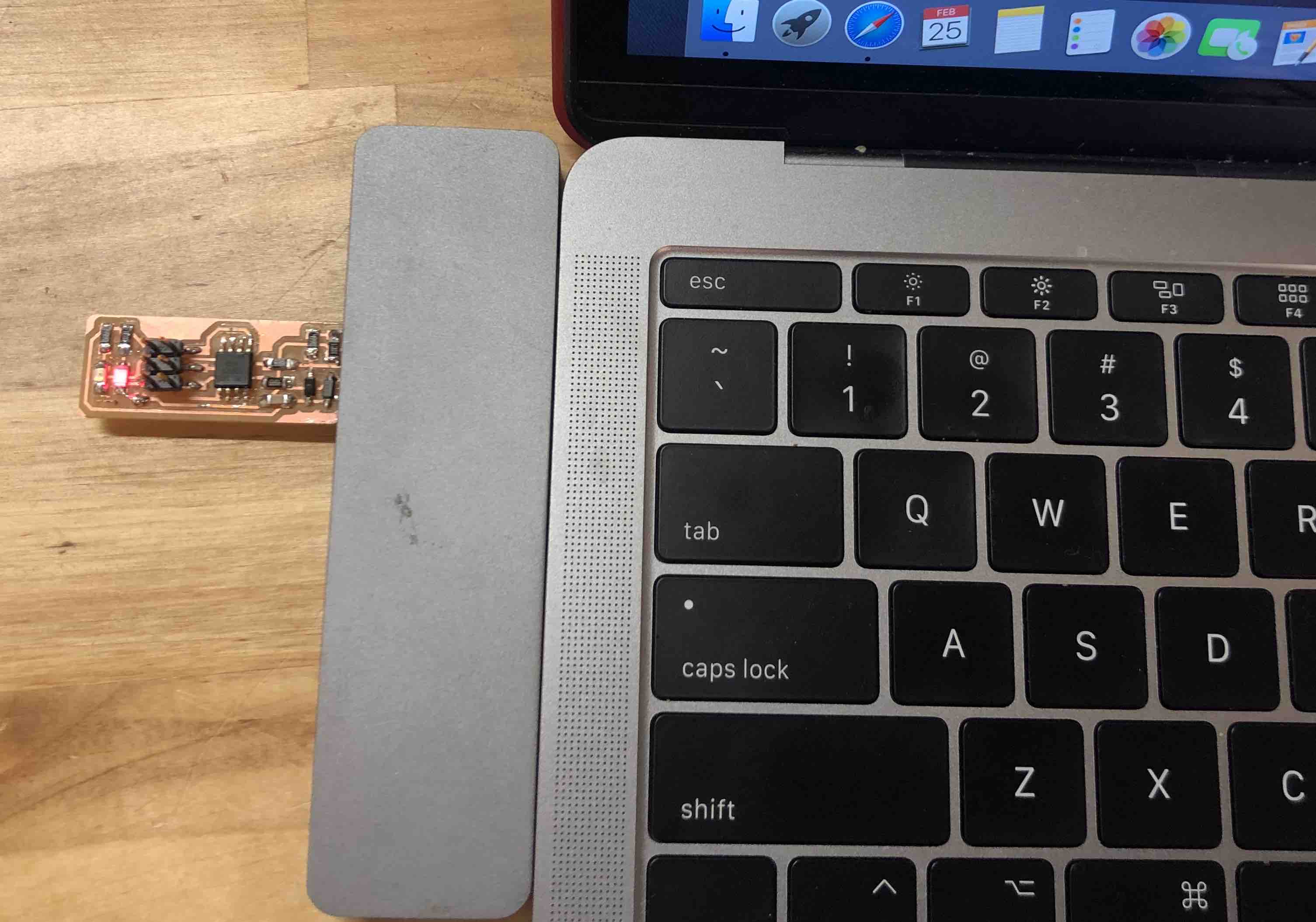
The microcontroller, zener diodes, and the LED lights are orientation sensitive and must be soldered in the right direction. Here is the finished product:

One thing that was really hard with soldering is the size of the components. It was hard to be precise and to be sure that everything was soldered on well. Here is a picture of my palm next to the PCB for size comparision:

Desoldering
Hot-gun: Right before programming my board, I realized that the zener diodes were soldered in the wrong direction. Therefore, I had to take them out and re-solder them onto the board. I did this by holding the component with a tweezer while blowing hot air on the board with a hot gun. When the board gets hot enough, it drops and the component is removed.
Braiding: Braiding is a good method to get extra solder out of the board. It is done by pressing the hot iron on the area where solder needs to be removed with the braid in between. The braid absorbs the solder when the solder gets hot enough.

Programming
This was the most frustrating part of the week. It was really difficult to find out where the problems are. The tutorial in the Fabacademy file was confusing to follow along as well. A multimeter is useful to check for shorts and bad connections. I have listed out the steps taken here:
Step 1: Download and install a Tool chain. The tollchain allows us to get a program written in C launguage and converts it to a .hex file so that the board can read it. I chose crosspack the first time. However, Fab guru Fran suggested avr -gcc since crosspack is outdated.
Go to this website and run the three commands given on there. The commands are listed below:
First, make sure you have xcode command line developer tools installed with
$ xcode-select --install
Then, just run the following to install the latest version:
$ brew tap osx-cross/avr
$ brew install avr-gcc
Step 2: Download the firmware source code and extract the zip file. Open terminal and cd into the source code directory.
Run make. This will build the hex file that will get programmed onto the ATtiny45. When the command completes, you should now have a file called fts_firmware.hex.
Step 3: Update the Makefile for the type of programmer that is going to be used to program the board. The Makefile, by default, assumes that you are going to use a programmer in the usbtiny family. Here are some commonly found AVR programmers: - Small translucent blue programmer: avrisp2 - Large translucent blue programmer: jtag2isp - White box with blue stripe: atmelice A- ny fabbed board with an ATtiny on it: usbtiny
Find the line that says:
PROGRAMMER ?= usbtiny
Change usbtiny to whatever programmer you’re using. The kind of programmer that our instructor, Luciano, had is the avrisp2.
Step 4: Plug the board into a USB port. The red LED light should light up. When I plugged mine in the first time, both the green and the red LED lights lit up and the port started smoking. I quickly disconnected everything and discovered that this was because of a short in my circuit.

I braided out the solder that was shorting my board and tried again. No smoke this time.
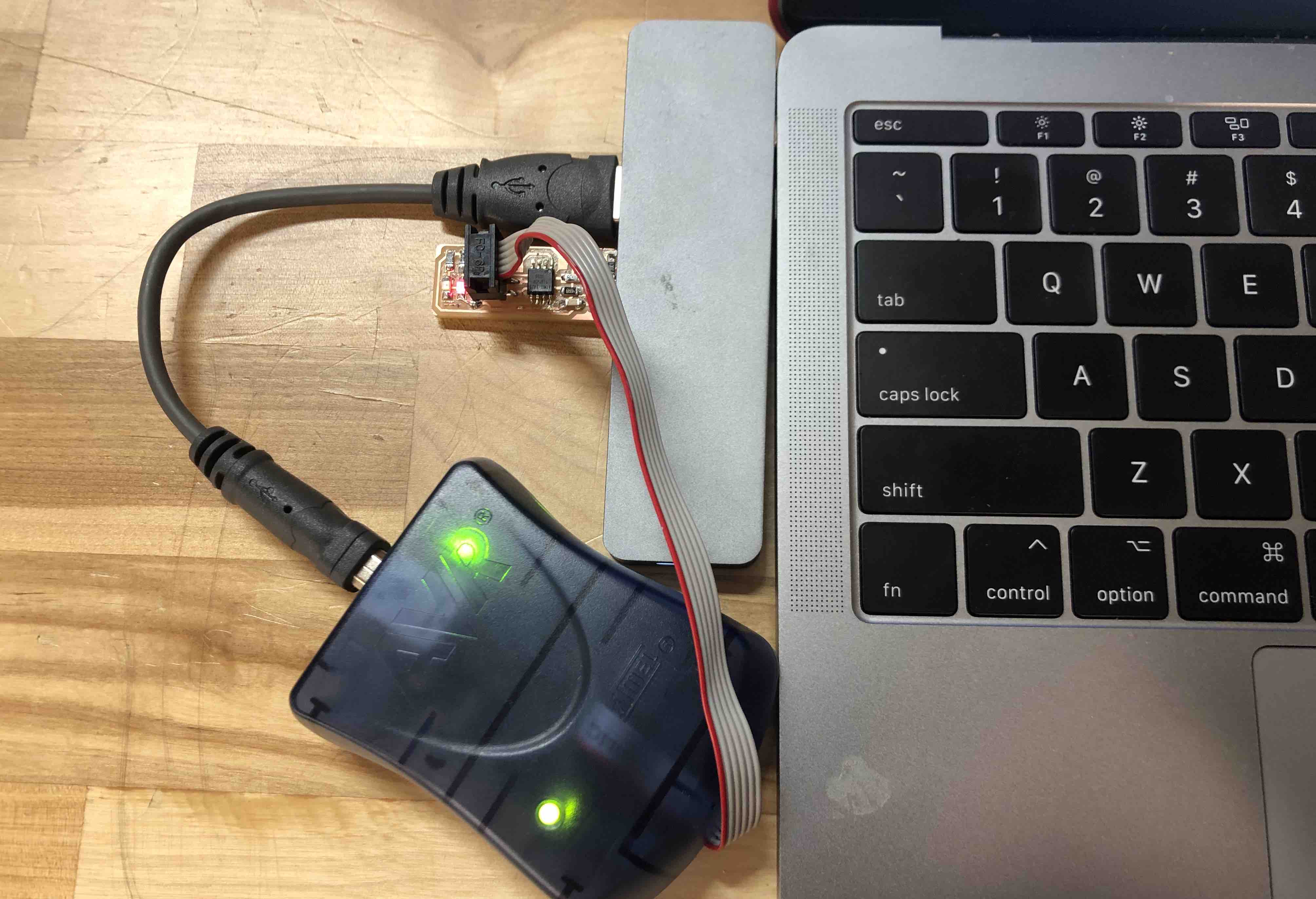
Step 5: Connect the programmer to the ISP header on the board. Remember that the cable is orientation sensitive. Run make flash. This loads the hex file ohto the board.

Once the command runs successfully, the light in the programmer will turn green. This means that the board is programmed.
Step 6: Run make fuses command. This sets the configurations in the microcontroller. The board can be reprogrammed up to this point.

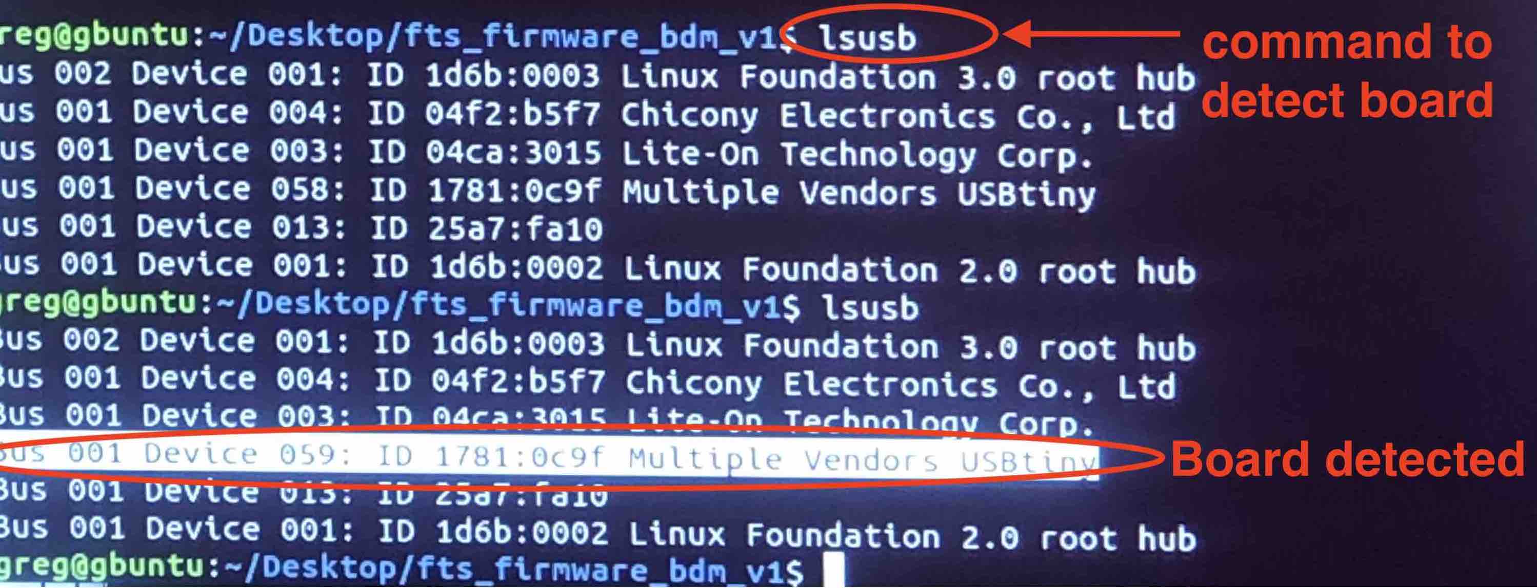
The next step in the process, according to the tutorial, is to check if my laptop reads the board. It did not. I tried this step numerous times, with a bridge, without a bridge. I even started the whole process again, milling, soldering and programming, just to get stuck here again.
I tried my first board on my instructor Greg’s Linux computer and it was able to read the board.
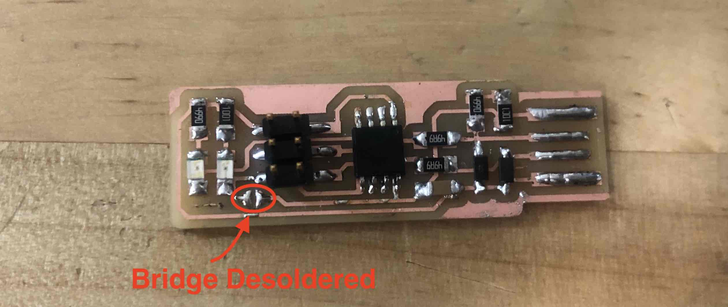
Step 7: Run make rstdisbl command. This will blow the reset fuse. Once this is done, avrdude will not be able to talk to the chip through the ISP reader. The board can never be reprogrammed again. This command protects the board from being reprogrammed to do something else.
Step 8: Desolder the bridge connection. The programmee is now a programmer!
*If the bridge is soldered on, the isp can give power to the board it is programming. If the bridge is desoldered, the power to the board being programmed has to be provided separately.
Testing the FabISP
To ensure that the FabISP works as a programmer, I programmed the board that I had made during the output devices week with the FabISP. To load the program, I used Arduino IDE. Under the tools tab, ensure to change the programmer to “USBtinyISP.”

I uploaded the program to my output devices board and it worked! Here is the video:
Group Assignment
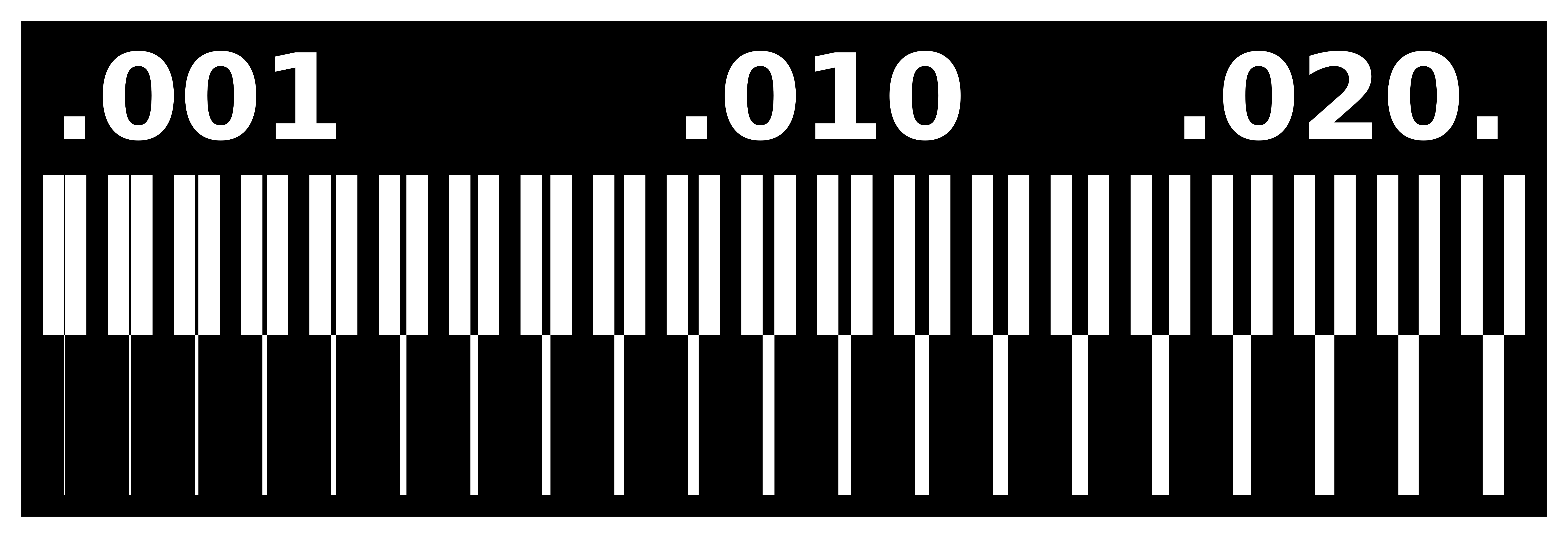
The group assignment for this week was to characterize the design rules for our PCB production process. To do this, we traced the image below using a 1/64 inch bit and a 1/32 inch bit.
 Here is the result:

From the image above, you can see that the 1/64 inch bit trace was more precise than the 1/32 inch bit trace. Also, the 1/64 inch bit did not cut all the way through the copper. This is probably because the bit was not lowered enough before tracing or because the depth in the setting was too shallow.
The images also shows that the 1/32 inch bit causes fraying in parts that are smaller in length.

2022 work
Group assignment
For the group assignment, we first downloaded the png images from the fabacademy website.
For the traces:
For the interior:

We ran the traces using a 1/64 inch bit. Here are the results:
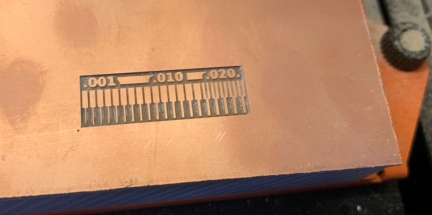

You can see that the trace width and the space is only visible properly in the 0.020 range. This is because 1/64” is 0.015 and 0.02 is the only range that is bigger than that. Therefore, for our future circuit boards, we have to stay in this range.
Connecting to MODS and the SRM-20
Since MODs was not connected directly to the SRM-20, we had to make a few changes to get it to work.
Step 1: Open up the MIT MODS website. On the website, you have to right click and then follow this path:
Programs -> open server program -> Roland -> SRM 20 -> PCB png
This will bring up the following page. We now need to upload a PNG file to trace and then one to cut. Once this is done, we can calculate the toolpath.
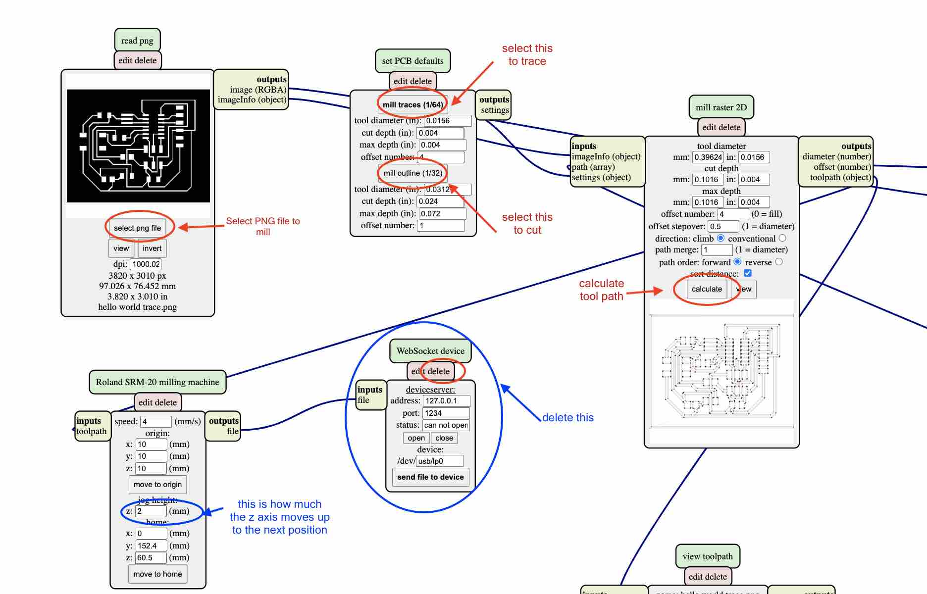
Step 3: Since the milling machine is not connected directly to Mods, we need to delete the websocket device and add another path to save the file. We do this by following this path:
right click -> modules -> open server module -> file (save).
This will add the save file option on mods. We now need to connect the file under “Roland SRM-20 milling machine” to the file under “save file.” Now, when calcute is clicked, it will automatically save the .rml file. This file then needs to be uploaded on the Roland software.

Step 4: Now that we have the .rml file, we have to open up the roland software and upload it there. On the sofware, we set the X,Y and Z orgins and then start running the machine.

Assessment Guide
Linked to the group assignment page (Done on this page)
Documented how you made (mill, stuff, solder) the board
Documented that your board is functional
Explained any problems and how you fixed them
Included a ‘hero shot’ of your board