Electronics Design, Production, Testing and Integration
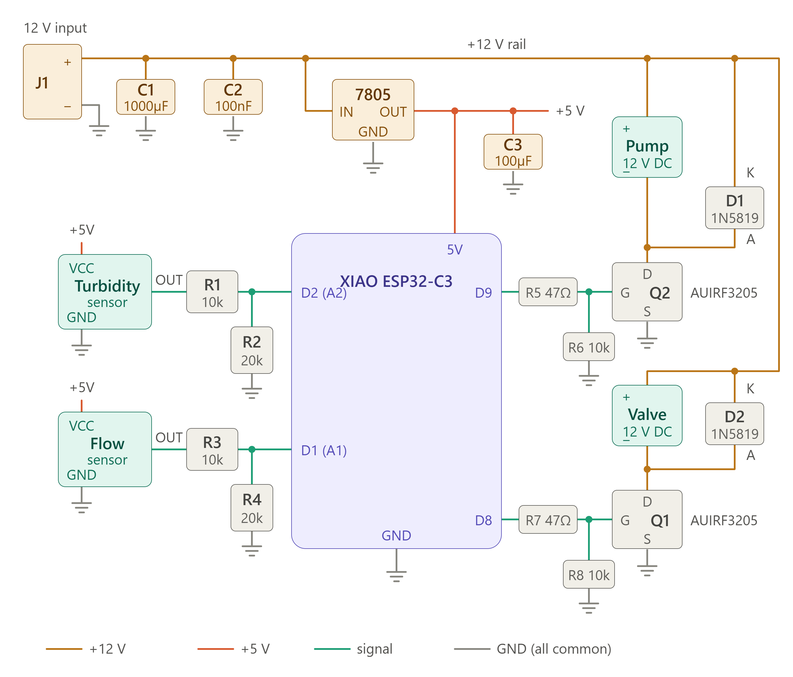
| Component | Function |
|---|---|
| J1 | 12 V DC power input |
| C1 | Bulk reservoir capacitor; smooths voltage ripple |
| C2 | Decoupling capacitor; filters high-frequency noise |
| 7805 | Regulator; steps 12 V down to 5 V |
| C3 | Smooths the 5 V power rail |
| XIAO MCU | Reads sensors and drives the MOSFETs |
| Turbidity | Water clarity sensor with analog output |
| R1 | Upper voltage-divider resistor; scales 5 V to 3.3 V |
| R2 | Lower voltage-divider resistor; connects the divider to GND |
| Flow | Flow sensor with pulse output |
| R3 | Upper voltage-divider resistor; scales 5 V to 3.3 V |
| R4 | Lower voltage-divider resistor; connects the divider to GND |
| R5 | Limits current into the Q2 gate |
| R6 | Pull-down resistor; keeps Q2 off during boot |
| Q2 | Low-side MOSFET switch for the pump |
| Pump | 12 V pump that pushes water through the filter |
| D1 | Flyback diode; absorbs voltage spikes from the pump |
| R7 | Limits current into the Q1 gate |
| R8 | Pull-down resistor; keeps Q1 off during boot |
| Q1 | Low-side MOSFET switch for the valve |
| Valve | 12 V solenoid valve that releases clean water |
| D2 | Flyback diode; absorbs voltage spikes from the solenoid valve |
1. Initial Circuit Design and Programming
Main Controller
For the initial design, I used the Seeed Studio XIAO ESP32-C3 (SMD) as the main controller.
Output devices - Solenoid valve - Water pump - 16 × 2 I2C LCD - LEDs
Input devices - Flow rate sensor - Turbidity sensor
Initial PCB Design Using KiCad
I used KiCad to design the circuit schematic and PCB layout. For PCB production, I used the Roland SRM-20 milling machine, a 40° V-bit for milling the traces and a 0.8 mm end mill for cutting the board outline.
Schematic Design
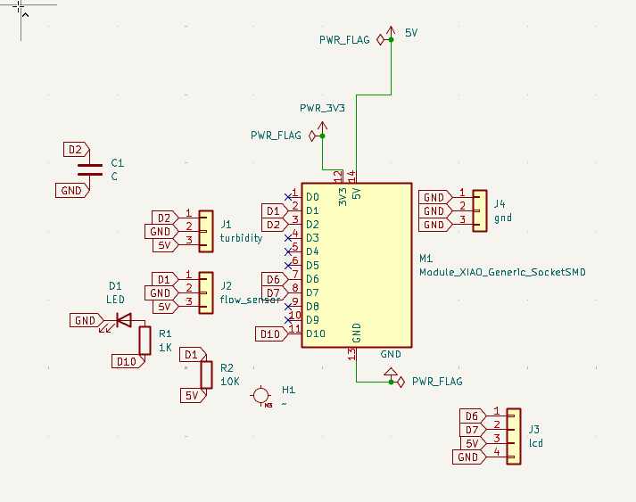
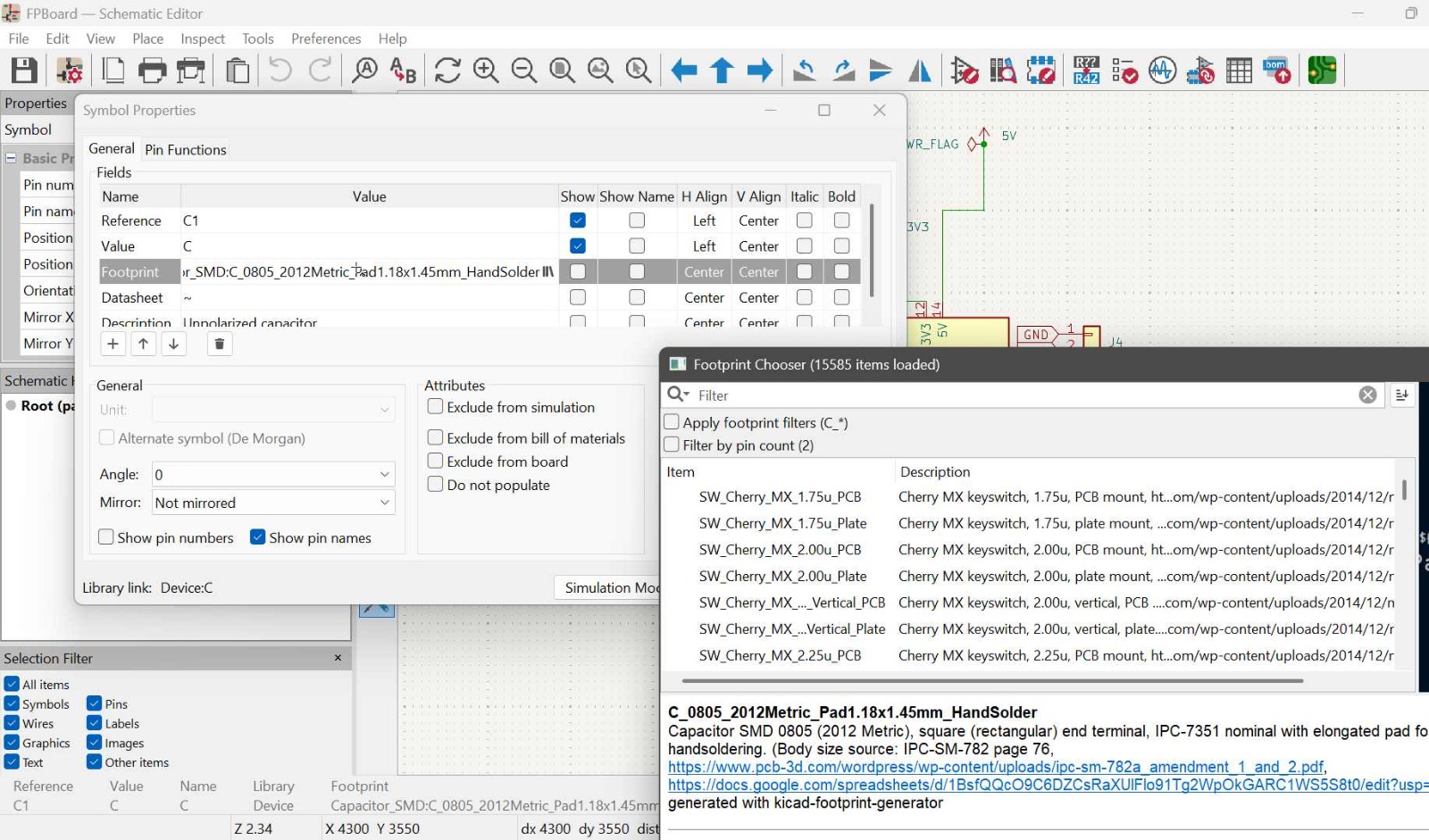
To assign footprints to the components, I first added them from the KiCad library using the component selection tool. I then opened the component properties and searched for the correct footprint.
To identify the correct footprints, I referred to the component models and datasheets available online.
PCB Layout
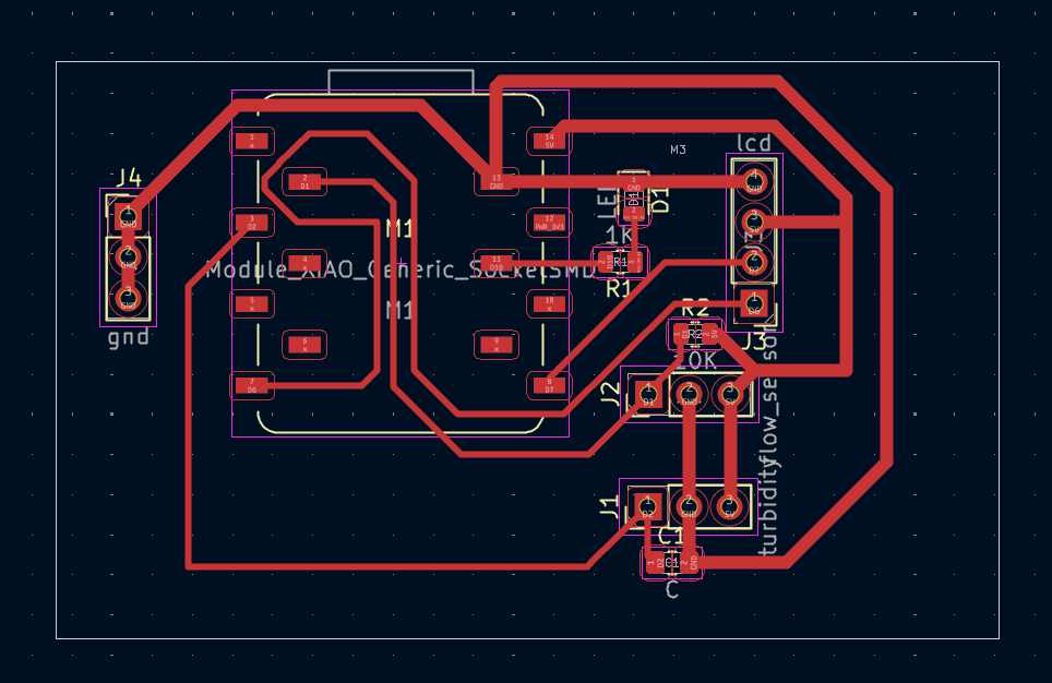
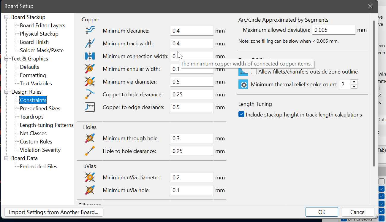
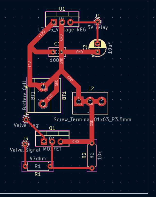
Under Board Setup, I configured the minimum track width and clearance requirements.
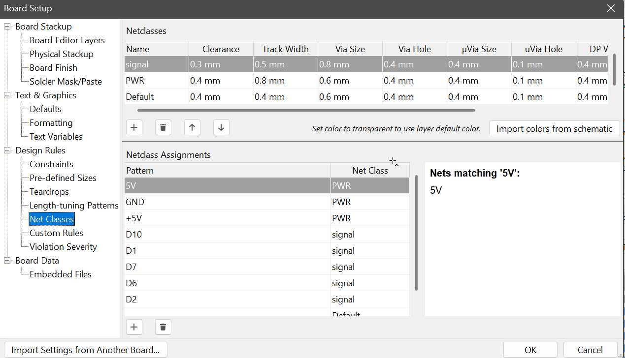
Since power traces carry more current than signal traces, I assigned different net classes to ensure that the power and signal tracks had appropriate widths.
Exporting Files and Generating Toolpaths
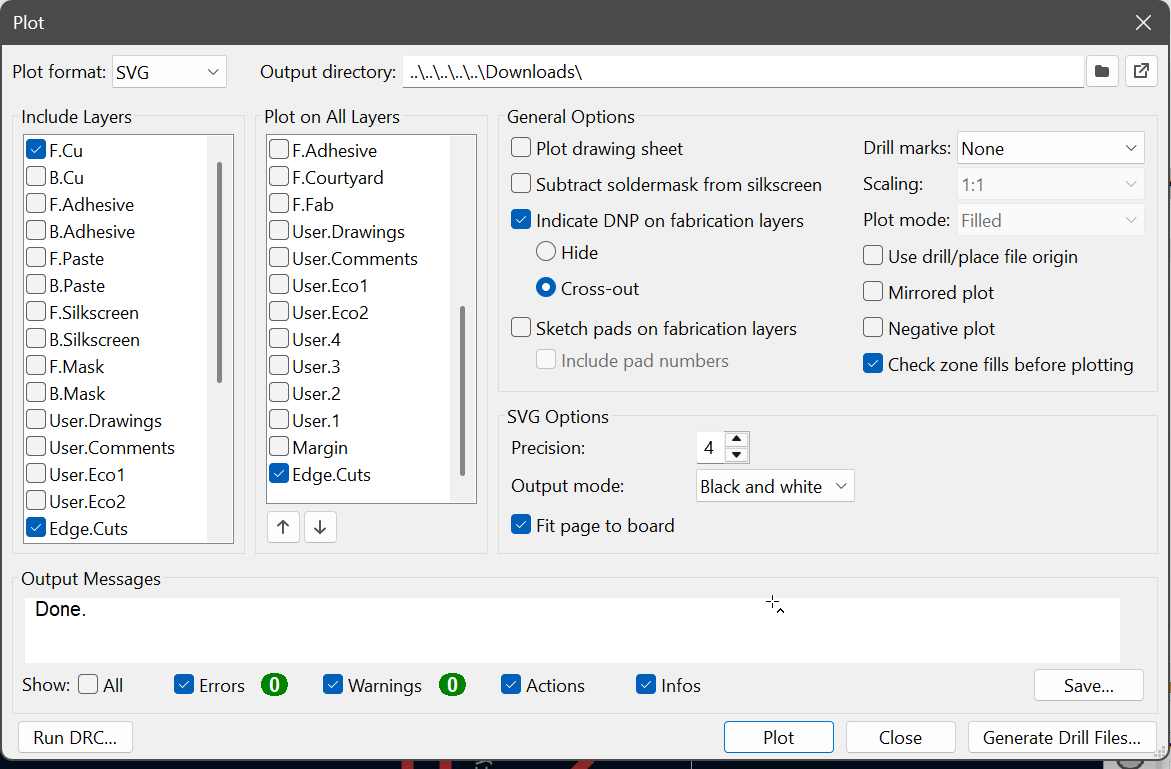
During the plotting process, I exported SVG files for the front copper layer (F.Cu) and board edge cuts. I also selected the option to fill the page to the board to make the process easier when generating toolpaths in MODS.
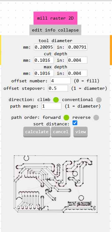
In MODS, I selected the Roland SRM-20 machine and the 40° V-bit. I then calculated the cutting depth, maximum depth and tool diameter before adjusting the settings.
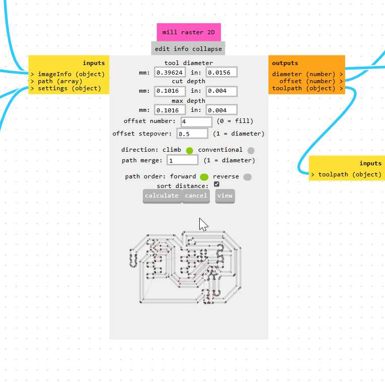
I also set the X and Y coordinates to zero instead of using the default values.
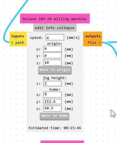
The milling and cutting process is documented in my Electronic Production week.
Power Board Design
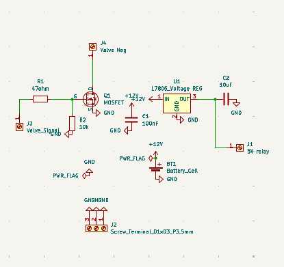
I also designed a separate power board to manage the power supply and switching circuit.
Schematic design
3D view
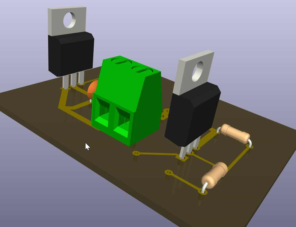
Voltage Regulator
An LM7805 voltage regulator was included to convert the 12V supply to a regulated 5V output. I also used a 10µF capacitor at the regulator output to improve voltage stability and reduce fluctuations.
MOSFET Switching Circuit
An N-channel MOSFET was used as an electronic switch for controlling the 12V solenoid valve.
The gate was connected to the controller output through a 47Ω resistor, while a 10kΩ pull-down resistor was connected between the gate and ground. This keeps the MOSFET OFF when there is no control signal.
The drain was connected to the negative terminal of the load, while the source was connected to ground. When a control signal was applied, the MOSFET switched ON and allowed current to flow through the load.
Solenoid Valve and Pump Connections
The positive terminal of the 12V solenoid valve was connected to the 12V supply, while its negative terminal was connected to the MOSFET drain.
The 12V water pump was also connected in parallel with the solenoid valve in the initial circuit design. Both loads could therefore be controlled through the same MOSFET switching circuit.
Power Filtering
A 100nF capacitor was connected across the main 12V supply line to reduce electrical noise and improve the stability of the power circuit.
Programming
I developed the firmware for the Seeed Studio XIAO ESP32-C3 to combine turbidity monitoring, flow-rate measurement, LCD display and MQTT communication.
The program included:
- Reading turbidity values from the sensor.
- Measuring water flow using the YF-S201 flow sensor.
- Calculating the flow rate and total water volume.
- Displaying readings on a 16 × 2 I2C LCD.
- Connecting to Wi-Fi.
- Publishing water quality and flow information to an MQTT broker.
- Controlling the valve and pump through the MOSFET switching circuit using active-low logic.
I used ChatGPT to assist in generating and combining the initial Arduino code. I provided the following prompt:
Develop a single Arduino sketch for the Seeed Studio XIAO ESP32 that combines the existing turbidity monitoring system with a YF-S201 flow sensor and MQTT communication.

The system should read turbidity from A2, measure flow rate and total volume using the flow sensor on D2, display turbidity status and flow information on a 16×2 I2C LCD (SDA = D6, SCL = D7), connect to Wi-Fi and publish flow rate, total liters, turbidity percentage, and water quality status to an MQTT broker every second.

The valve/MOSFET connected to D10 should be controlled using active-low logic based on the turbidity level.
The initial firmware and its complete implementation are retained in this section of my project documentation.
2. Change of Design
After working on the initial design, I realised that I needed a more compact system with a single power source capable of supplying the controller and the output devices, including the water pump and solenoid valve.
I also identified some challenges with the initial electronics enclosure, wiring arrangement and PCB layout. The wiring and cut board were not as neat as I wanted, so I decided to redesign the electronics rather than continue with the existing arrangement.
I therefore developed a new circuit schematic and PCB layout using EasyEDA.
This allowed me to reorganise the components, improve the circuit arrangement and work towards a more compact design.
New Circuit Schematic
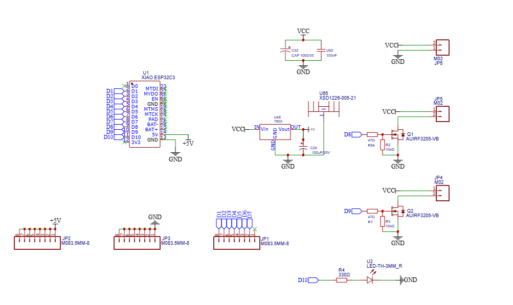
The new schematic included the required components for the controller, power management and output switching.
Components Required
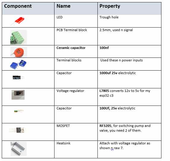
Testing the Circuit Before PCB Production
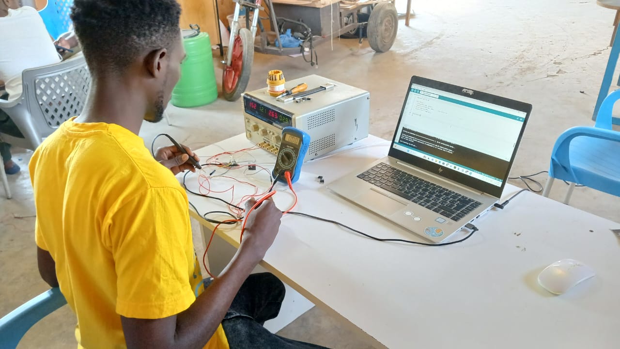
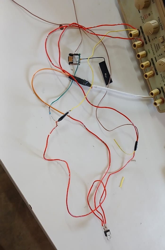
Before producing the new PCB, I assembled and tested the circuit externally using connecting wires.
This allowed me to check the connections and confirm that the circuit could operate before transferring the design to the PCB.
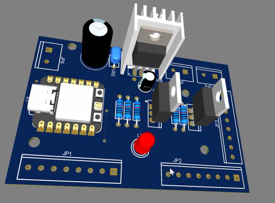
3D view
After completing the schematic, I viewed on in 3D view to check the arrangement of the components.
3. PCB Production Using EasyEDA and MODS
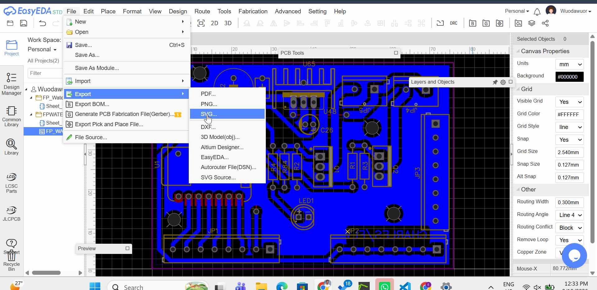
Exporting the Design
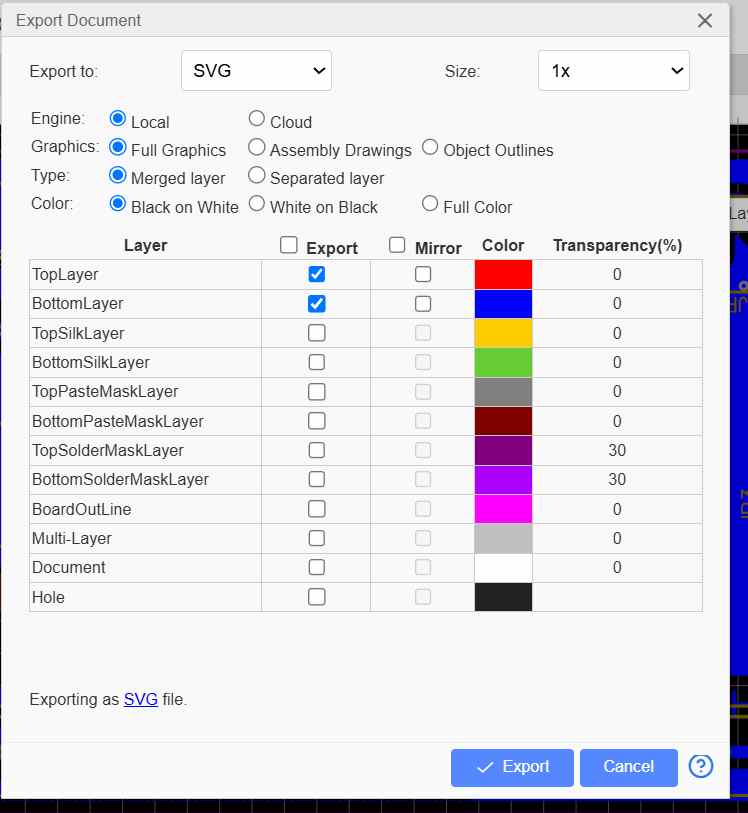
I used EasyEDA to prepare the PCB design for production. I exported the SVG files for the top and bottom layers.
During the export process, I selected the required copper layers and checked the SVG properties before generating the toolpaths.
Generating Toolpaths Using MODS
I used MODS Project to generate the toolpaths for the PCB milling process.
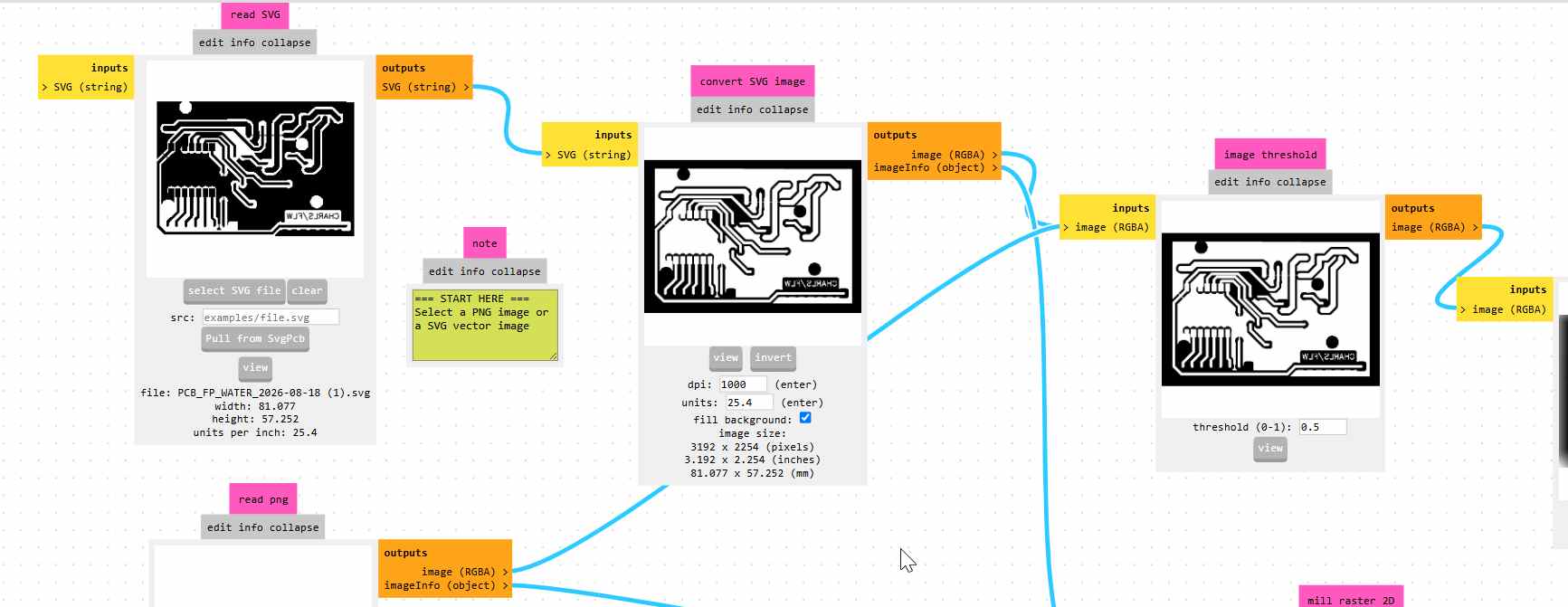
I selected a 40° V-bit for milling the copper traces.
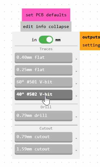
I then checked the toolpath properties before proceeding with production.
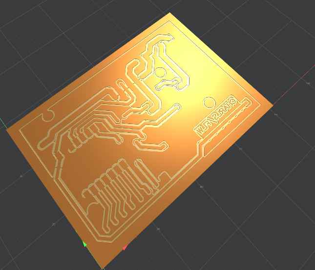
3D View of the PCB
4. Electronics Testing and Troubleshooting
Challenge Encountered During Hardware Testing
After assembling the control PCB, I uploaded the firmware to the Seeed Studio XIAO ESP32-C3 to test the pump and solenoid valve control.
The microcontroller started correctly, the LCD displayed the startup message, and the program executed without errors. However, neither the pump nor the solenoid valve responded to the control signal.
Instead of assuming that the PCB or software was faulty, I decided to troubleshoot the circuit step by step.
Step 1: Verify the ESP32 Output
I first confirmed that the ESP32 was producing the expected output signal.
I uploaded a simple test program to toggle GPIO D8 continuously between HIGH and LOW.
Using a digital multimeter, I measured the voltage between D8 and ground.
| Test | Result |
|---|---|
| D8 → GND | 0–3.4V alternating |
This confirmed that the microcontroller was producing the expected output signal.
Step 2: Verify the Loads
To confirm that the problem was not caused by the pump or solenoid valve, I tested both devices independently using the 12V power supply.
Pump test
I connected the pump directly to the 12V supply.
Result: The pump operated normally.
Solenoid valve test
I connected the solenoid valve directly to the 12V supply.
Result: The valve actuated correctly with an audible click.
This confirmed that both output devices were working.
Step 3: Verify the MOSFET Driver Circuit
I then focused on the MOSFET switching circuit.
The following measurements were taken while the ESP32 output was toggling.
| Measurement | Result |
|---|---|
| D8 → GND | 0–3.4V |
| Source → GND | 0V |
| Drain → GND | 12V |
| Pump (+) → GND | 12V |
| Pump (−) → GND | 12V |
Since the drain remained at 12V, the MOSFET was not switching the load as expected.
Step 4: Check PCB Connections
The next step was to inspect the connections around the MOSFET.
I performed continuity tests between:
- ESP32 D8 and the gate resistor.
- Gate resistor and MOSFET gate.
- MOSFET gate and pull-down resistor.
- Pull-down resistor and ground.
The PCB traces were electrically continuous, so I proceeded to check the actual component values.
Step 5: Isolate the Circuit from the PCB
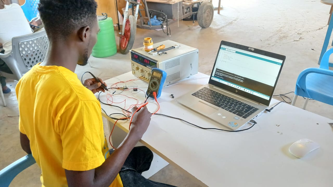
At this stage, I wanted to determine whether the problem was caused by the circuit design itself or by the assembled PCB.
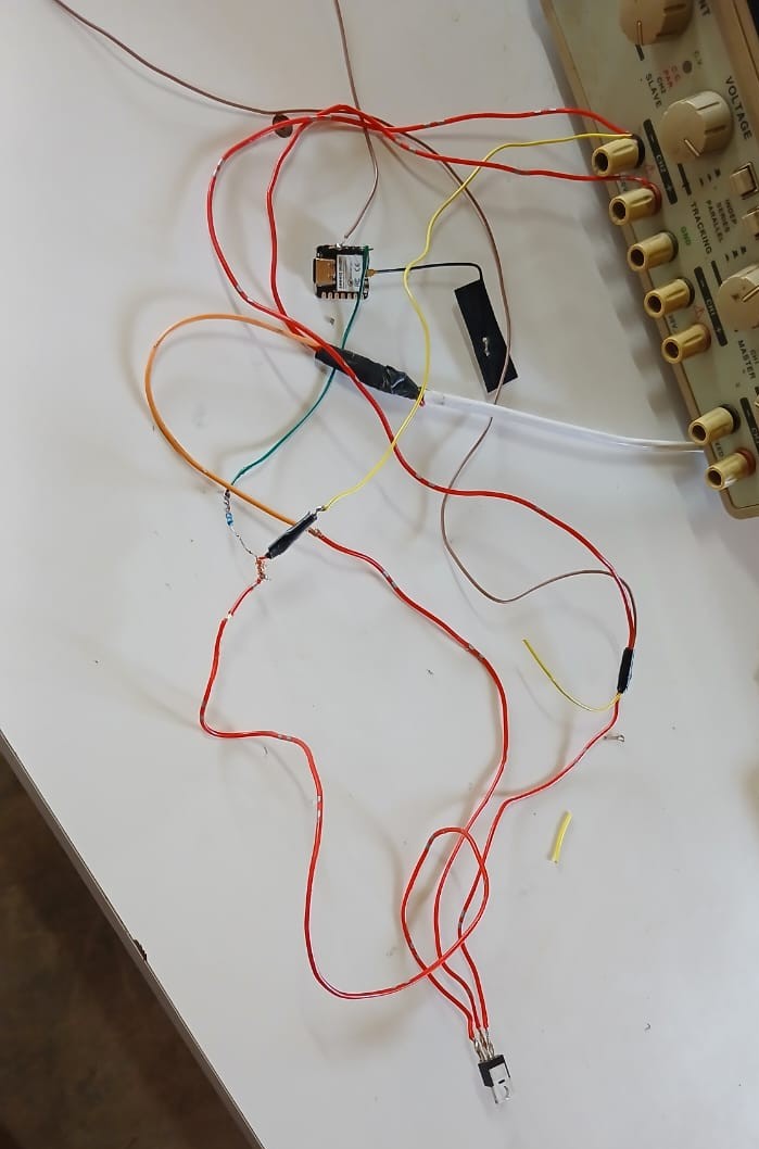
To investigate, I rebuilt the MOSFET driver circuit outside the PCB using connecting wires.
The test circuit consisted of:
- Seeed Studio XIAO ESP32-C3.
- IRLB4132 logic-level MOSFET.
- 47Ω gate resistor.
- 10kΩ gate pull-down resistor.
- 12V DC power supply.
- 12V DC pump.
- Solenoid valve.
I used the same firmware that had been uploaded to the PCB without making any software changes.
Observations
When the circuit was connected externally:
- The pump switched ON and OFF correctly.
- The solenoid valve actuated correctly.
- The MOSFET responded to the ESP32 control signal.
- The gate voltage alternated between approximately 0V and 3.3V.
Conclusion
Since the same circuit operated correctly when assembled externally, I concluded that the schematic design, firmware, ESP32, MOSFET, pump and solenoid valve were functioning properly.
The problem was therefore related to the assembled PCB rather than the circuit design itself.
Step 6: Inspect the Assembled PCB
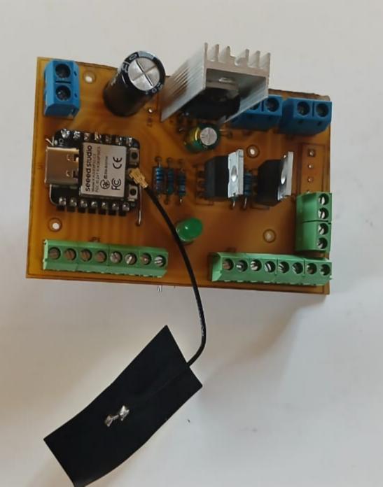
After confirming that the circuit worked externally, I returned to the PCB and carefully inspected every component against the schematic.
I checked:
- MOSFET orientation.
- Continuity of PCB traces.
- Solder joints.
- Resistor values in the gate driver circuit.
During this inspection, I discovered that I had assembled the PCB with an incorrect resistor value.
The design required a 47Ω gate resistor and a 10kΩ pull-down resistor. However, I had mistakenly installed a 470Ω resistor in place of the 47Ω resistor, and one of the required resistors had also been omitted during assembly.
I replaced the incorrect resistor with the correct 47Ω resistor and installed the missing resistor.
After making these changes, the MOSFET driver operated as expected.
Final Verification
I tested the PCB again using the same firmware.
This time:
- The pump switched ON and OFF correctly.
- The solenoid valve operated correctly.
- The MOSFET responded reliably to the ESP32 GPIO output.
- The complete control PCB functioned without further modifications.
This troubleshooting process helped me understand the importance of checking component values, PCB connections and hardware behaviour before assuming that a circuit design or firmware is faulty.
5. Electronic Enclosure Box Design and Production
After completing the electronics, I returned to the enclosure design.
My initial enclosure needed improvement because I wanted the PCB to fit properly without depending on hot glue. I also wanted a stronger and more organised arrangement for mounting the electronics.
I therefore redesigned the enclosure to accommodate the circuit board, improve wire management and provide proper screw mounting points.
Enclosure Redesign
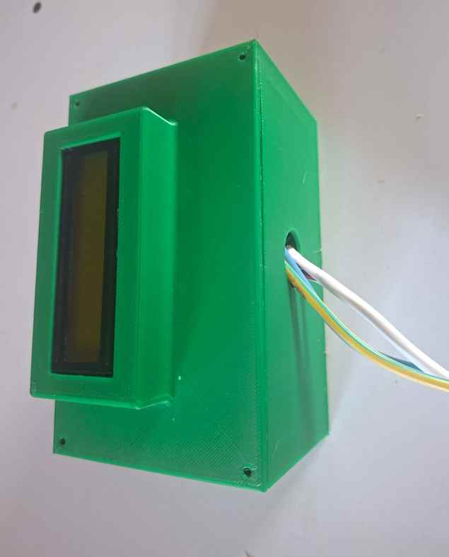
I modified the enclosure to:
- Fit the PCB properly.
- Provide screw holes for mounting the entire enclosure onto a surface.
- Provide mounting points for securing the PCB inside the box.
- Allow the lid to close securely using screws.
- Improve cable management and reduce unnecessary openings.
PCB Fitting
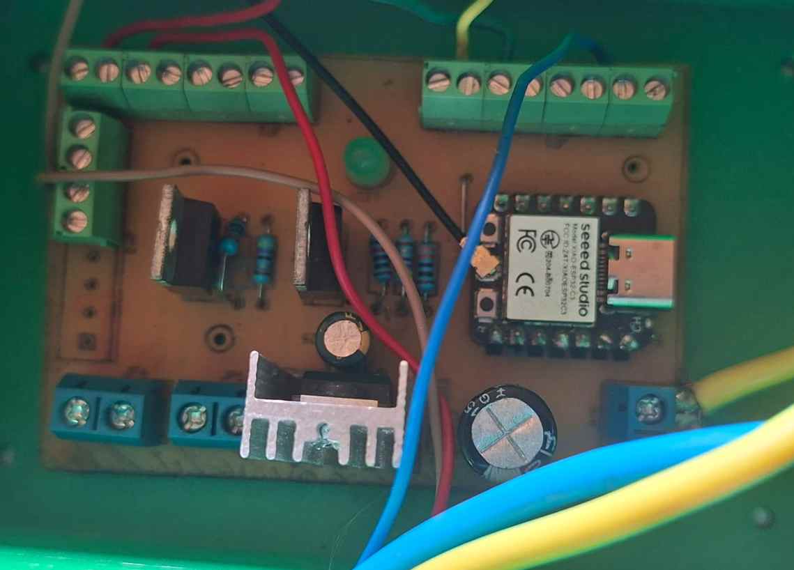
I checked the dimensions and positioning of the PCB to ensure that it fitted properly inside the enclosure.
I also wanted to use a single opening for all the wires instead of creating multiple holes. This would help reduce unnecessary openings that could expose the internal electronics to water leakage.
Printing the Enclosure
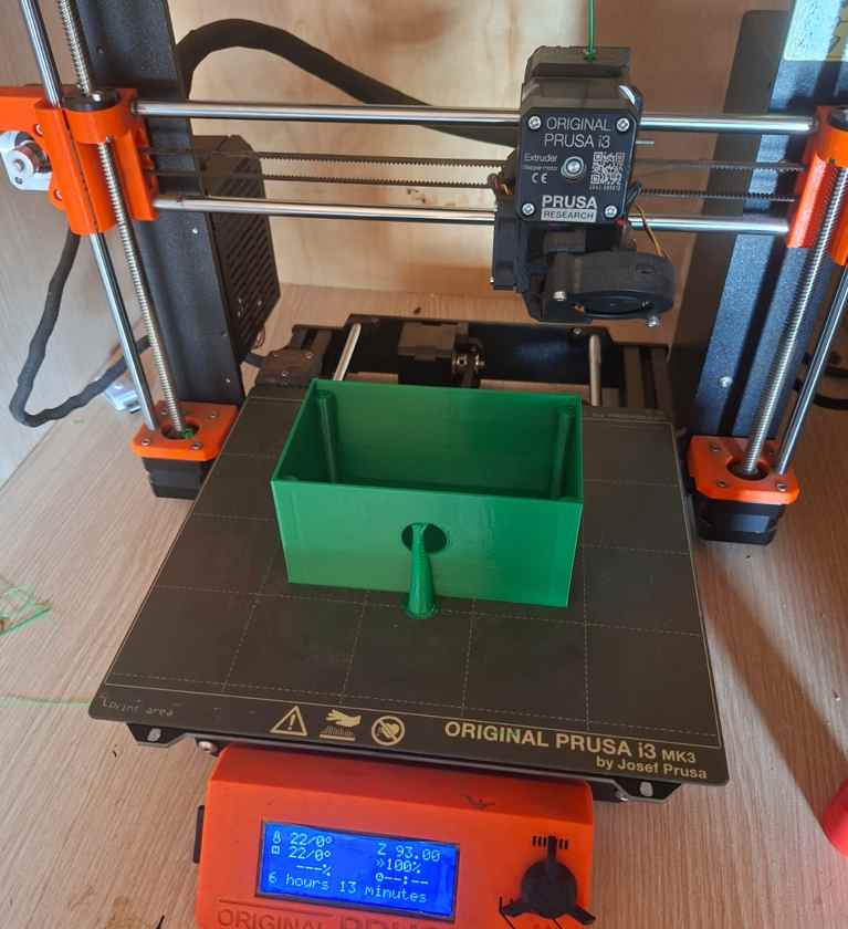
After completing the modifications, I produced the redesigned enclosure.
The lid was designed to fit using screws, allowing the electronics to remain securely enclosed. I also tested the assembly to check that the lid remained in place when the enclosure was dropped.
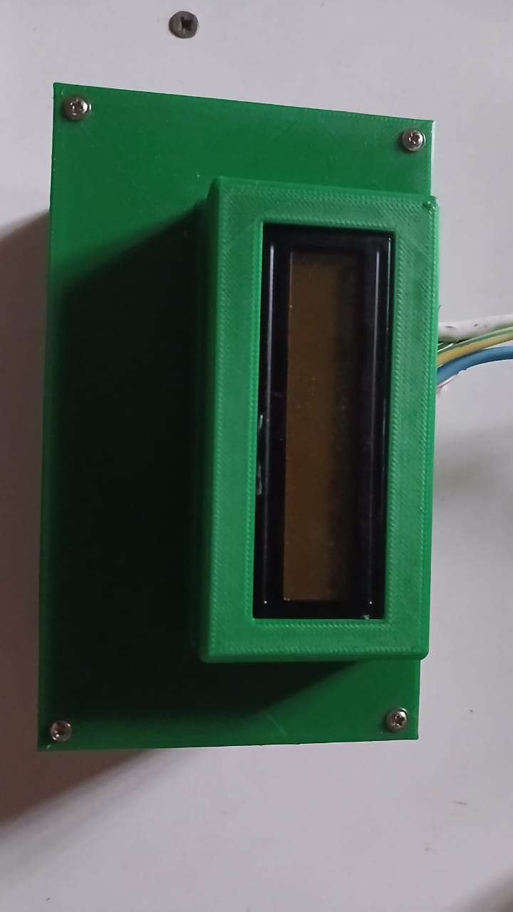
Internal Mounting
I secured the controller PCB inside the enclosure using screws instead of hot glue.
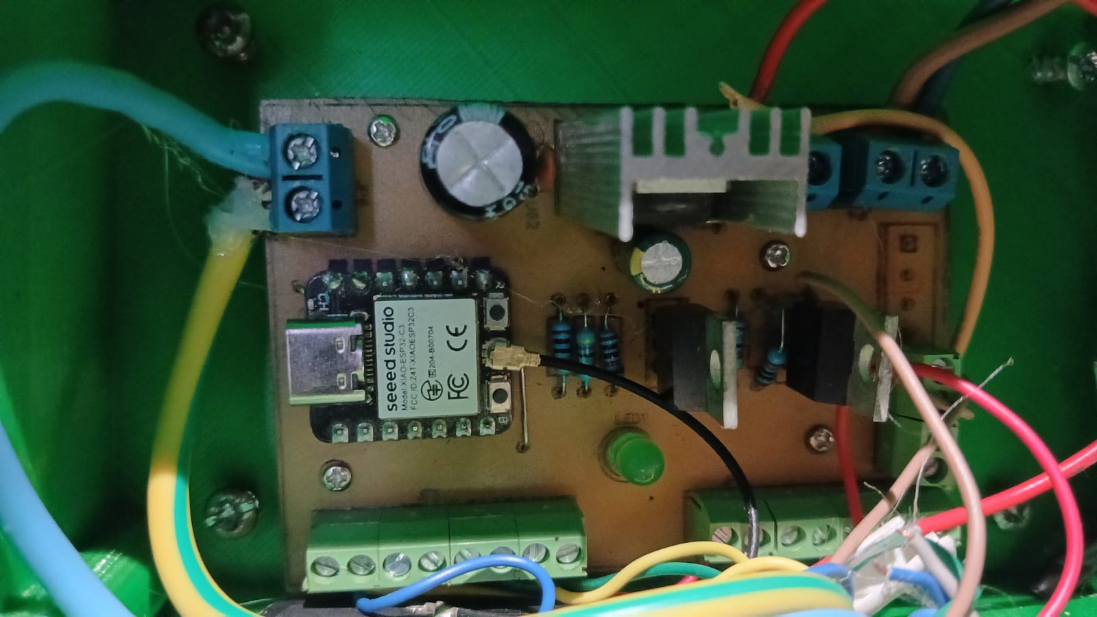
This made the assembly neater and easier to maintain because the board can be removed when repairs or modifications are needed.
I then secured the components using screws.
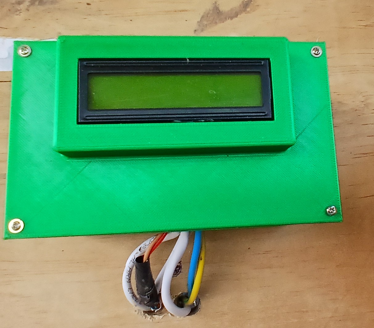
6. Final Product
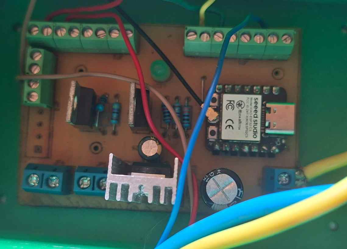
The redesigned electronics and enclosure provide a more organised arrangement for the water monitoring and control system.
The redesign also gave me an opportunity to improve my PCB design, hardware troubleshooting, component selection, 3D enclosure design and mechanical integration skills.
8. Project Files
PCB STEP File
SVG Files
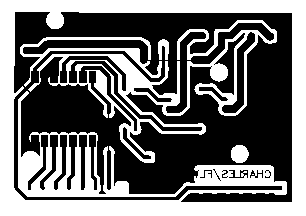
Gerber Files
Additional PCB Files
Initial PCB Files
The following files were generated for the initial board:
- Edge cut Gerber: gerber file
- Edge cut SVG: edgecut SVG
- Front copper Gerber: front copper gerber
- Front copper SVG: frnt copper svg
- Front copper RML: front copper rml
- Edge cut RML: edge cut rml

