Appearance
WEEK 8 – Electronics Production
Assignments
Group Assignment
- Characterize the design rules for your in-house PCB production process
- Submit a PCB design to a board house
Individual Assignment
- Make and test an embedded microcontroller system that you designed
- Extra credit: make it with another process
Group Work
Our group work is accessible HERE (add the link)
Individual Work - PCB Design & Production
This week, I have machined a circuit board using the Roland MDX-40, a compact desktop CNC machine. As a first trial and test, I have decided to design and produce an extension board for the XIAO ESP32-C3 that I might be able to use for my final project.
PCB Design Process
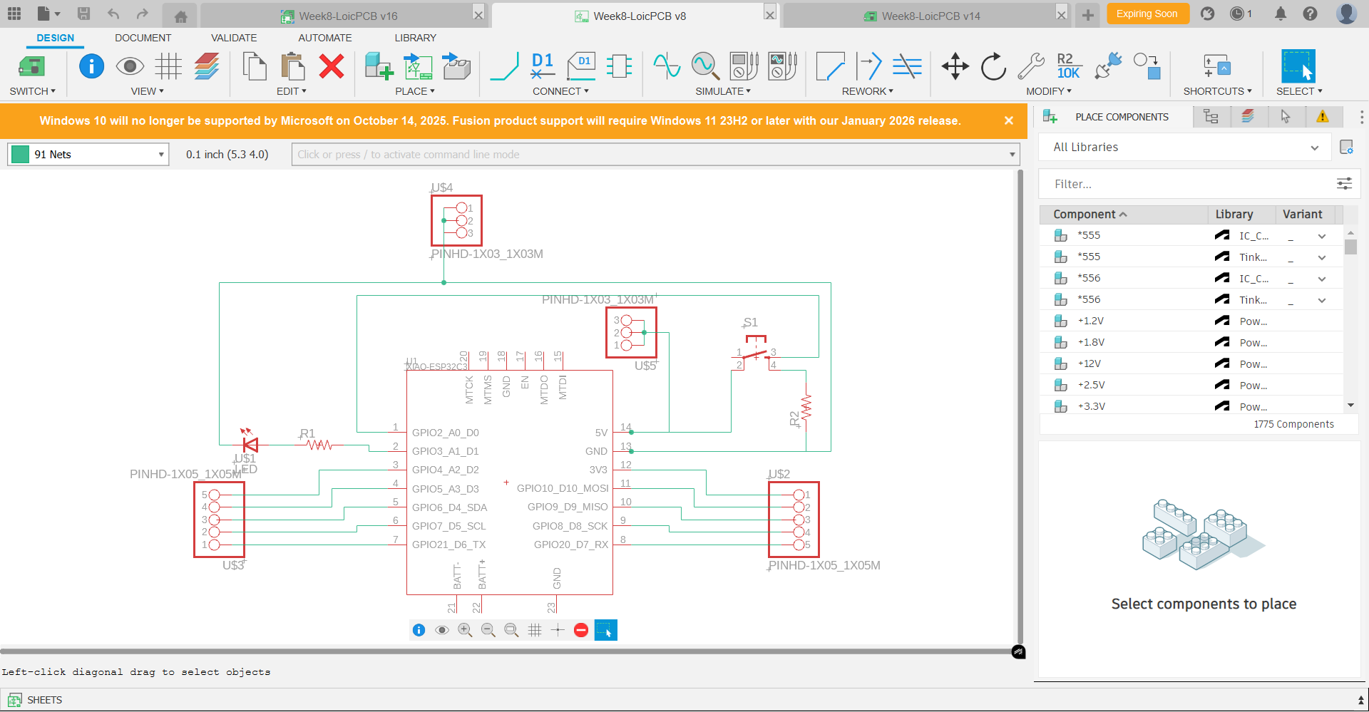
Using Fusion 360, I have designed the following PCB:
Step 1: Schematic of the extension board. 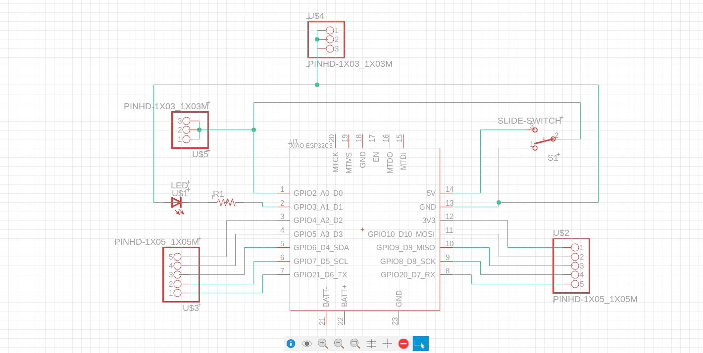
Note: The LED is wrongly oriented in the schematic above. This has been corrected in my final PCB design and production for this week. Scroll-down to the last section of this webpage, "ROUND SIX for the Production of my PCB" to visualise the correct final schematic. (ROUND 5 was supposed to be the improved final version, but I made a mistake with a wrong wiring of the Switch and connecting the Resistor to D0 pin instead of the GND pin) 😦 😦 😦
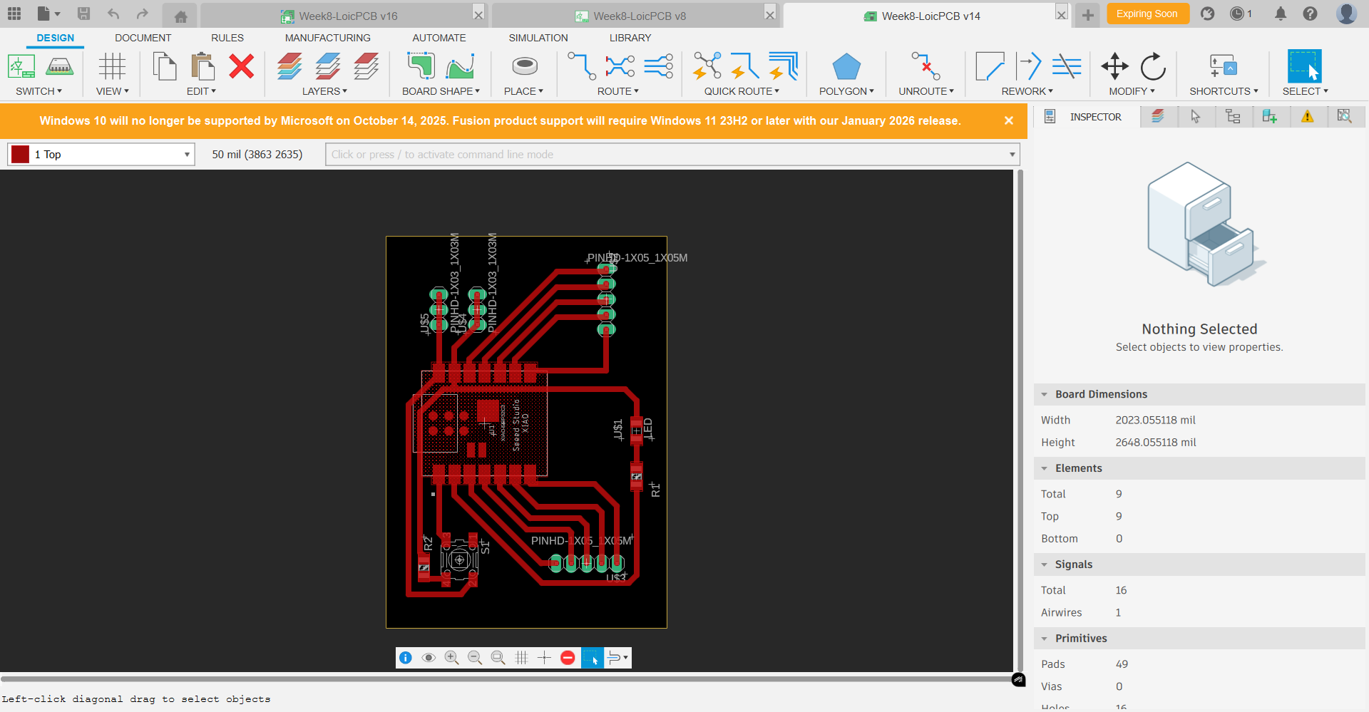
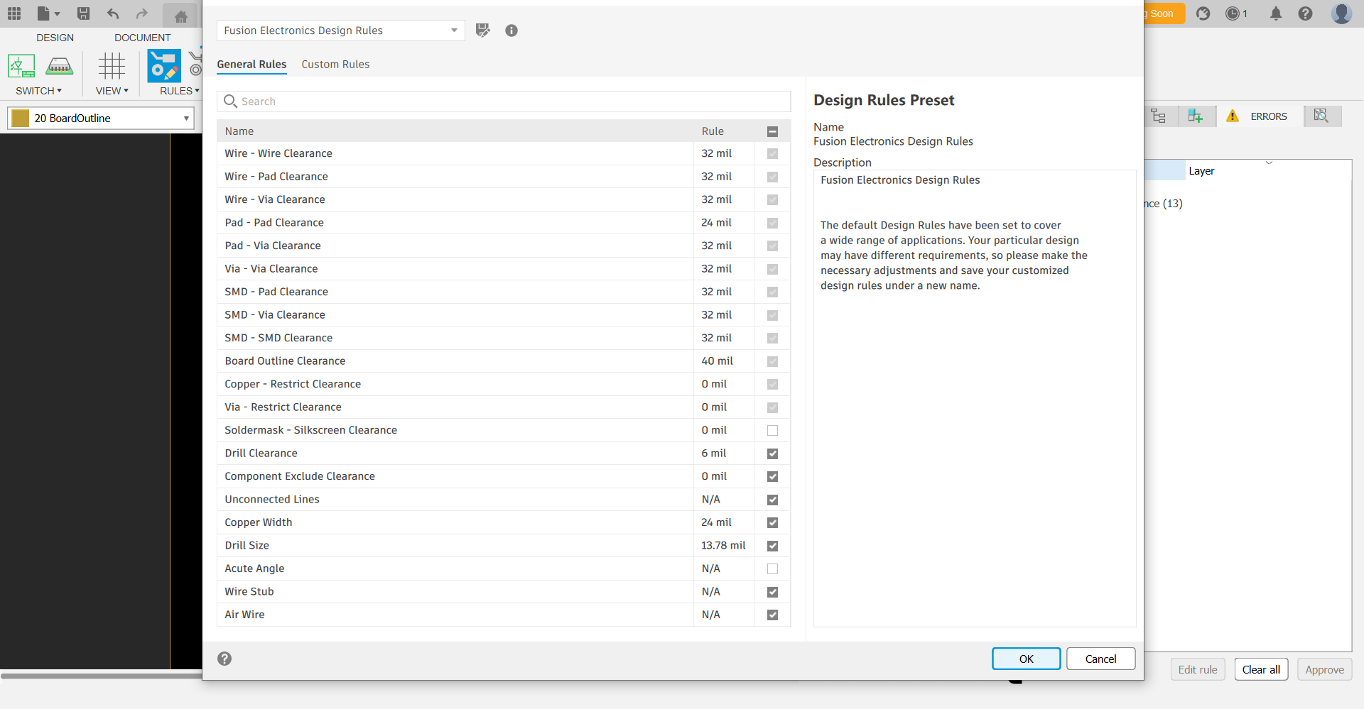
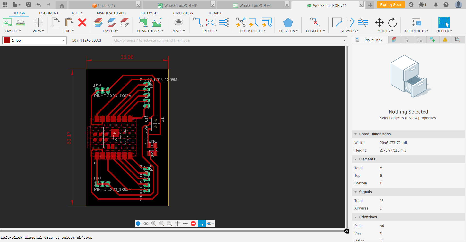
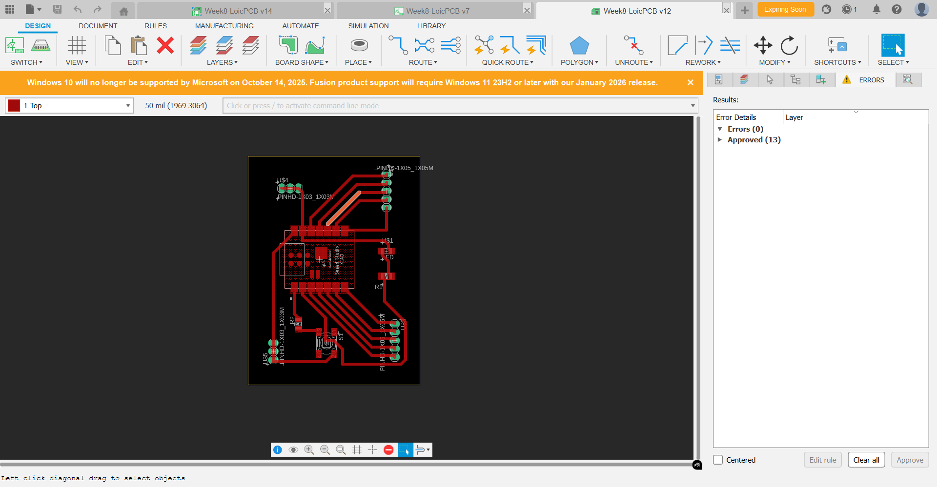
Step 2: Switch to 2D PCB mode, review the Design Rules settings, and refine the layout of the components. 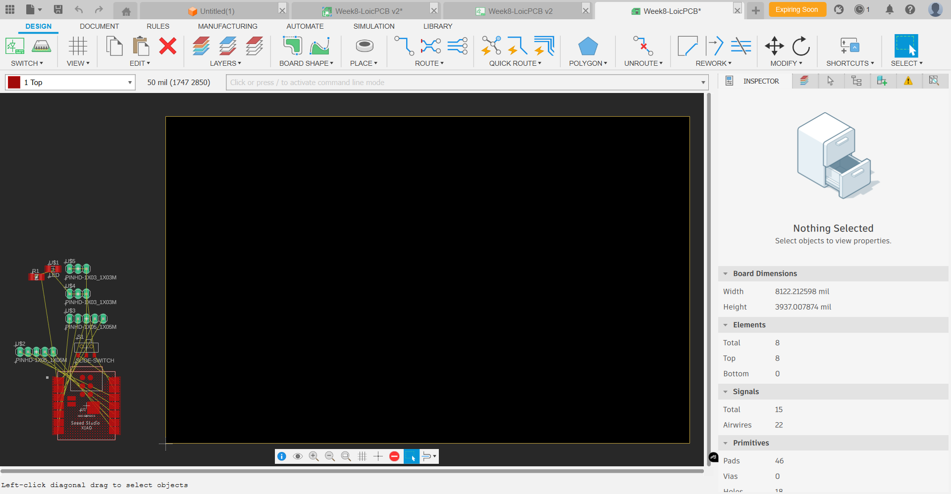
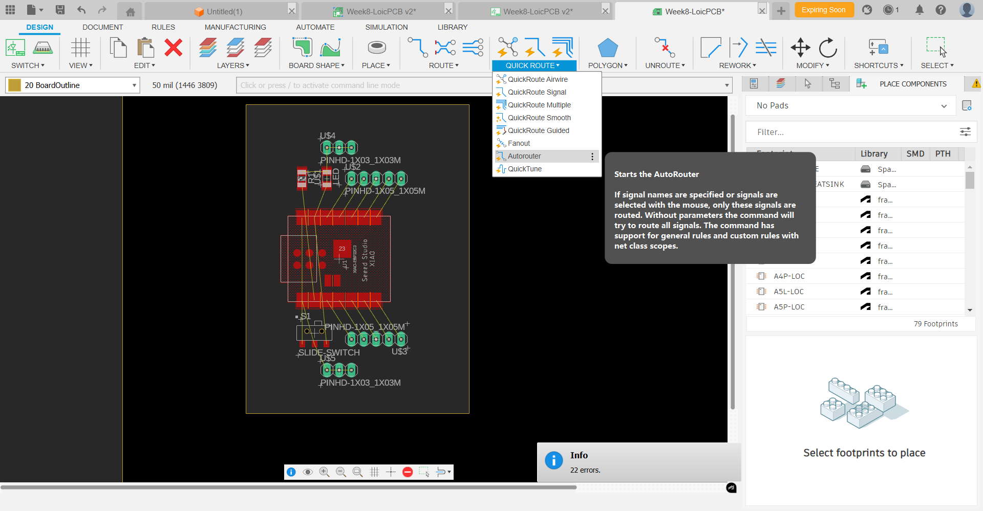
Step 3: Create the routing using the "Auto-route" function, and refine the 90-degree corners with 45-degrees ones. 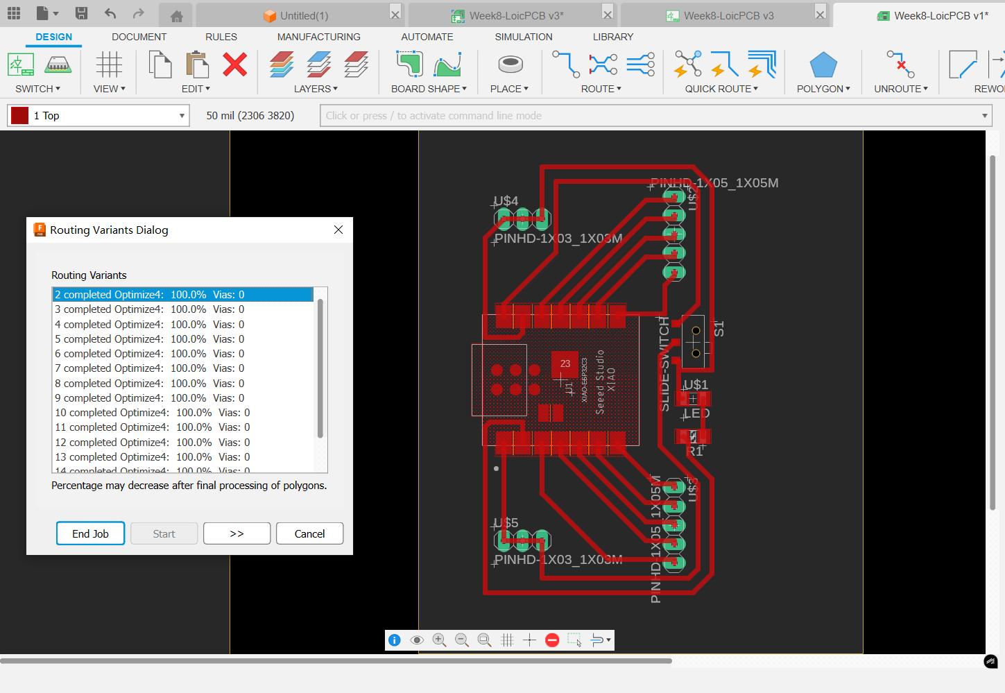
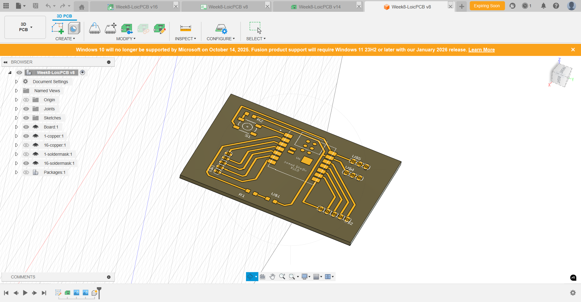
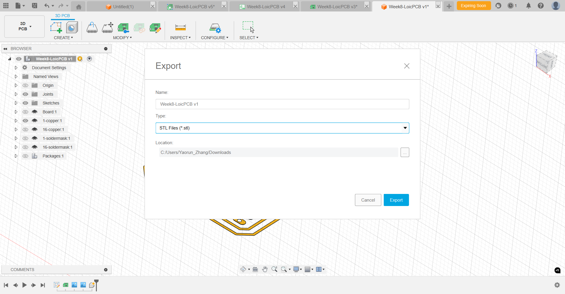
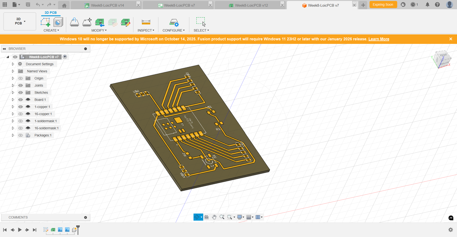
Step 4: Switch to 3D PCB mode, check if any defect, and if all ok... save as STL file the coper layer and the board layer. 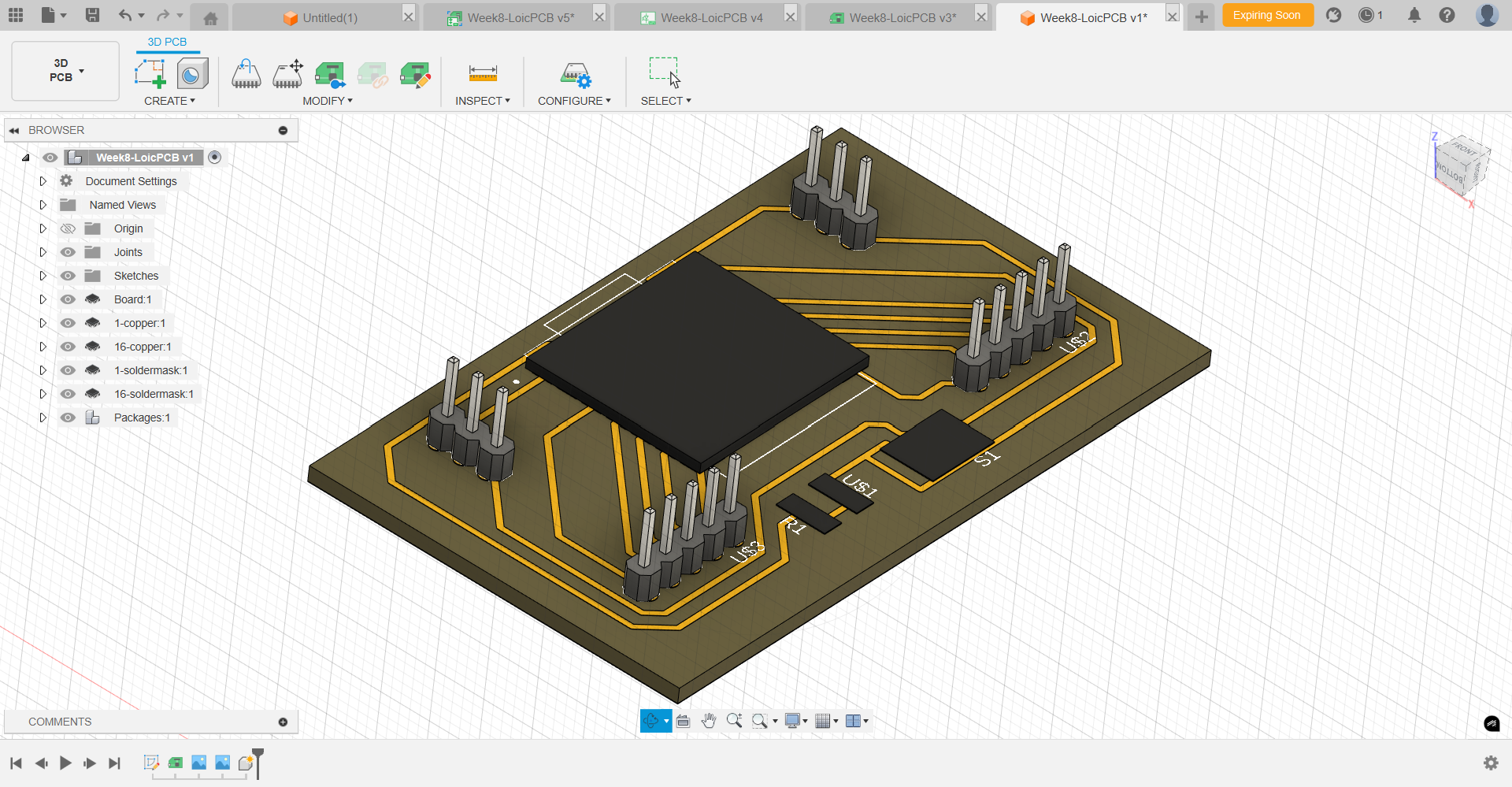
PCB Pre-Production Process
The CAM software used for our Roland MDX-40 is MODELA Player 4, supplied by Roland with the CNC machine.
Step 1: Start the MODELA Player 4 CNC software and "Open" the STL file. 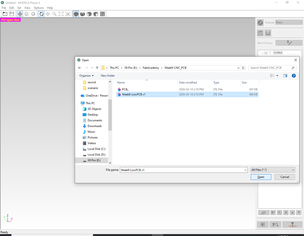
Step 2: Set the material to Brass (1), and set the number of cutting faces to One Face / Top Face (2). 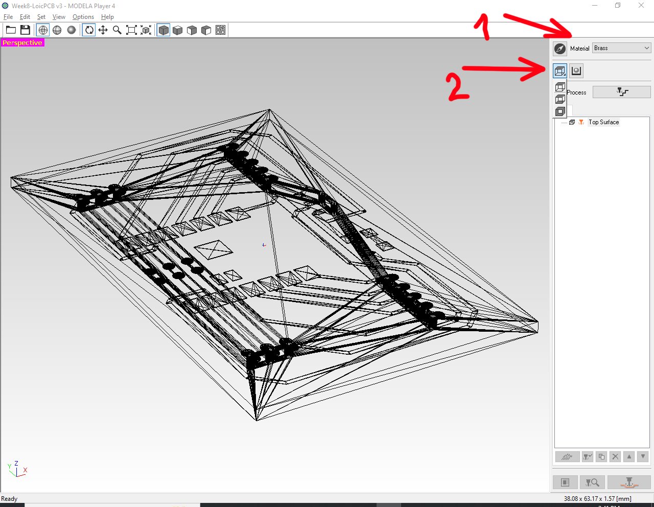
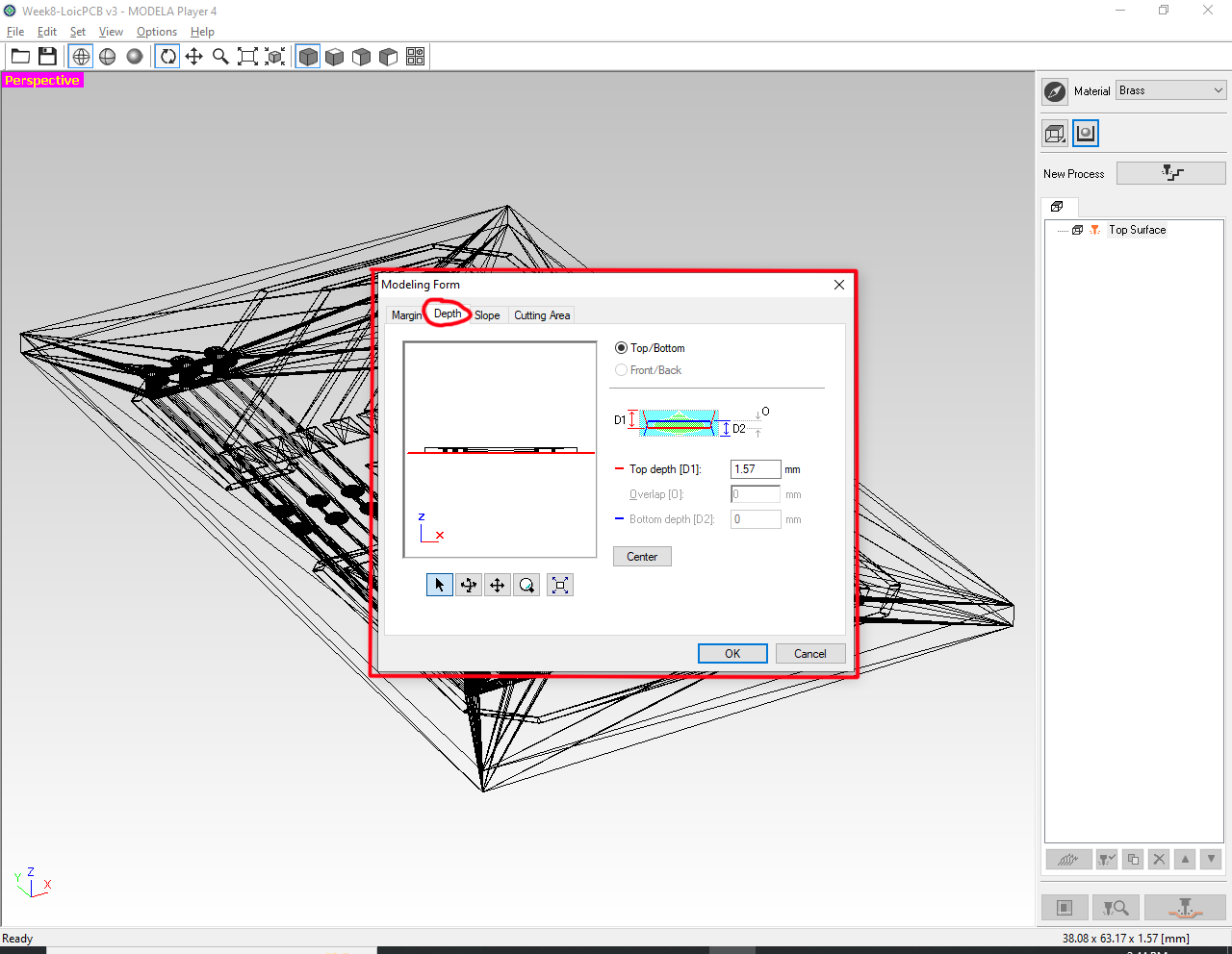
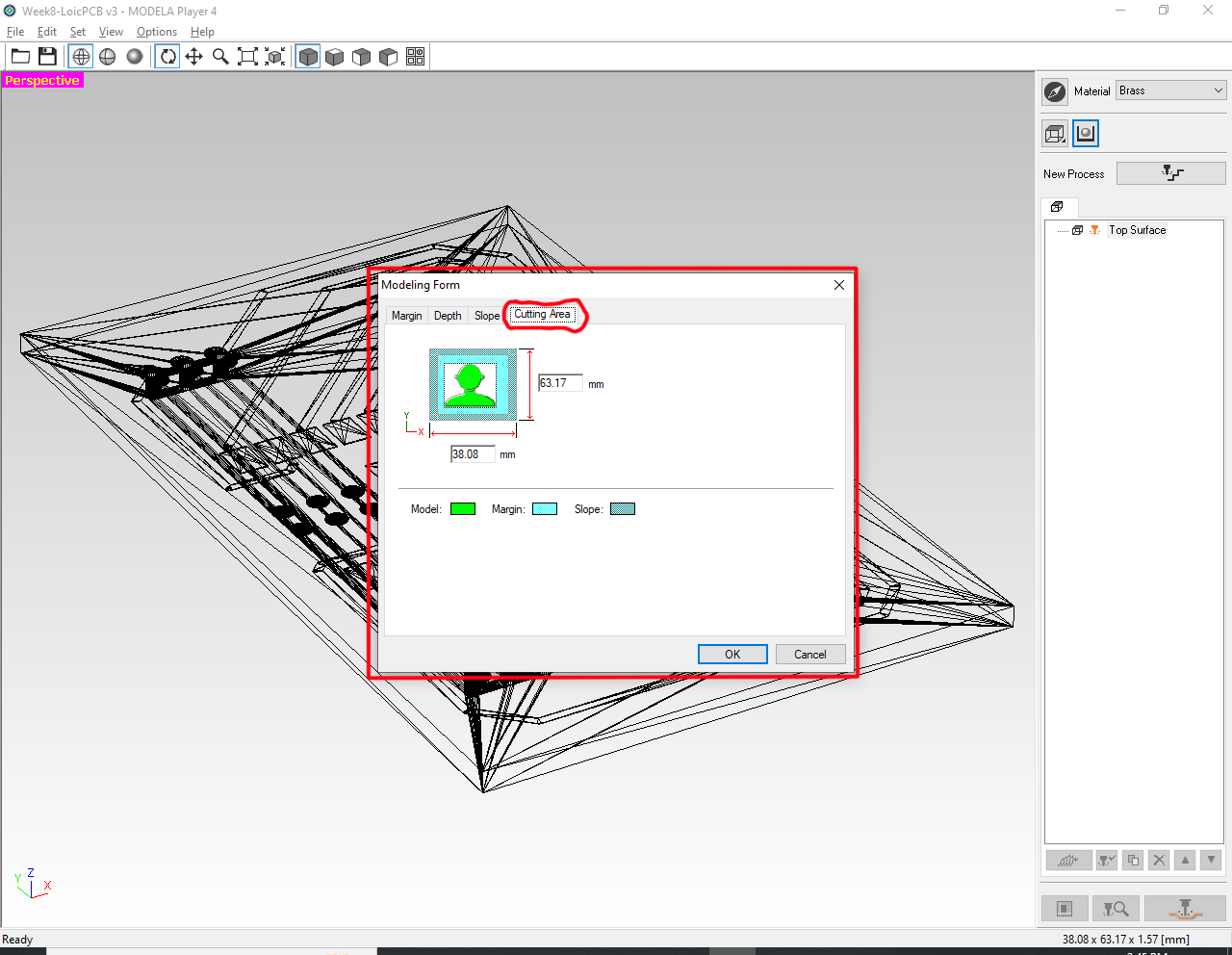
Step 3: Click the Model*ing Form next icon, and check the settings of "Margin", "Depth", and "Cutting Area". 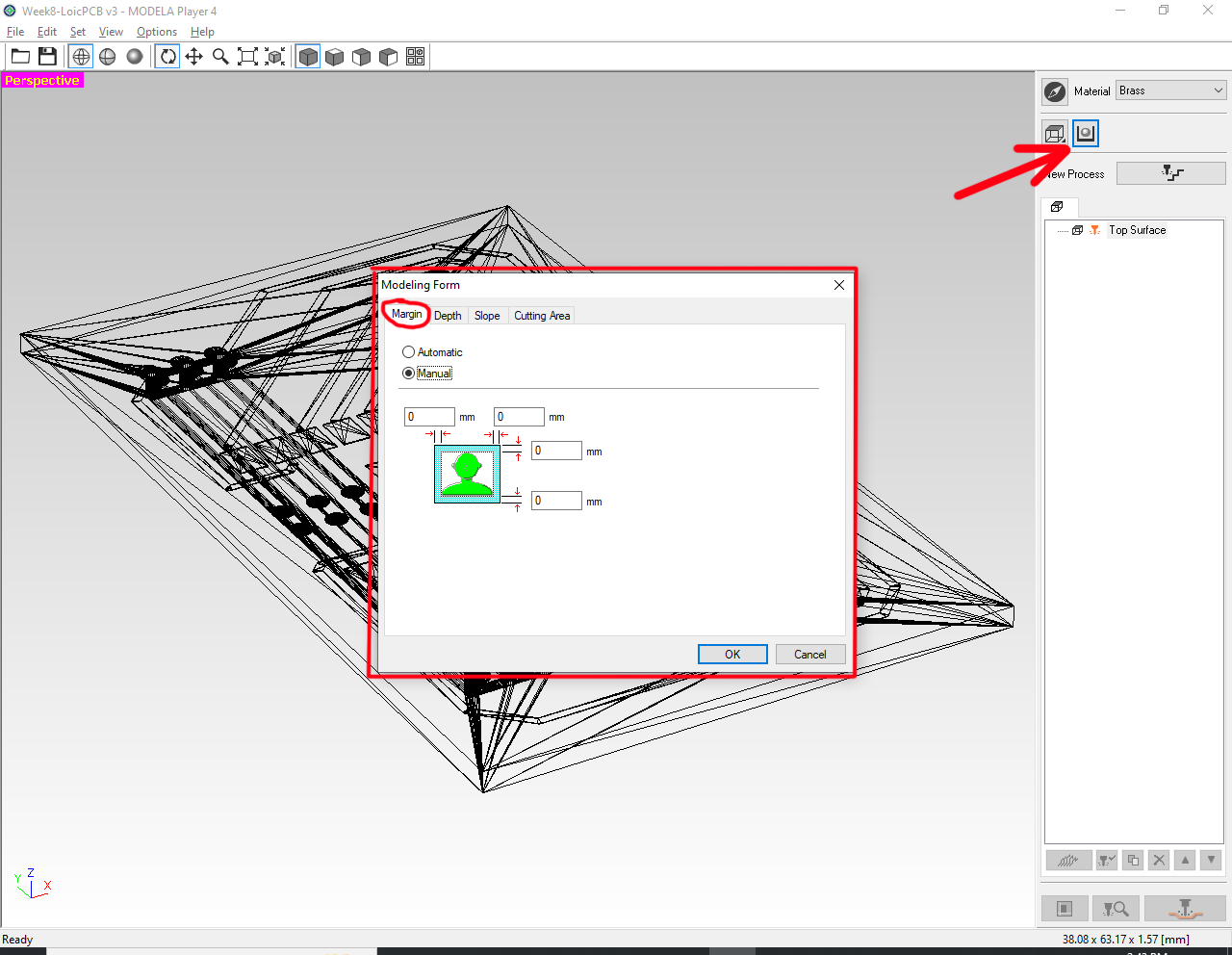
Step 4: Add the machining tool and set the diameter of the tool to be used. 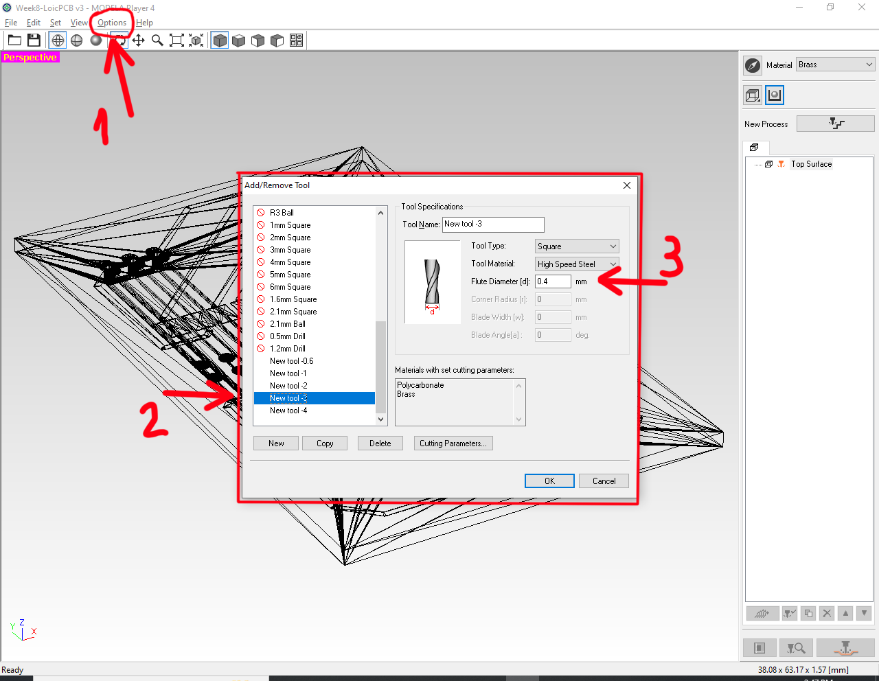
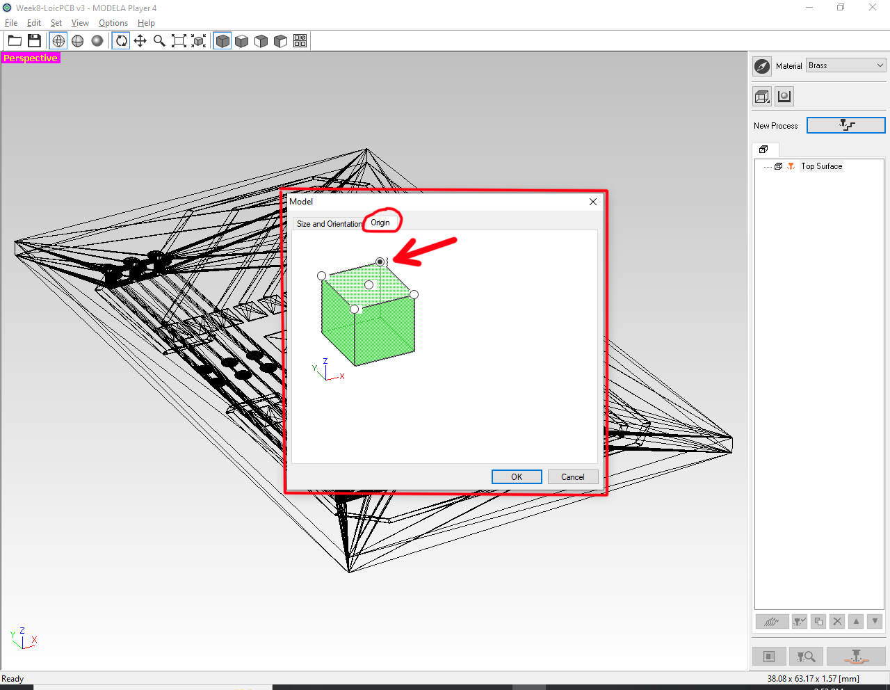
Step 5: Set/check the model "Size and and Orientation", and "Origin". Set the origin to "Upper-Right"... then Click "OK". 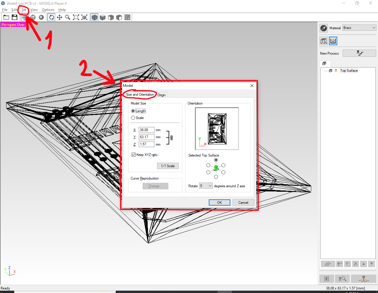
Step 6: Set the machining process by clicking the "New Process" icon (1), and select "Finishing" (2)... then Click "Next". 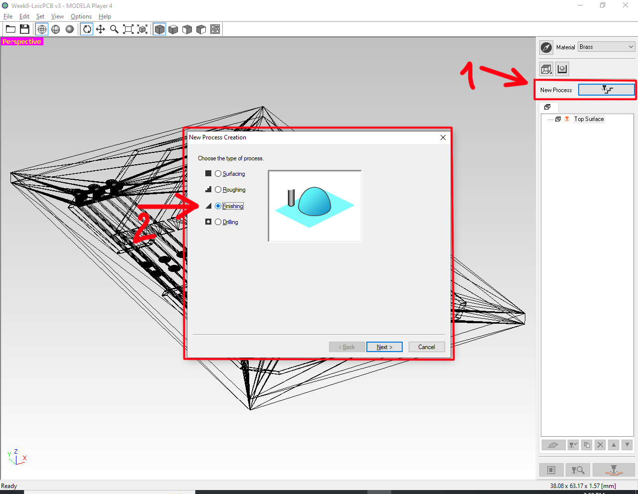
Set the parameters for the "New Process Creation" as follow (1&2)... then Click "Next". 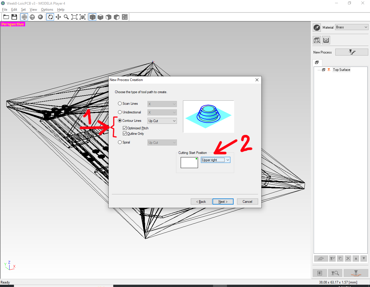
The tool path appears highlighted in blue... 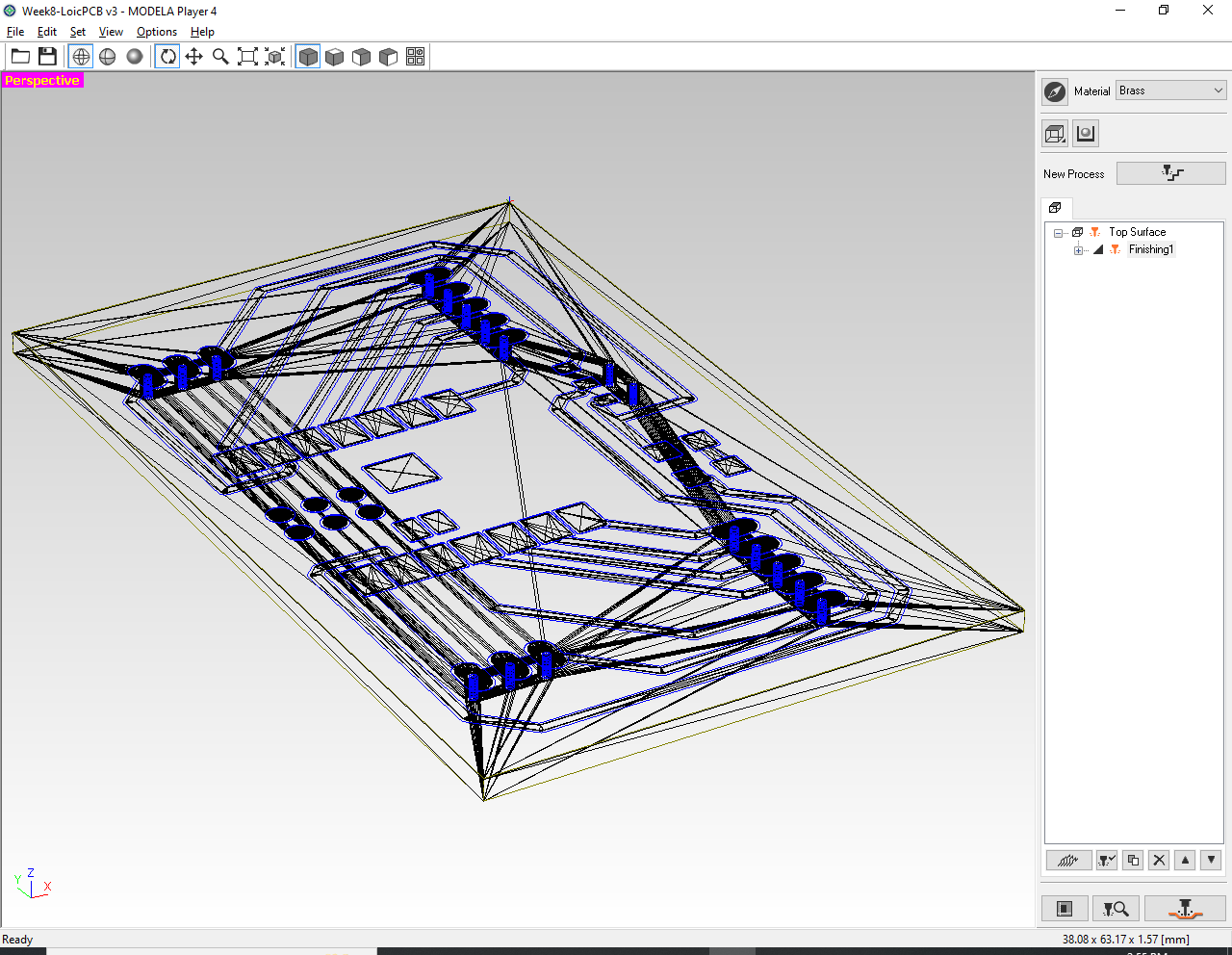
Step 7: Click the "Preview" icon (1) to display the "Virtual MODELA" result of the machined PCB (2). 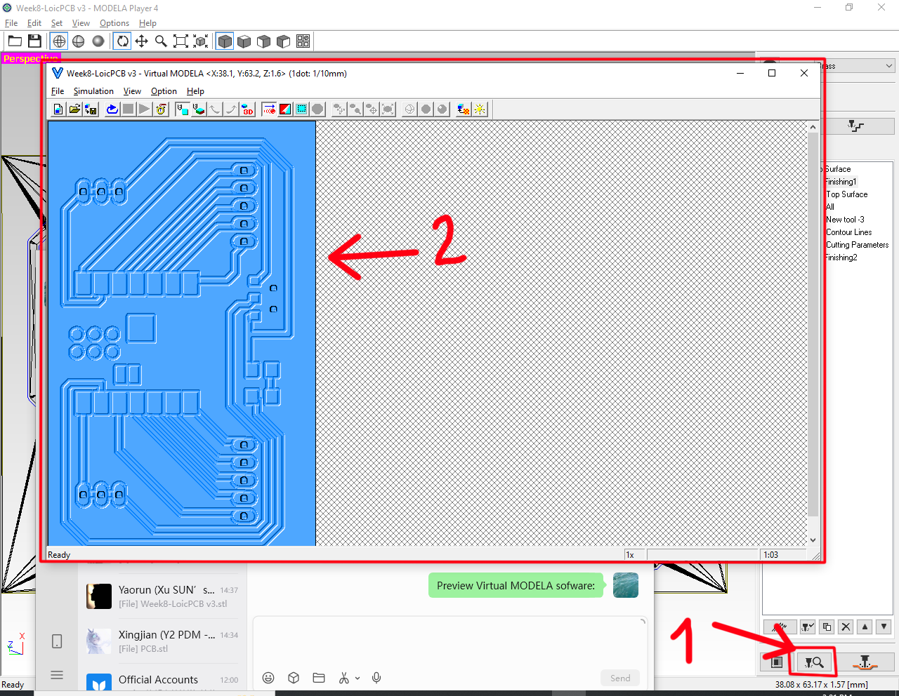
PCB Production
OHHHH!!! 3 failures** 😦 😦 😦
Failure 1: The connection wire-pad is broken 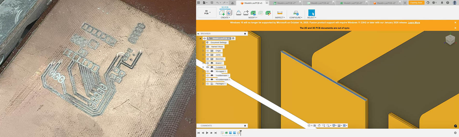
Failure 2 & 3: The bed is definitely not leveled and the wire width too thin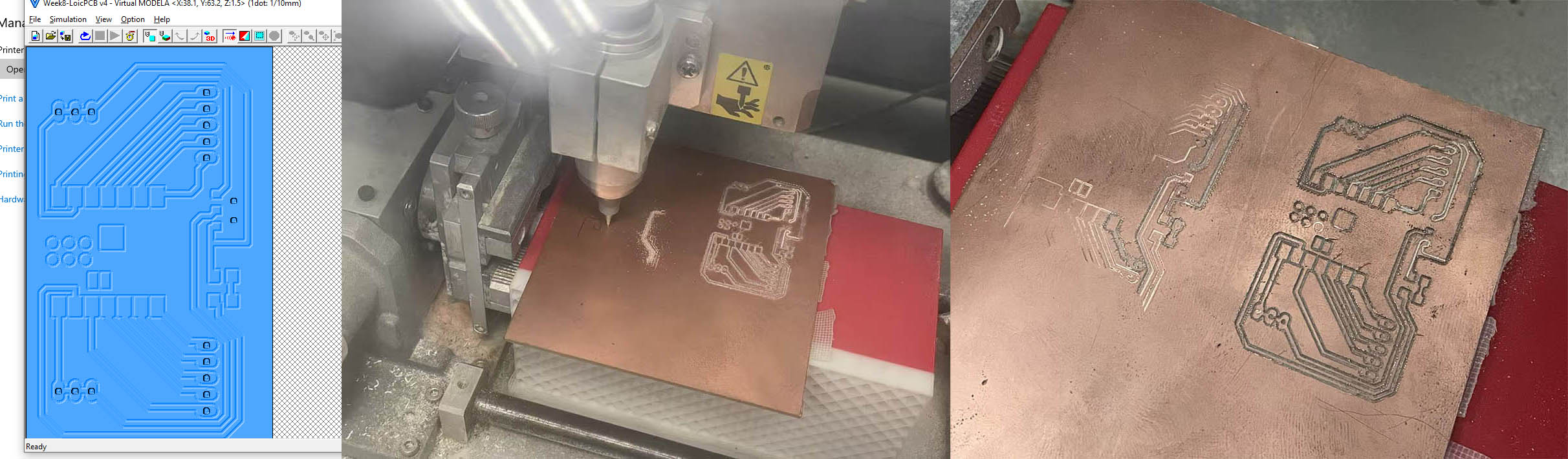
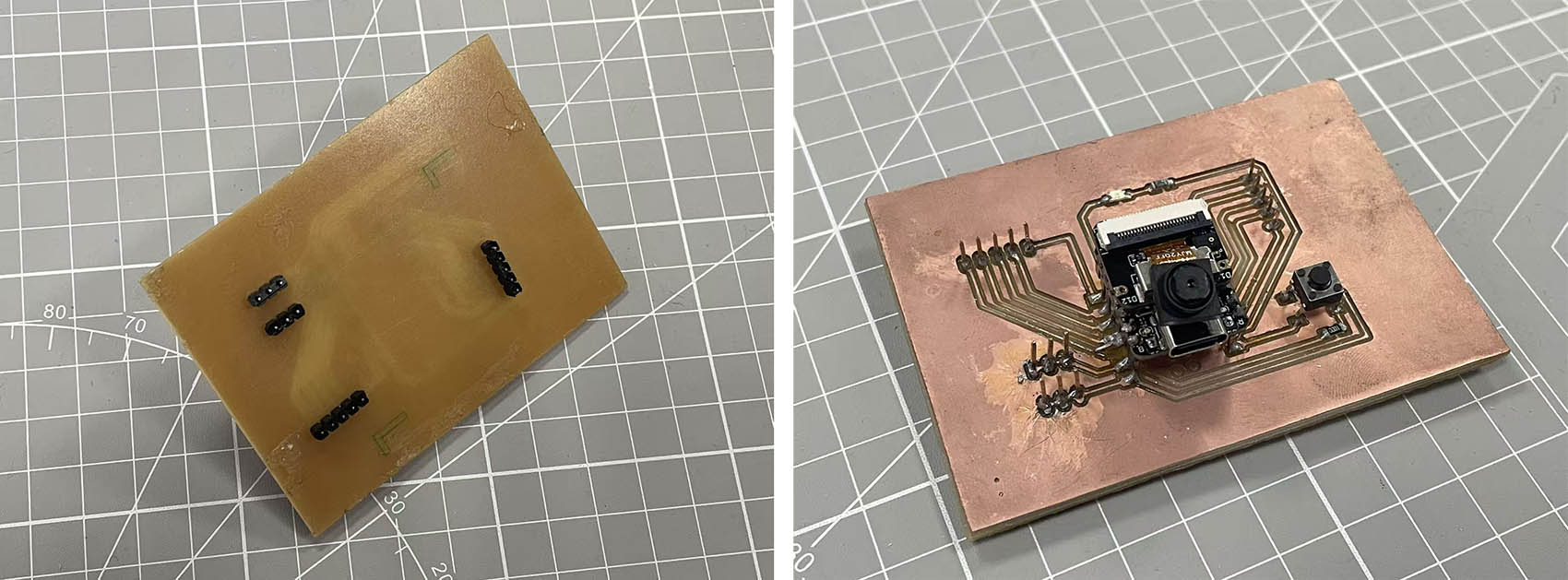
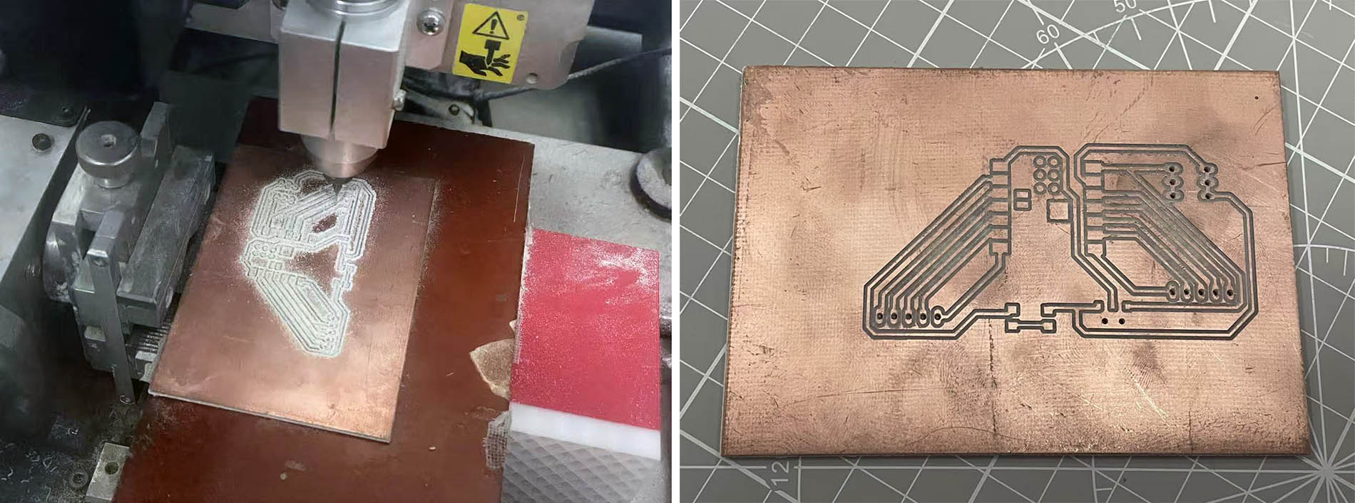
Fourth trial is SUCCESSFUL!!! 😃 😃 😃
The wire width has been increased from 24mil to 32mil. The PCB material has been changed from FR1 to FR4. The new board is more rigid, helping on eliminating the defects on the surface.
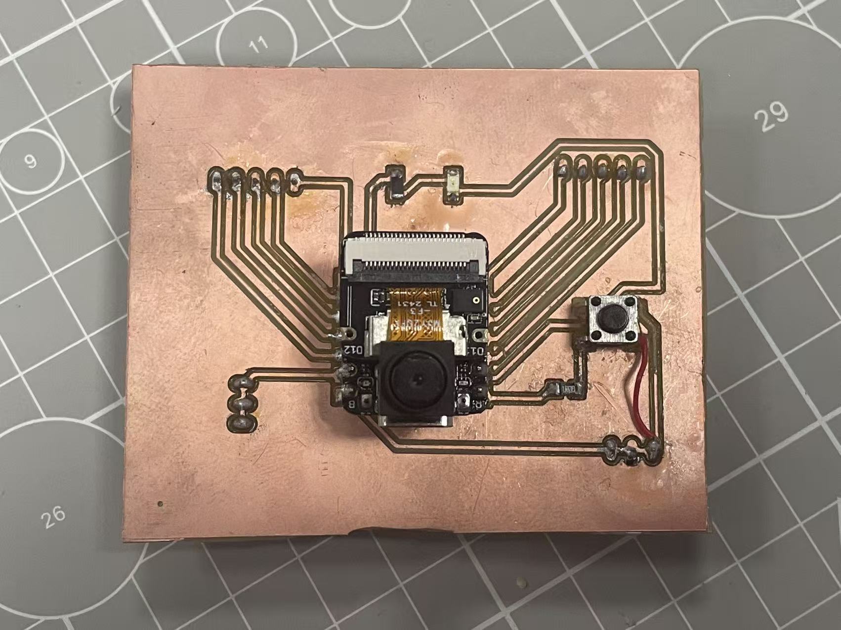
Soldering and Assembly of the PCB extension Board
First, a bit of training on soldering (that was a few days ago)... 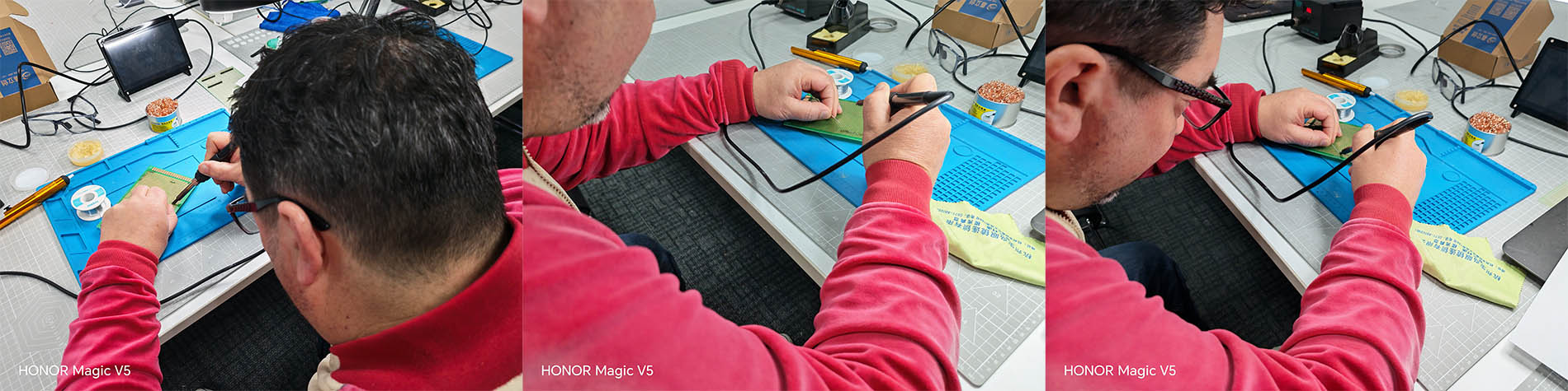
Today, a 5-Pinhead component has been succesfully welded on the board... at my first attempt 😉 😉 😉 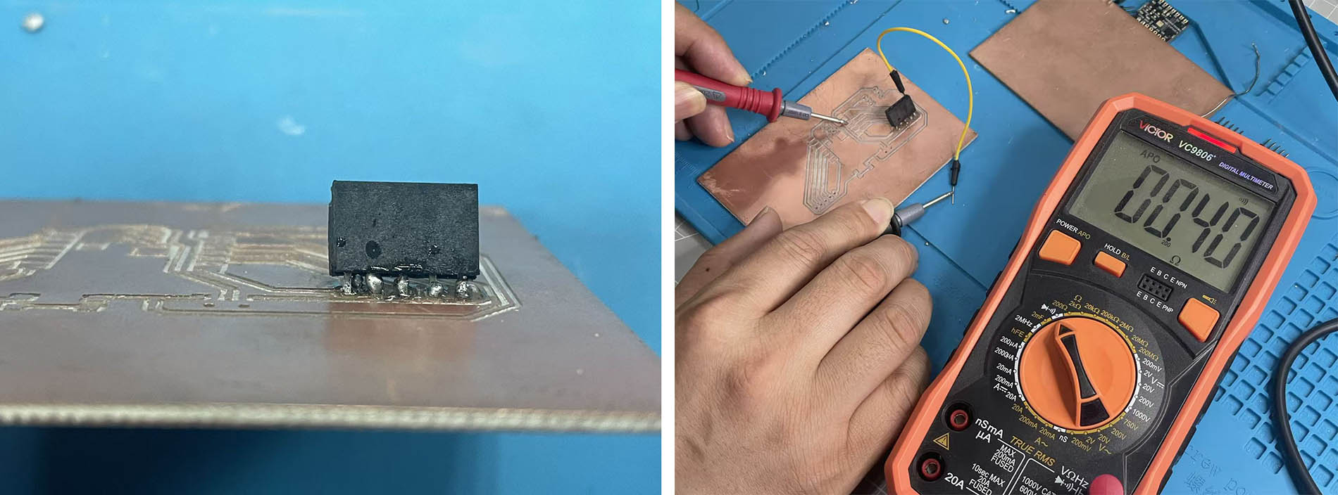
Then, after successfully soldering the 3 other pinhead components, I realised that the design of my PCB board uses the "WRONG" switch format according to what we have available at my Fab Lab... 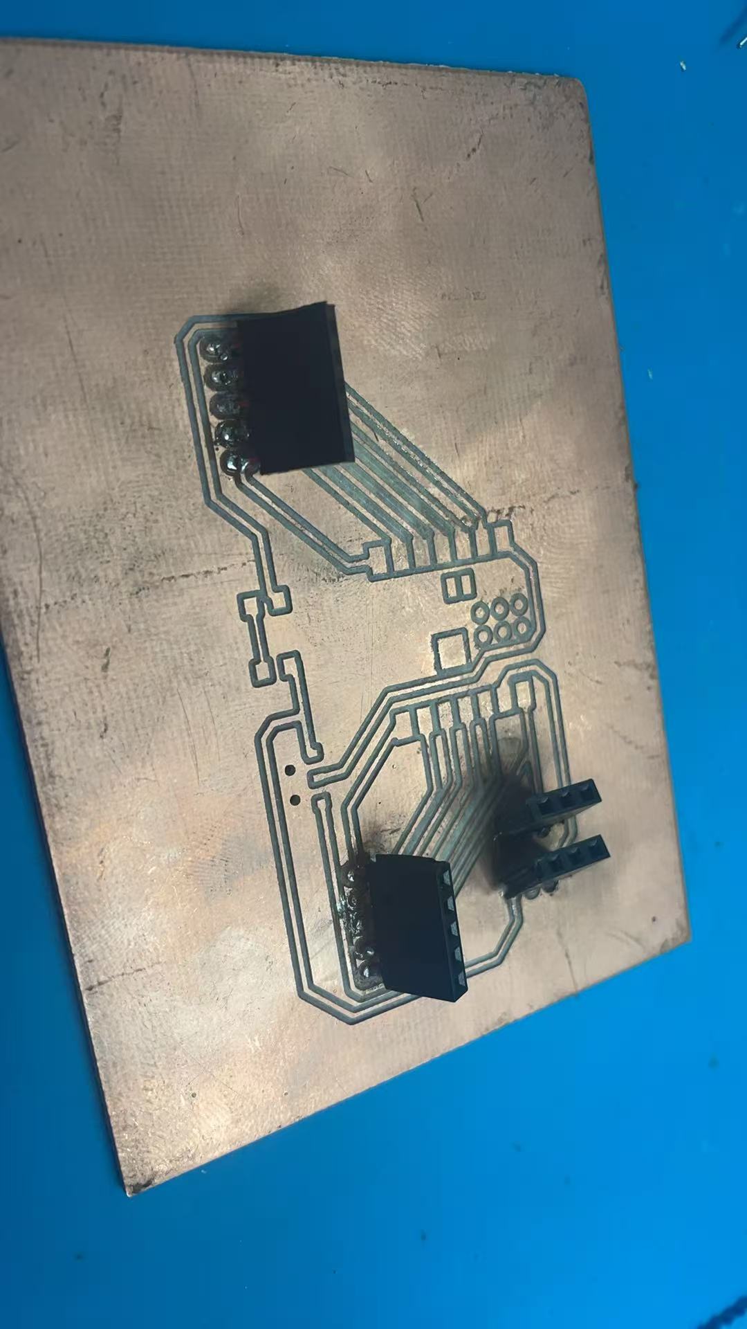
...So I have to review the shematic design of my PCB board and produce a new one!!! 😦 😦 😦
ROUND FIVE for the Production of my PCB (...but not final yet) 😦 😦 😦
I take this opportunity to include a Switch 6*6, and also correct the orientation of the LED (in my original schematic the LED was in the wrong direction). 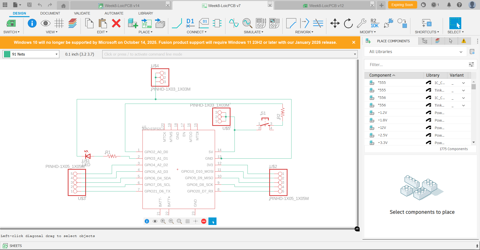
Machining of the "ROUND FIVE" PCB board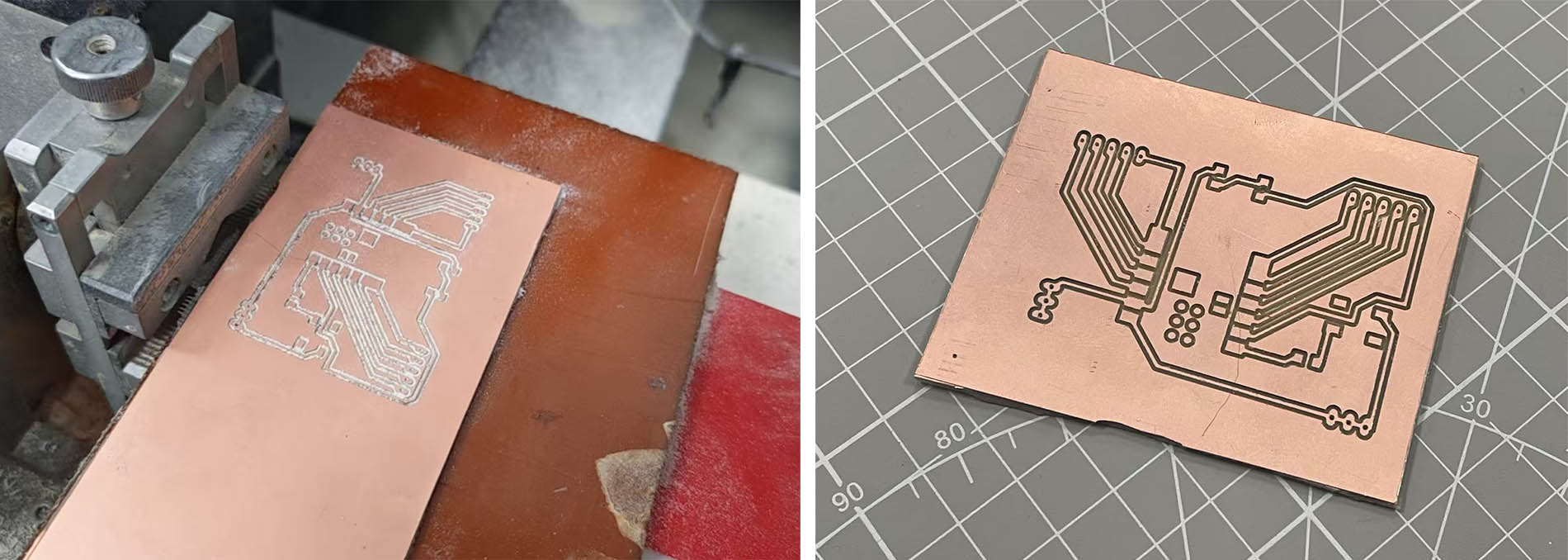
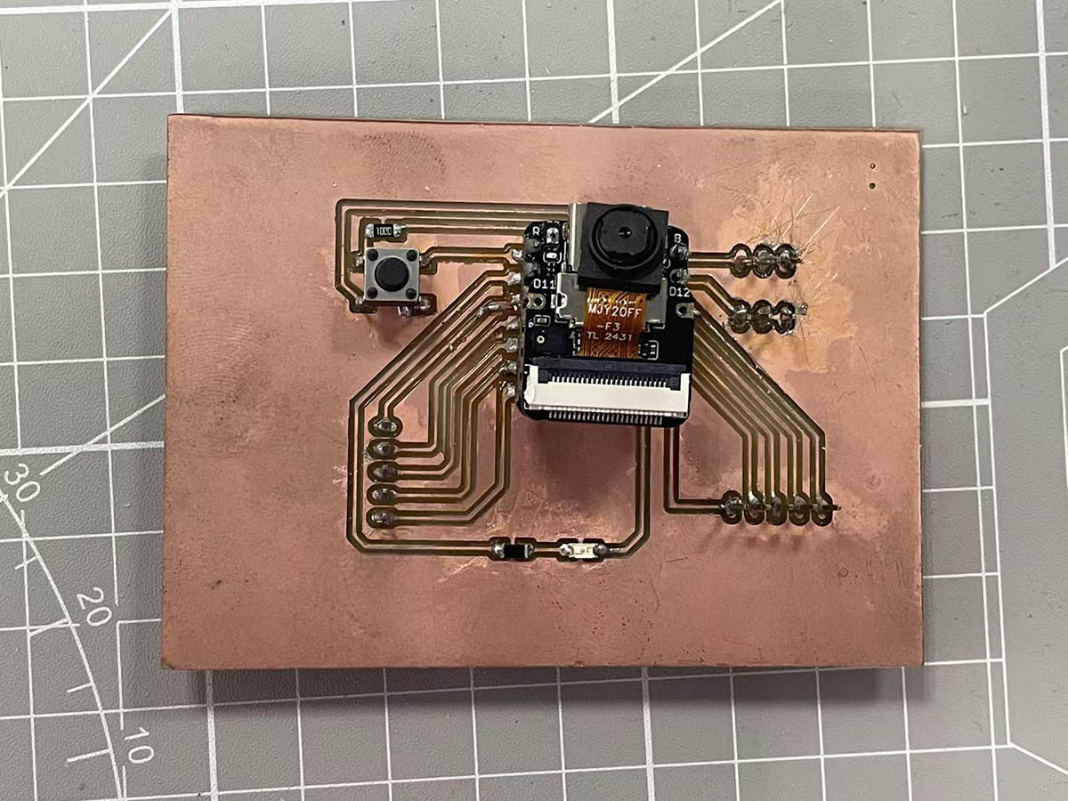
The switch 6*6 initially soldered on the board was defective (only realised it when testing after assembly). I damaged the copper layer when removing it. I tried to use glue to fix the problem but the glue didn't dry. So, I decided to weld a wire (in red) to solve the problem. 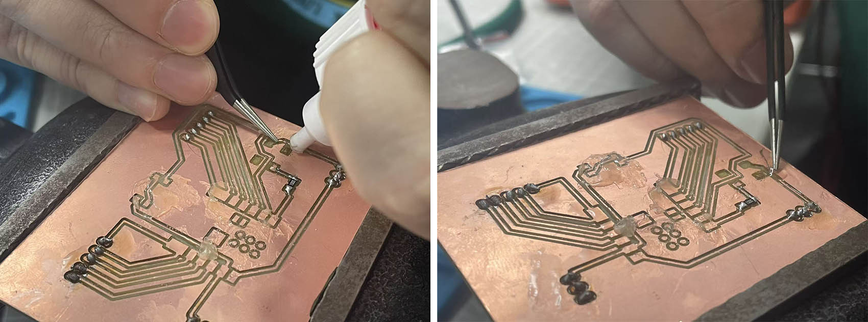
"ROUND FIVE" complete PCB board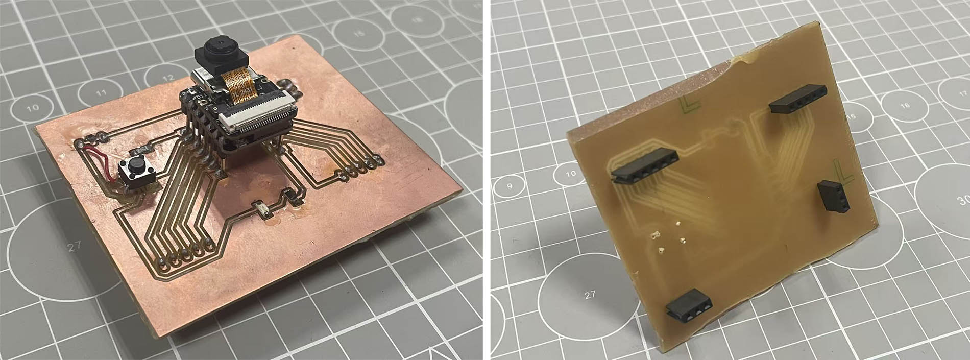
...but I made a mistake with a wrong wiring of the Switch and connecting the Resistor to D0 pin instead of the GND pin 😦 😦 😦 ...a "ROUND SIX" is necessary 😭 😭 😭
ROUND SIX for the Production of my PCB (...and final!!!) 😃 😃 😃
All is correct this time...