Appearance
WEEK 6 – Electronics Design
Assignments
Group Assignment
- Use the test equipment in your lab to observe the operation of an embedded microcontroller
Individual Assignment
- Simulate a circuit
- Use an EDA tool to design an embedded microcontroller system using parts from the inventory, and check its design rules for fabrication
- Extra credit: try another design workflow
- Extra credit: design a case
Group Work
Our group work is accessible HERE (add the link)
Individual Work #1
PCB Design Process
Project Initialisation
Step 1: After reviewing a few EDA platforms with my instrutor, such as KiCad, Altium, Cadence, and EasyEDA/IcDEA... I decided to use IcEDA for this week first trial. EasyEDA/IcDEA is a free open-source EDA software. The IcEDA is the Chinese version which can be set in English, and the EasyEDA version is the international version.
Step 2: This is the home interface of the software - Click "New Project" to create a new project 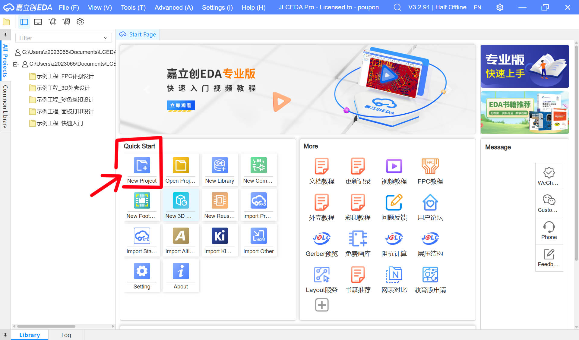
Step 3: Define file name and its location on my laptop, and then click "Save"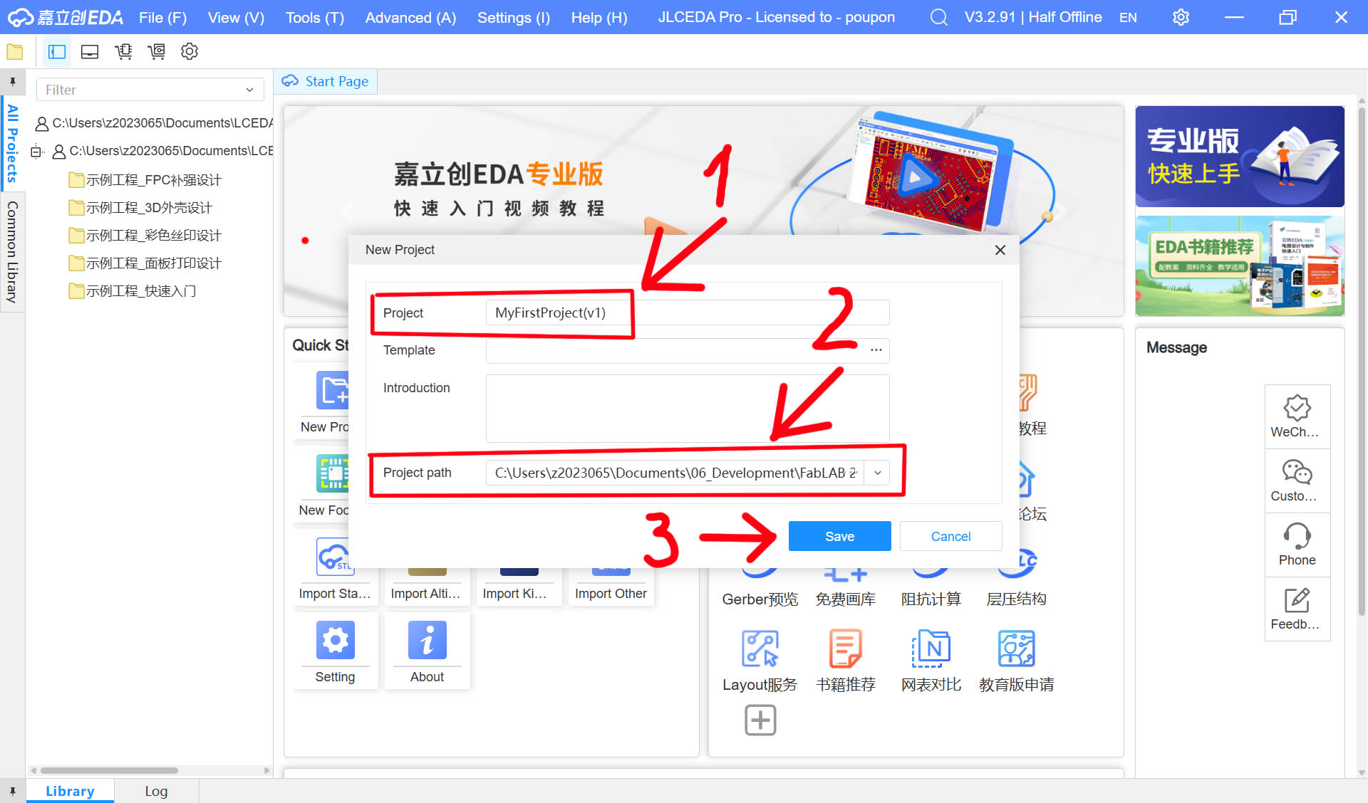
Step 4: The new project file is created and the software interface updated 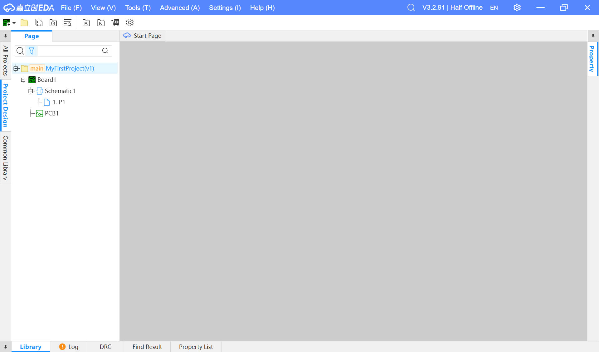
Step 5: Double-Click P1 to make visible the skecth page and frame template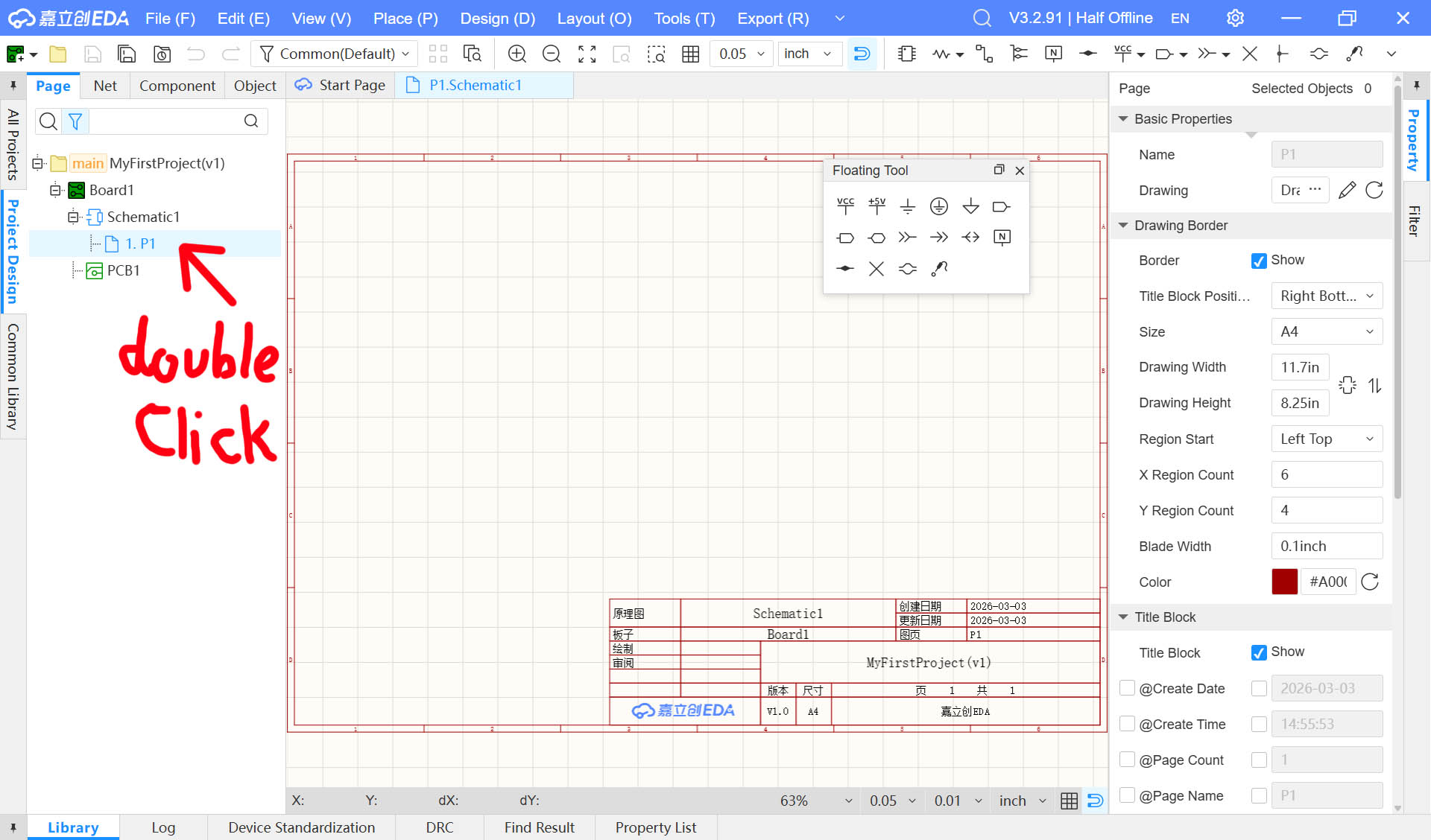
Import Components from the Component Library
Here is the process to import my first component, the XIAO-ESP32-C3, which I decided to use for this practice exercise.
Step 1: Click the "Library icon"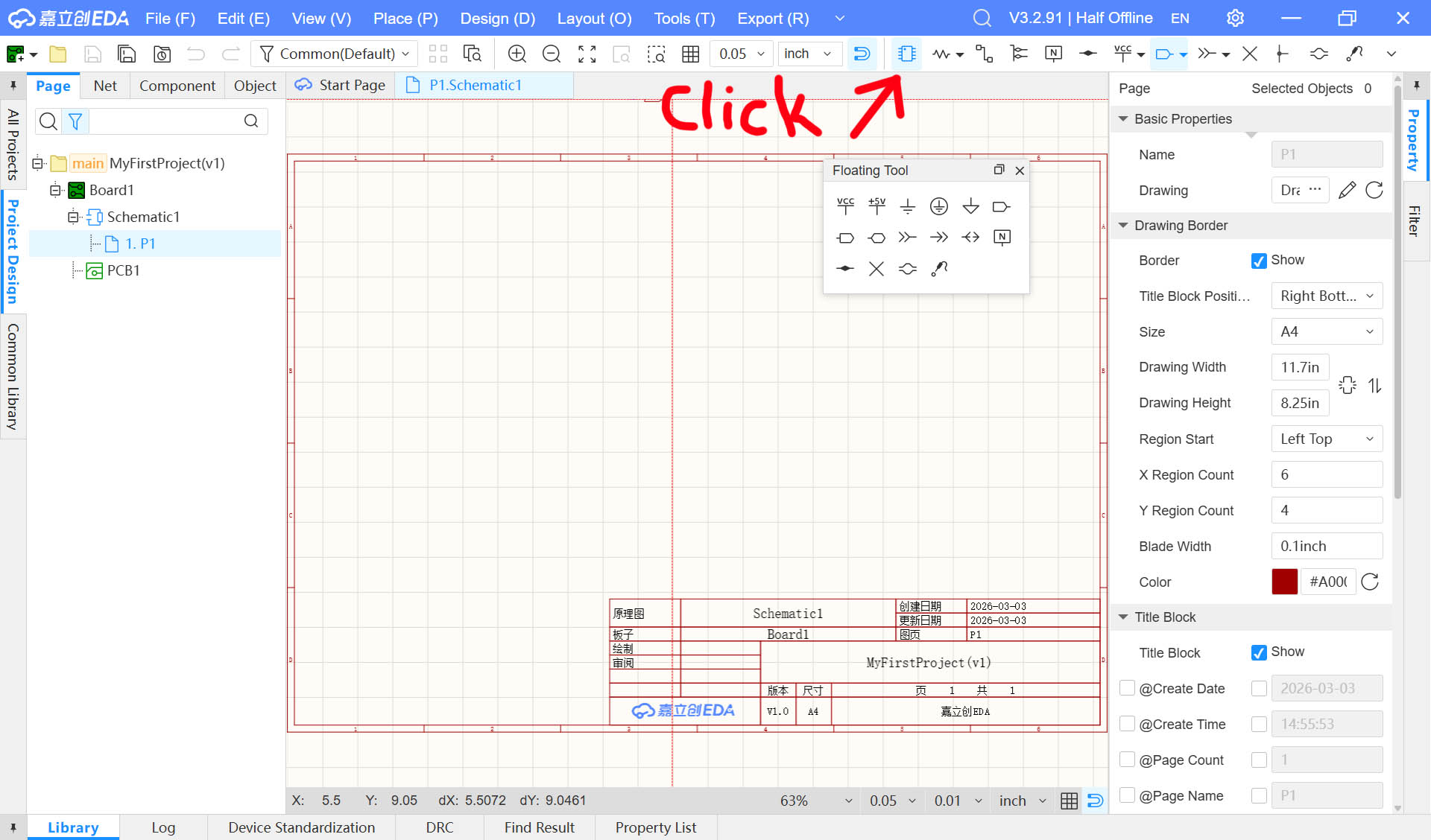
Step 2: Select the "JLCEDA library", then type the name of the board we are looking for, the XIAO-ESP32-C3, then click the "Place" button for the relevant one (see below "Hardware Specification Analysis" section)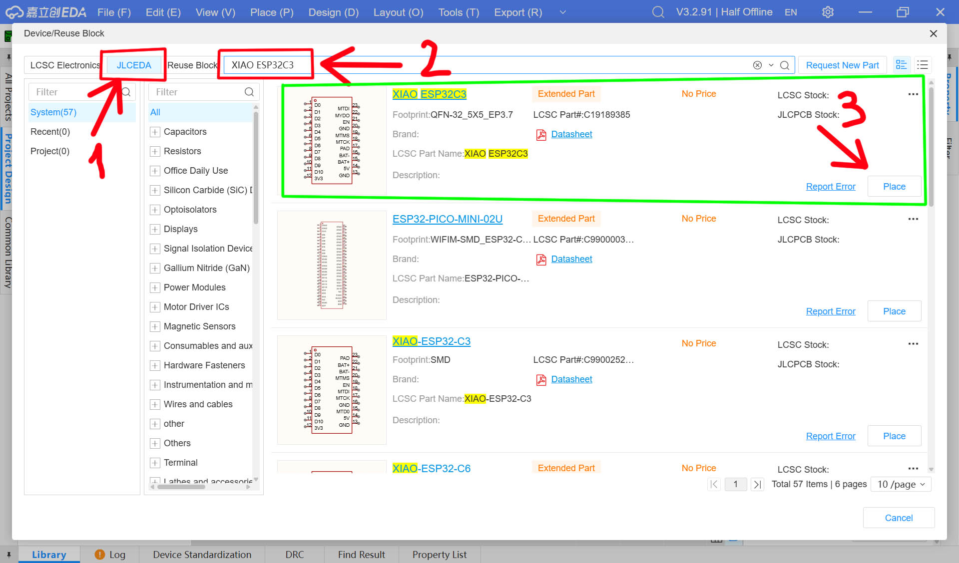
Step 3: Click anywhere in the displayed page space to place it on the schematic page P1 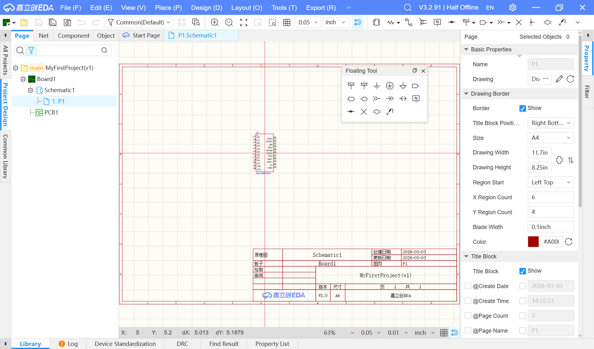
Step 4: Repeat Step 1 to 3 to import from the JLCEDA library in IcEDA the other required components for my electronic design scenario as listed below:
- x1 LED (NCD1206G1)
- x1 Resistor (150Ω) - as recommended on the datasheet of the LED
- x1 3-pin Head for SG90 Servo
- x1 4-pin Head for Ultrasonic Sensor HC-SR04
Hardware Specification Analysis
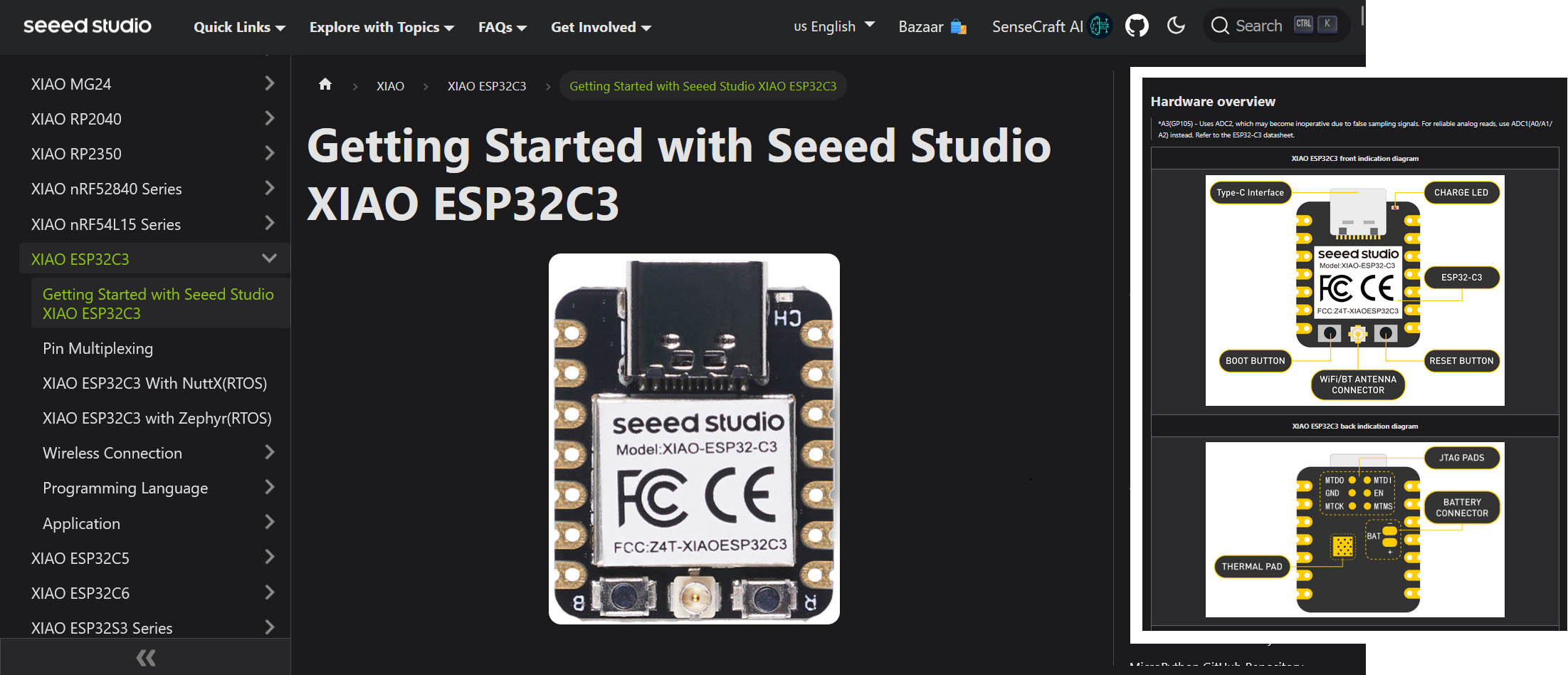
Before going any further in my Electronics Design, I must better understand the specifications and Pin definitions of the hardware, the XIAO-ESP32-C3. To do so, I looked for a "Getting Started" tutorial on the XIAO-ESP32-C3.
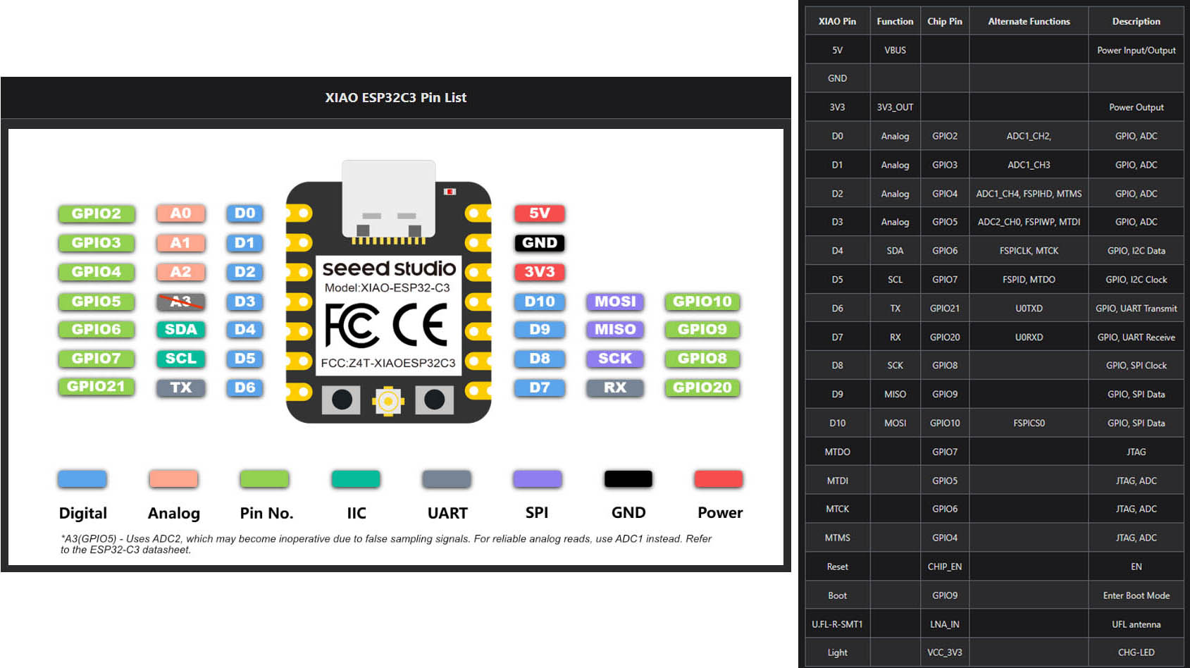
Pin Assignment Plan
Here below is my plan for connecting the pins:
| Pins (IAO-ESP32-C3) | Signal Name |
|---|---|
| A0 | Ultrasonic Sensor TRIG |
| A1 | Ultrasonic Sensor ECHO |
| D7 | Servo PWM |
| D9 | LED + |
| GND | LED - / Ultrasonic Sensor / Servo PWM |
| VCC | Ultrasonic Sensor / Servo PWM |
Circuit Design Implementation
Schematic Design
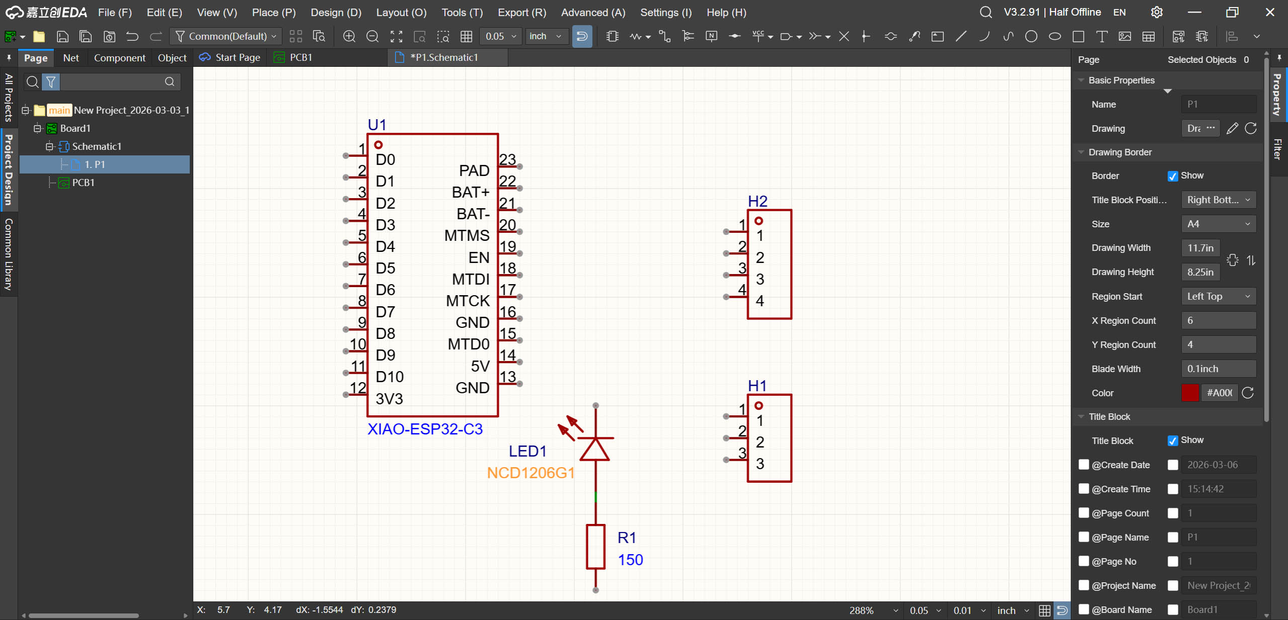
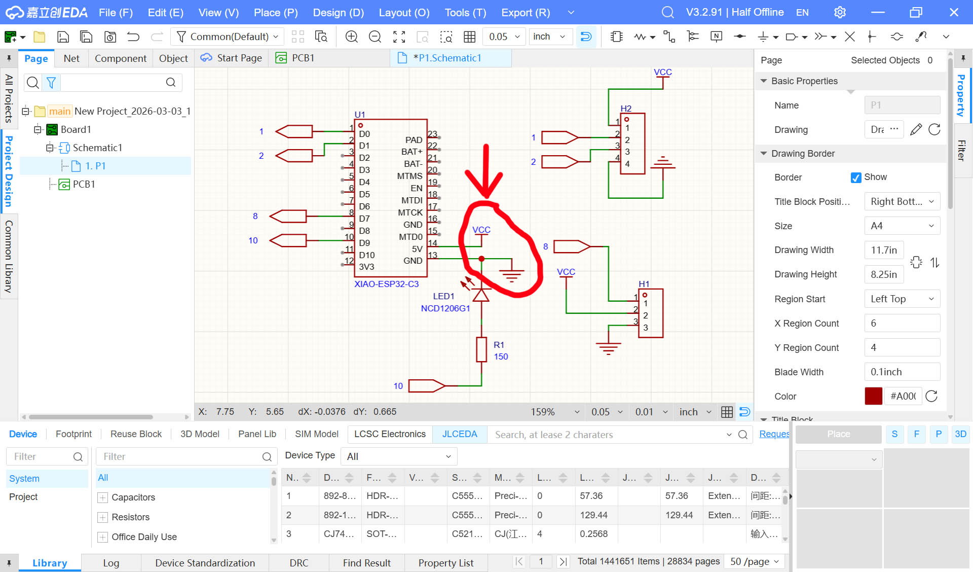
Step 1: Connect the components to the appropriate pins of the IAO-ESP32-C3 micro-controller as shown below, using wires and connectors: 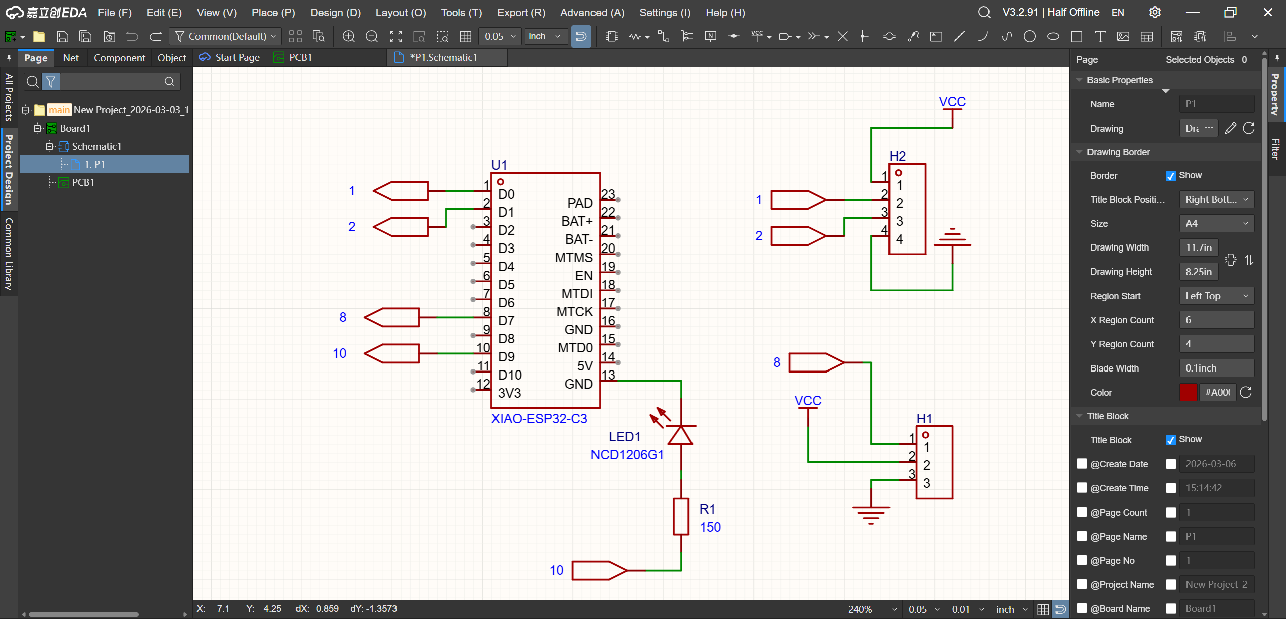
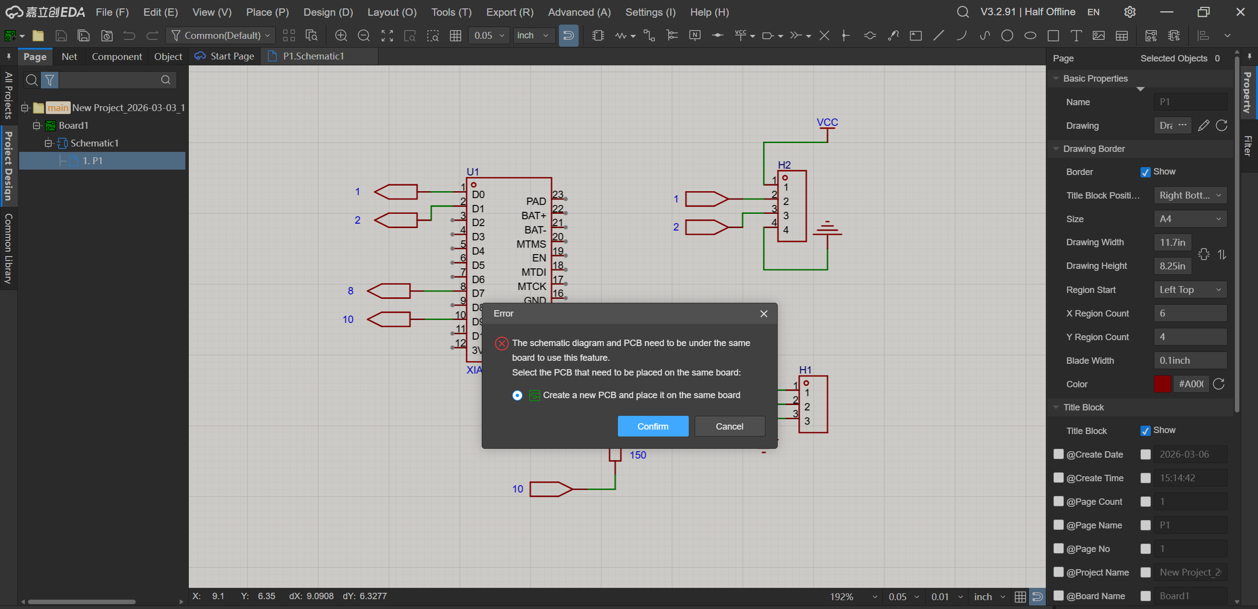
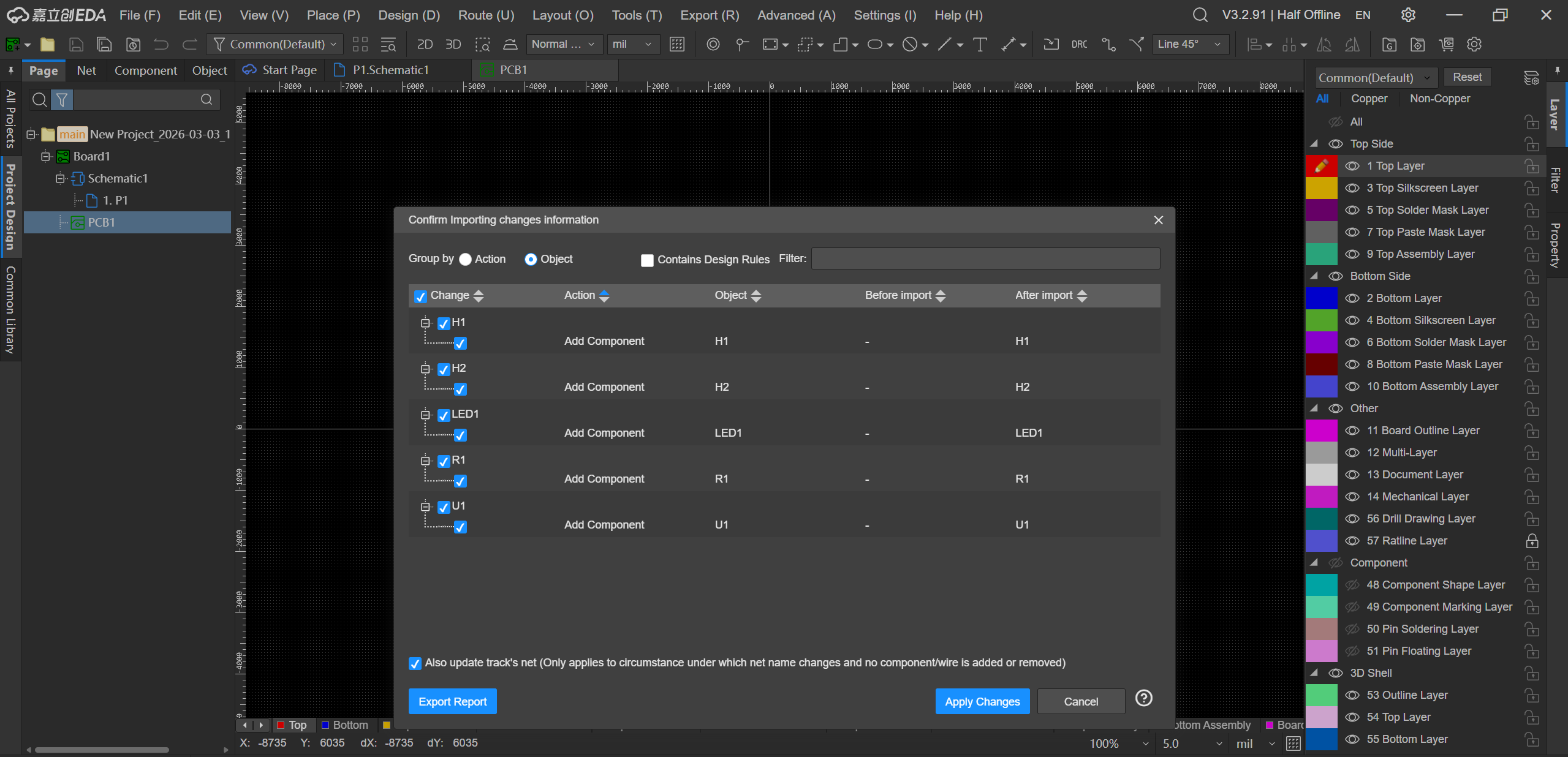
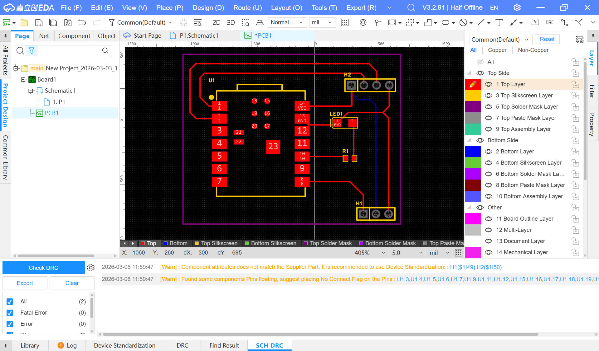
Step 2: Convert schematic to PCB. It is needed to "Confirm" to create a new PCB and place it on the same board. It is also required to "Apply Changes" to confirm importing changes information. 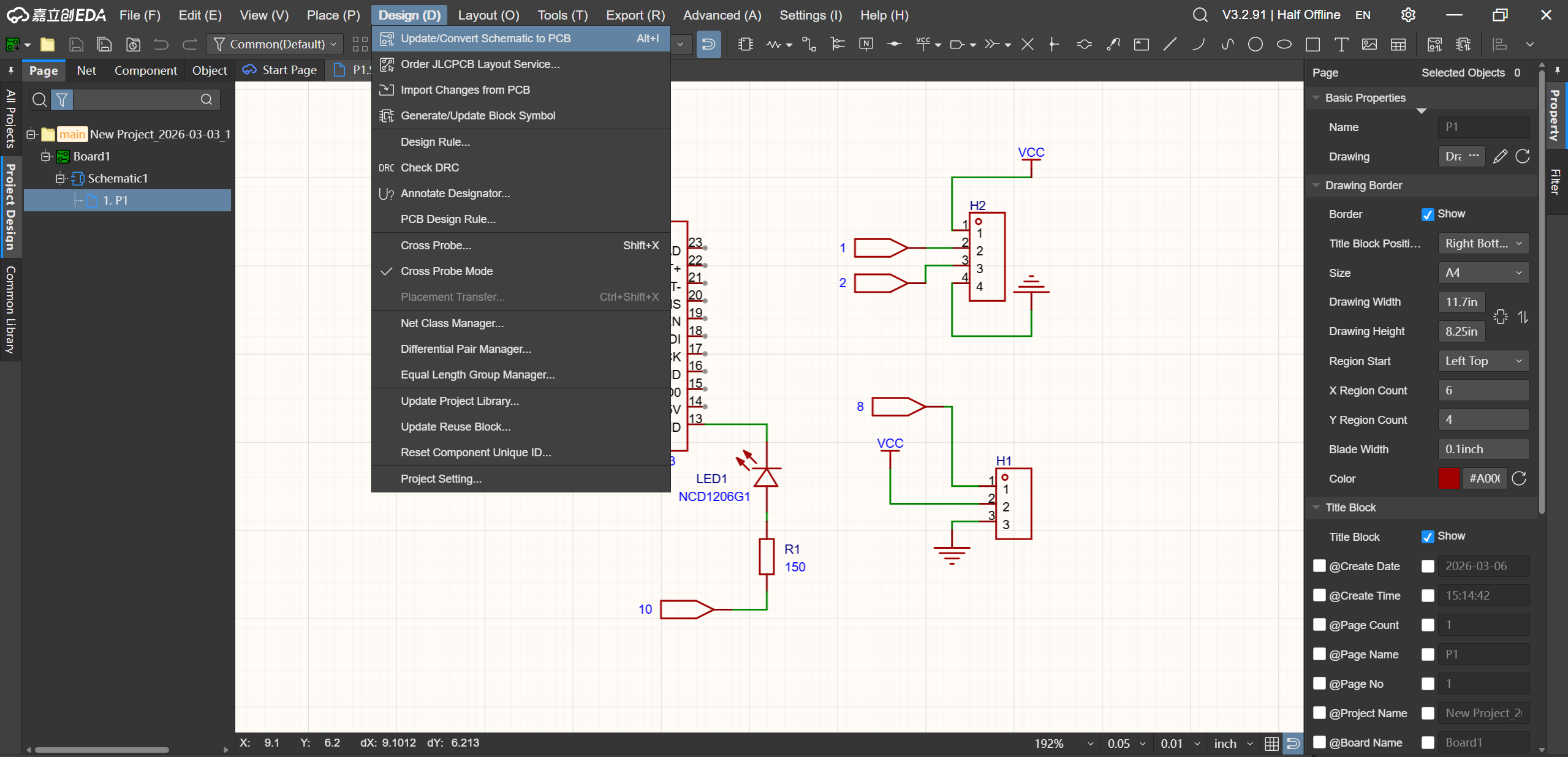
Here is the result: 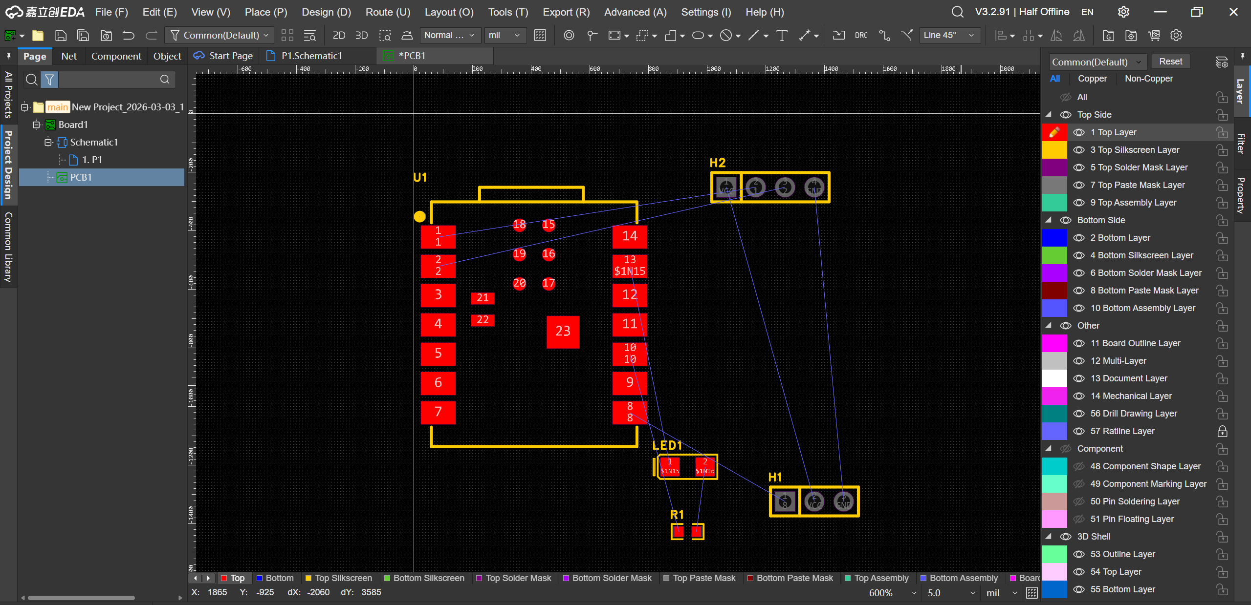
PCB Layout and Design
Step 1: Now, we need to re-arrange the layout of the components on the PCB to optimise its size, clarity and routing complexity. 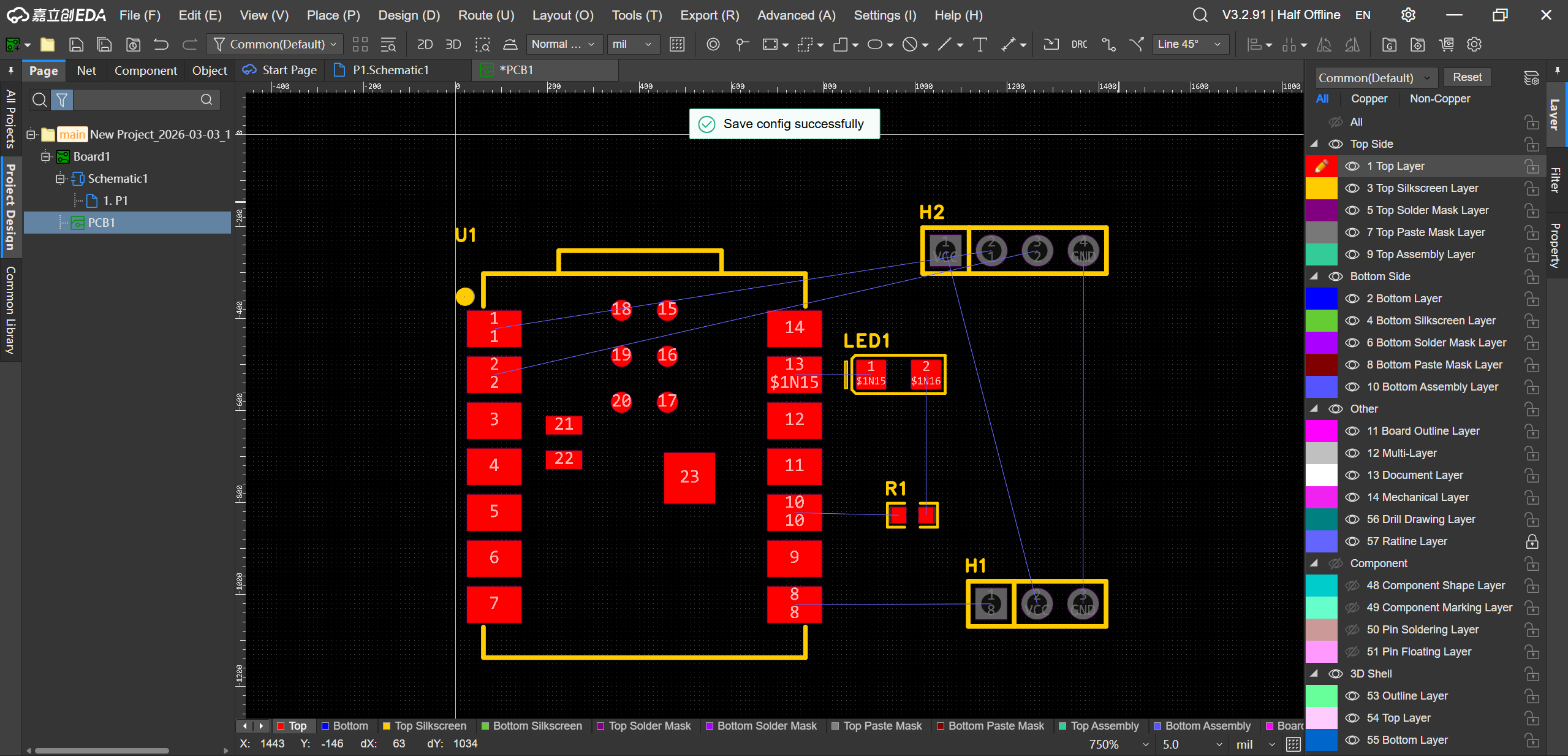
Step 2: Define the outline of the PCB. 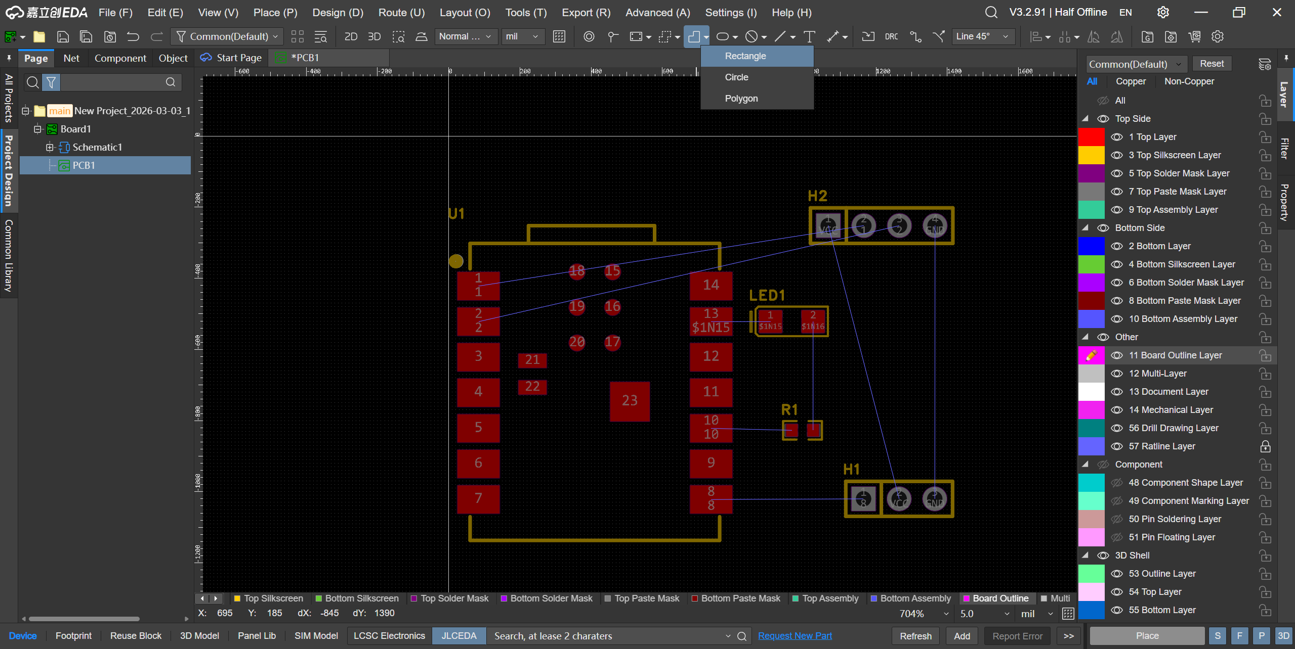
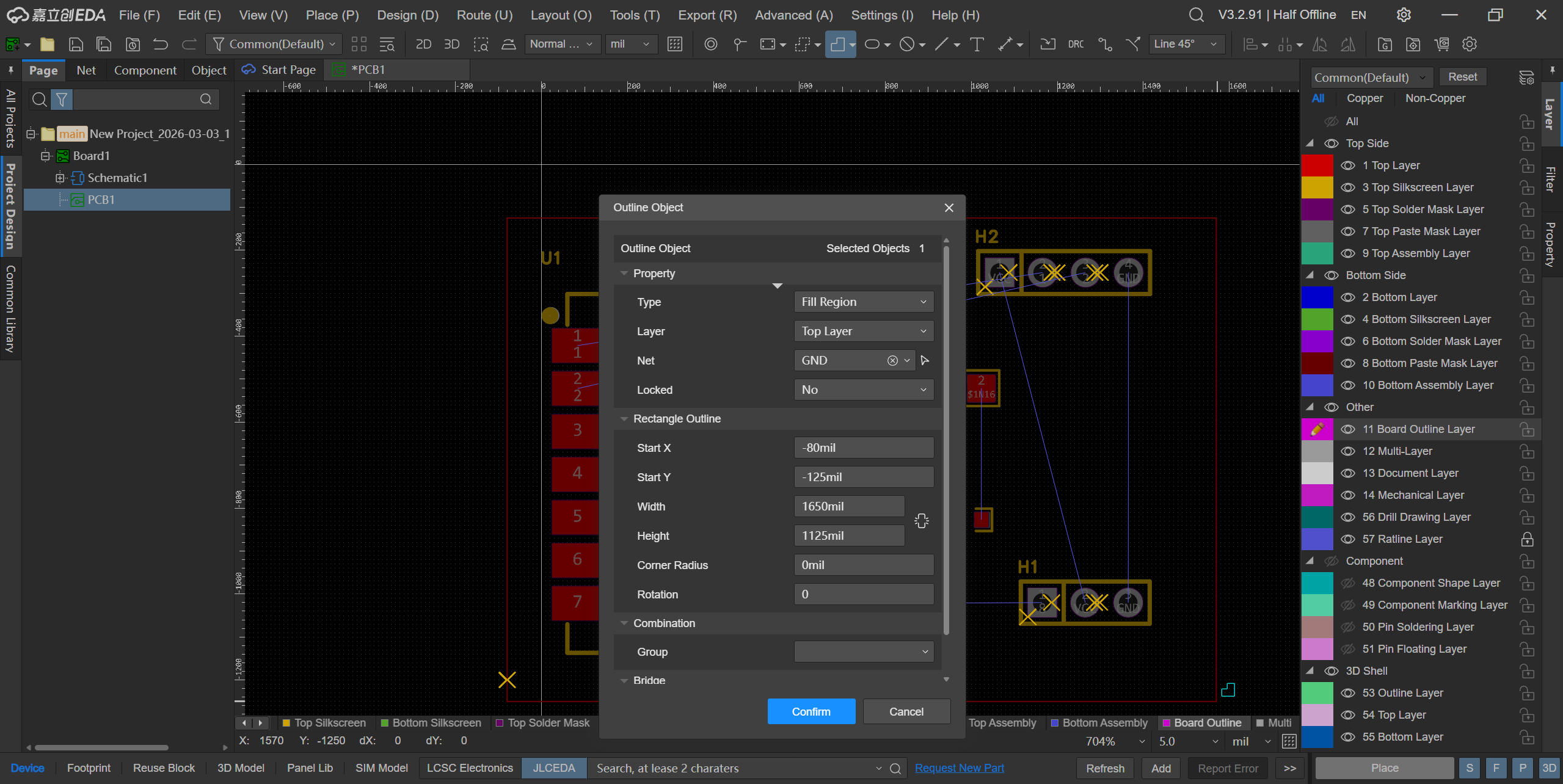
Here is the result: 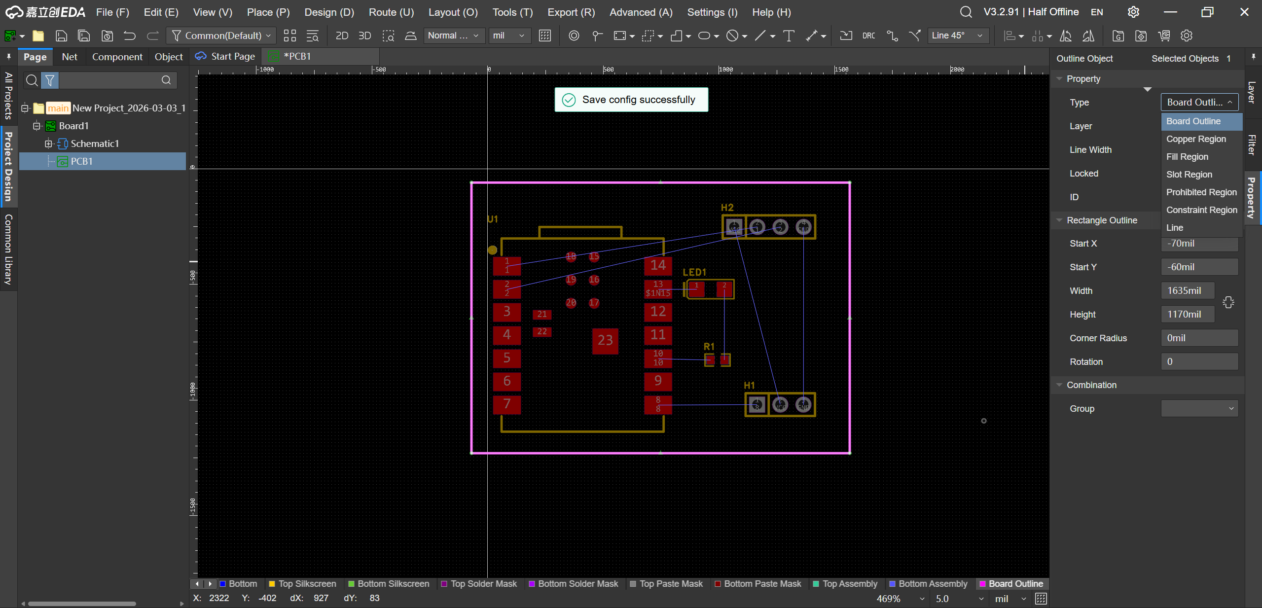
Step 3: Create the routing by clicking "Auto Routing" in the "Route" top menu, and check/set the parameters (Design Rules) before clicking "Run". 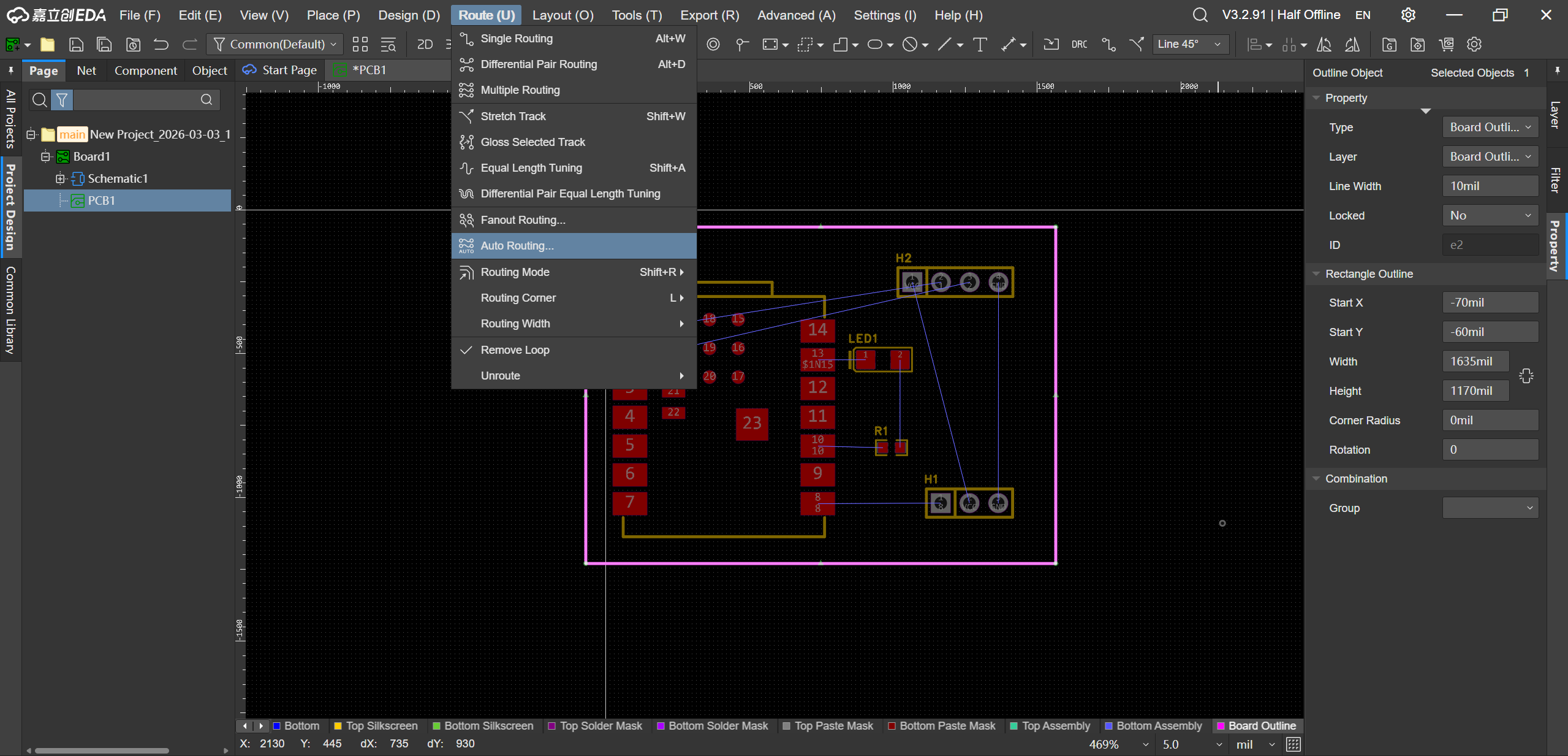
Here is the result: 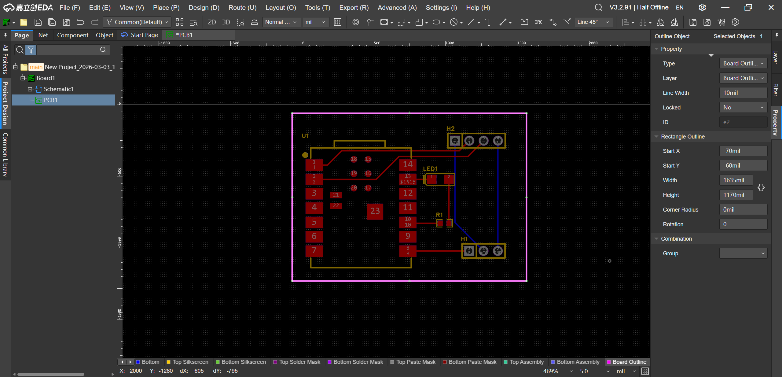 Looking at the result in the image above, we can identify two problems:
- The wire connecting Pad 2 is crossing the connection pads for the battery, and therefore should relocated
- The blue wires are on the bottom face of the board and should be moved to the top face for manufacturing simplicity
Step 4: Wiring improvement according to the two above listed recommendations. 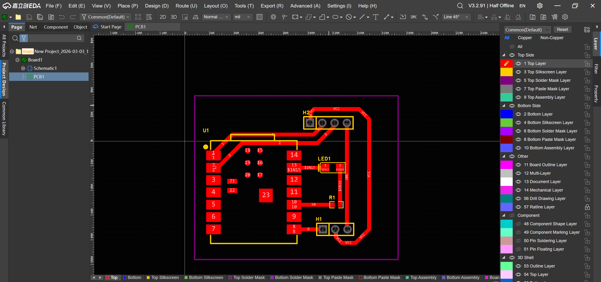
OHHHH!!!! MISTAKE...
I forgot to connect the VCC and the GND to the Pinhead 😦 😦 😦
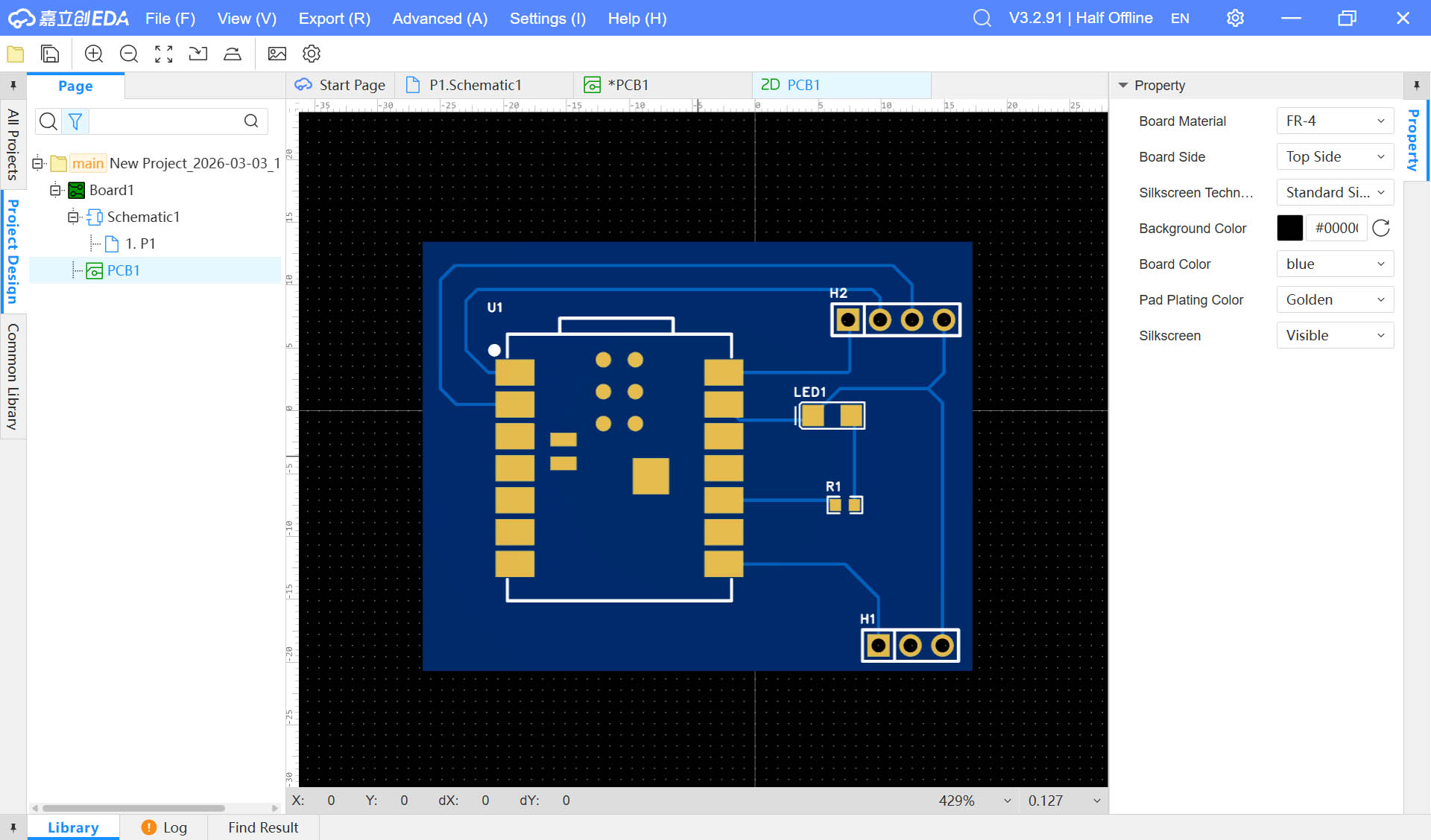
Final PCB Design
Wire View
2D View
3D View
Individual Work #2
For this second PCB Design work, I will be using Fusion 360.
PCB Design Process
Project Initialisation & Import Components from the Component Library
Step 1: Import "Eagle" EDA Fab library to Fusion 360 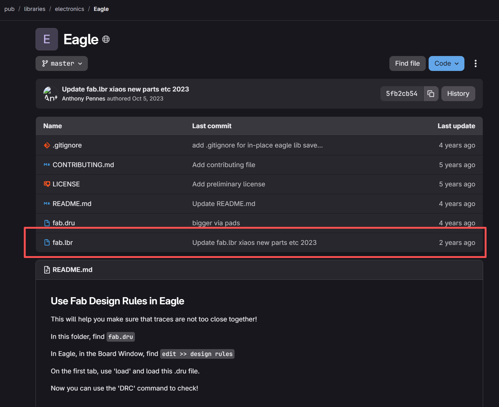
In Fusion 360: 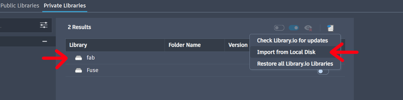
Step 2: Fix the "fab" library to look for component in the right side bar 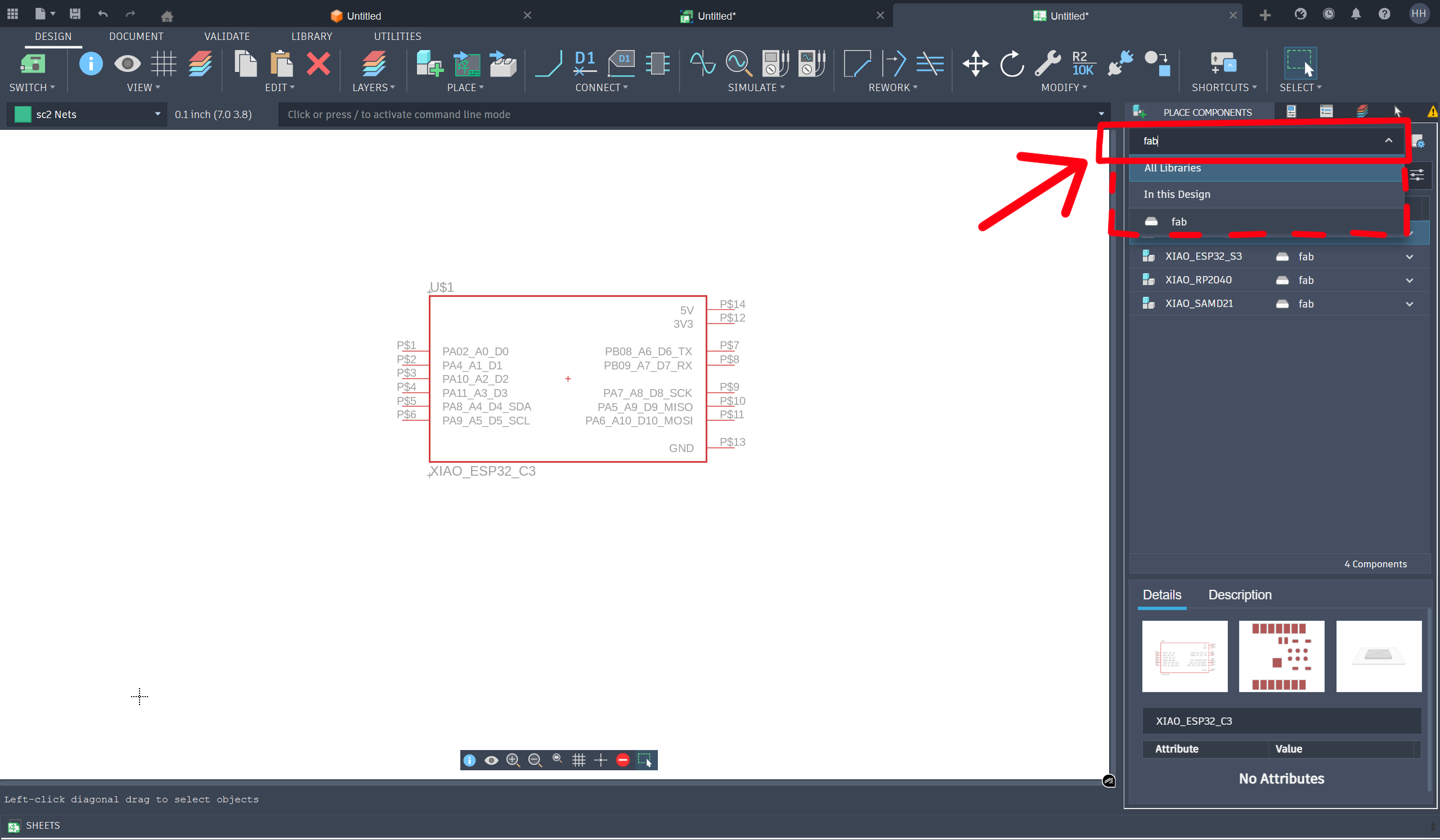
Step 3: Search for the desired component (e.g. XIAO_ESP32_C3, LED, resistor, pinheads) 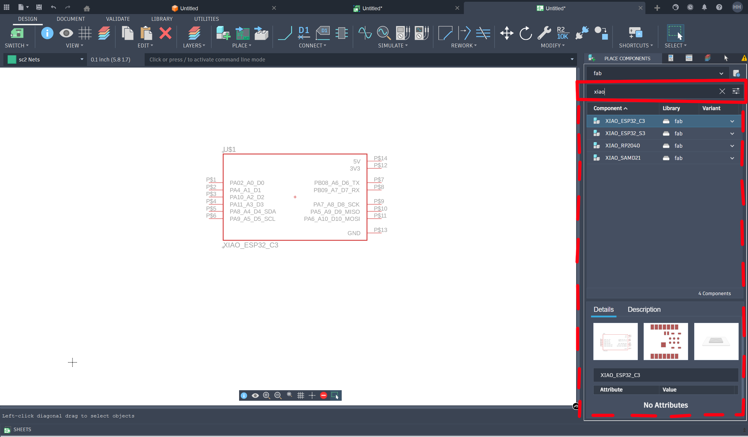
Hardware Specification Analysis
(Refer to the same sub-section from the previous Individual Work #1)
Pin Assignment Plan
Here below is my plan for connecting the pins:
| Pins (IAO-ESP32-C3) | Signal Name |
|---|---|
| A0 | Ultrasonic Sensor TRIG |
| A1 | Ultrasonic Sensor ECHO |
| D7 | Servo PWM |
| D8 | LED + |
| D9 | LED + |
| D10 | LED + |
| GND | LED - / Ultrasonic Sensor / Servo PWM |
| VCC | Ultrasonic Sensor / Servo PWM |
Circuit Design Implementation
Schematic Design
Step 1: Connect components to the micro-controller by using the "Net" tool 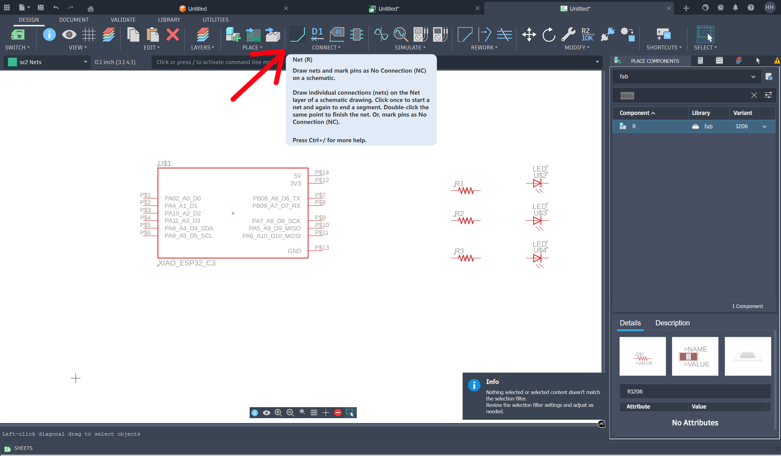
Step 2: Connect the resistors to the LEDs and micro-controller 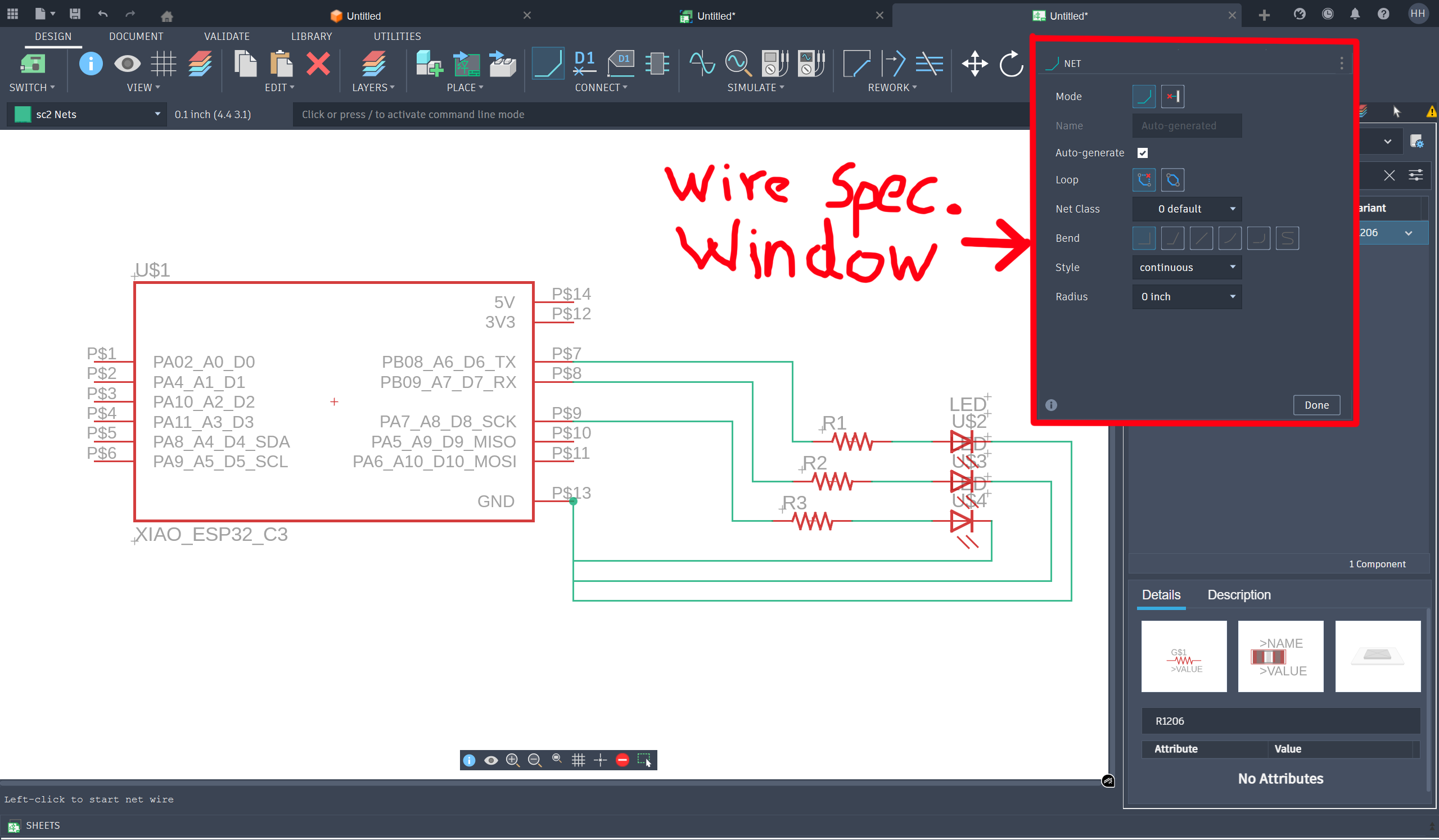
Step 3: Look in the fab library for a 5x2 Pinhead and place it in our schematic design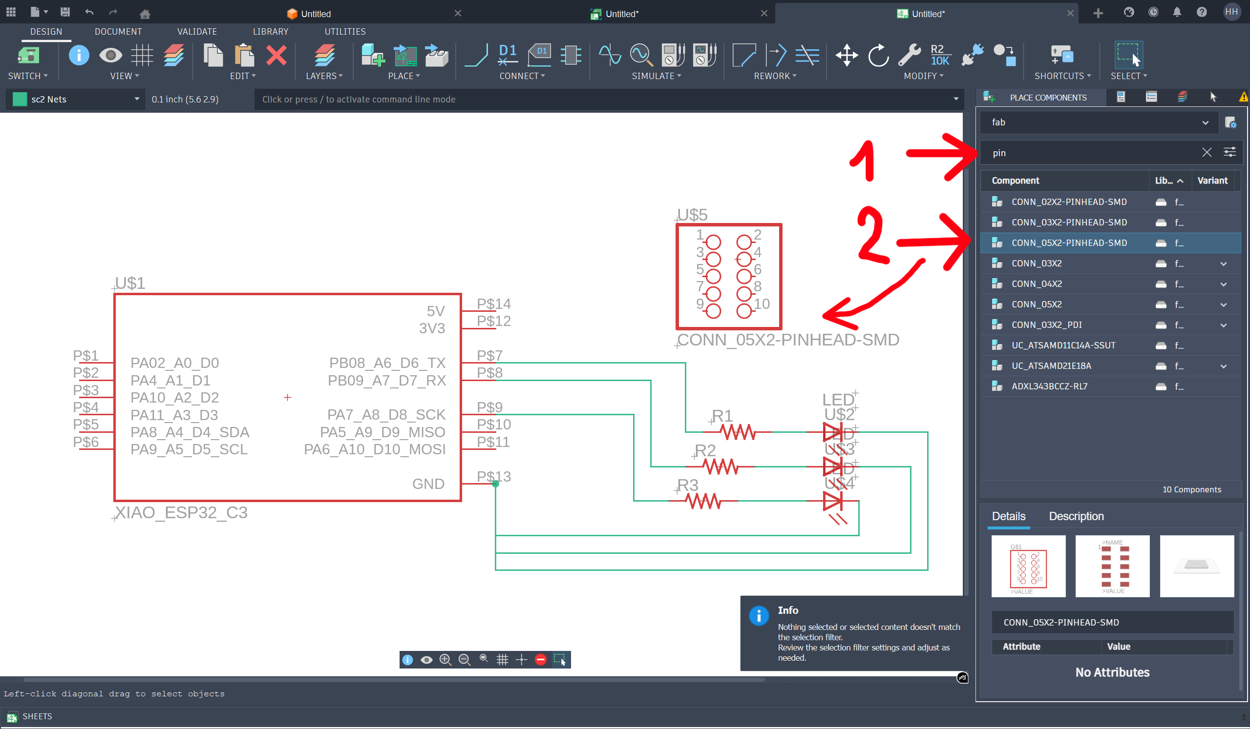
Step 4: Reposition the 5x2 Pinhead to the left of the mricro-controller and connect the 2 components together 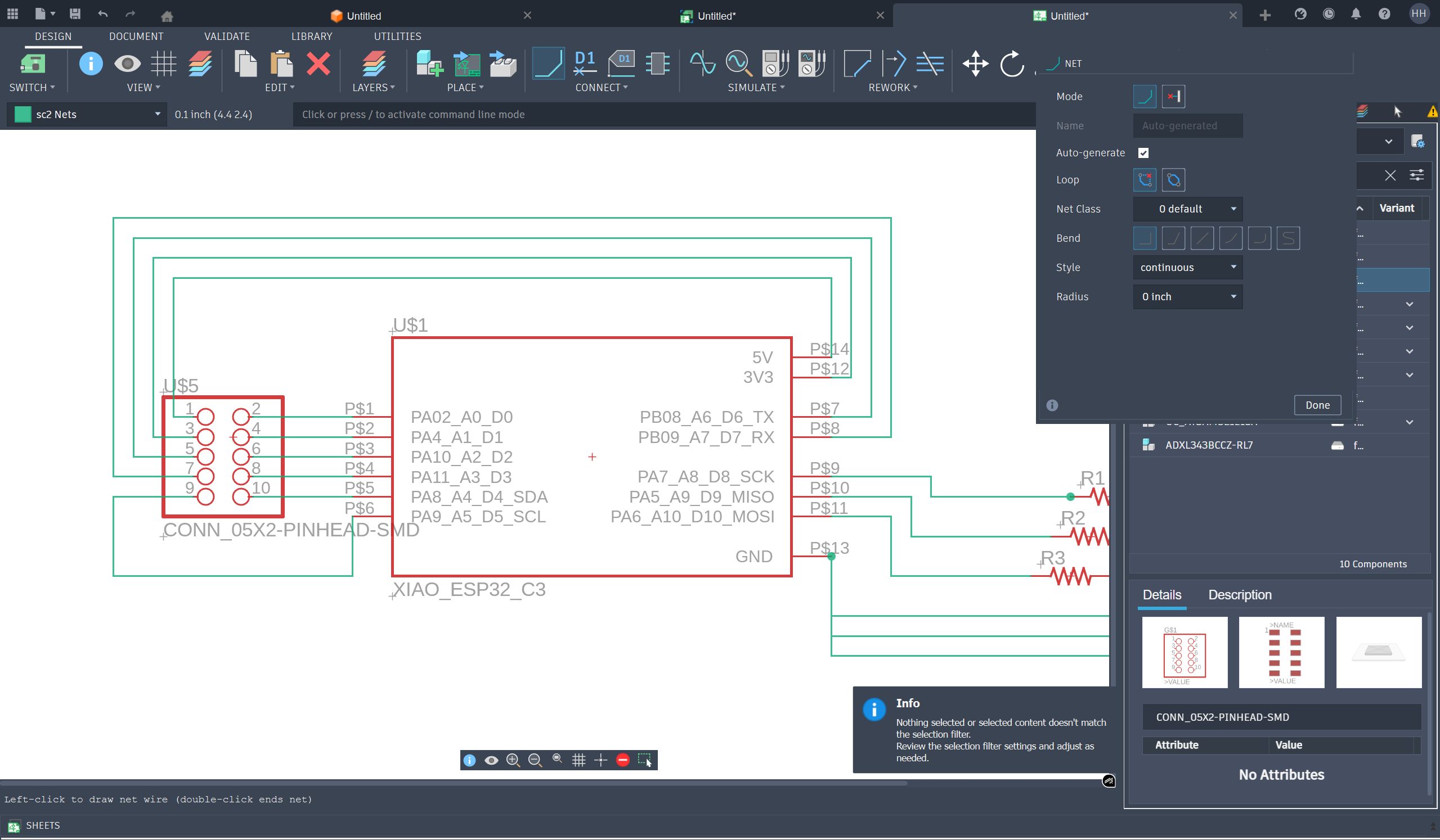
PCB Layout and Design
Step 1: Switch the view to 2d PCB mode (from Schematic mode) 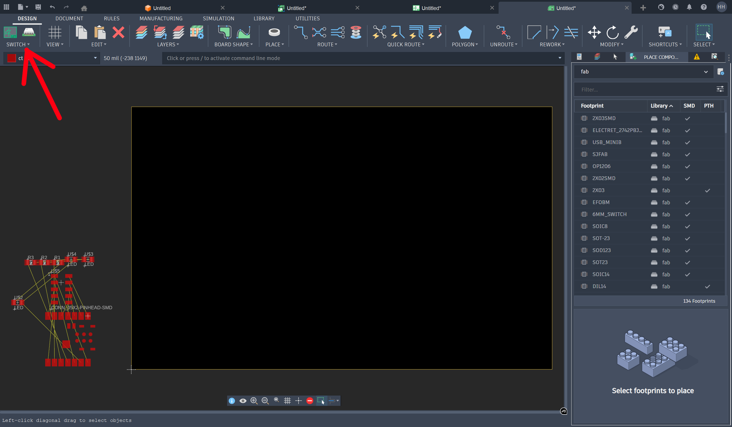
Step 2: Draw the shape of the board... 1st try NOT CREATIVE ENOUGH!!! 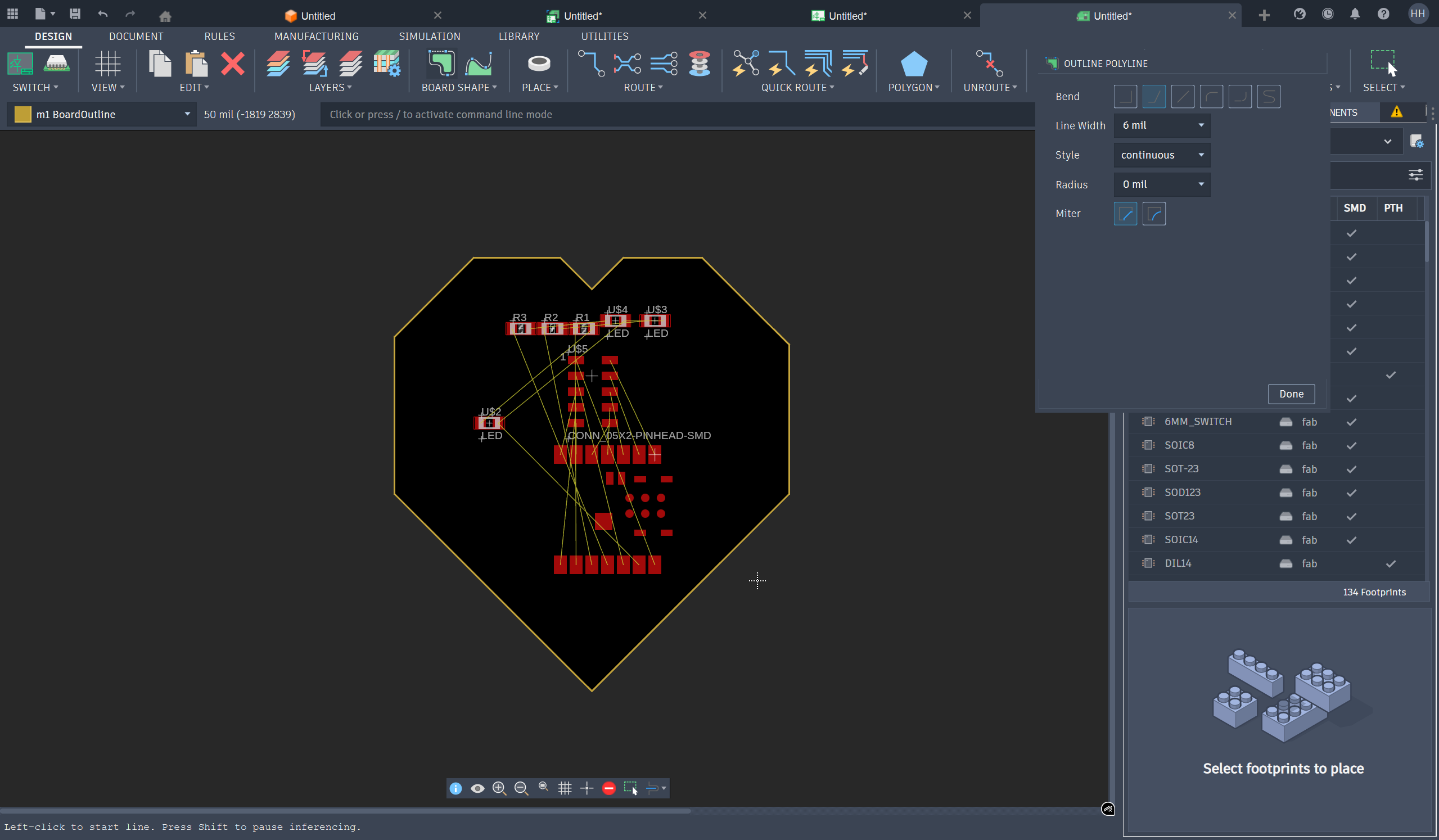
Step 3: 2nd try... Draw the shape of the board using the Outline Polyline and Outline Spline tools - within the BOARD SHAPE tools section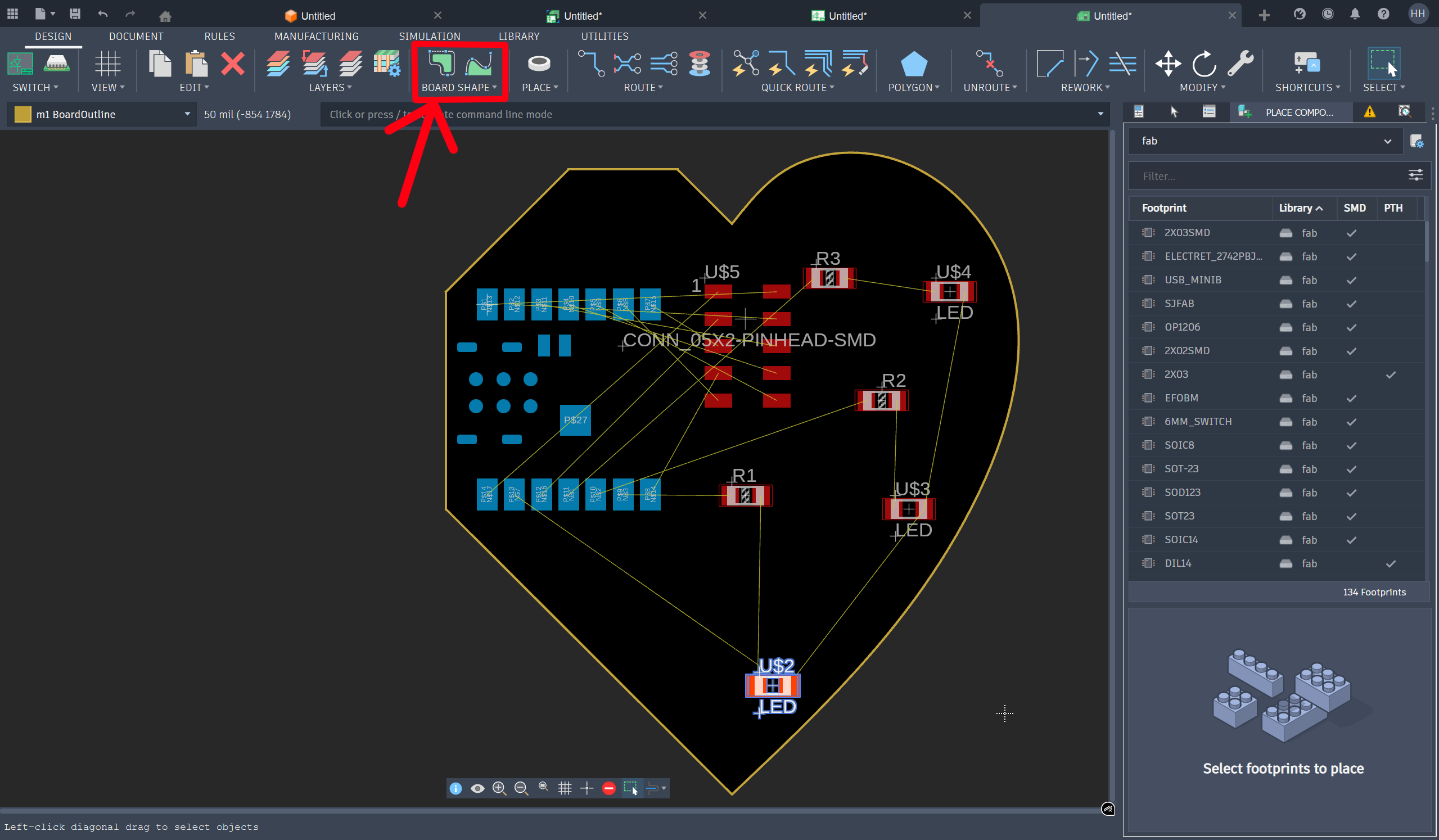
Step 4: Check the Design Rules and adjust them if needed... 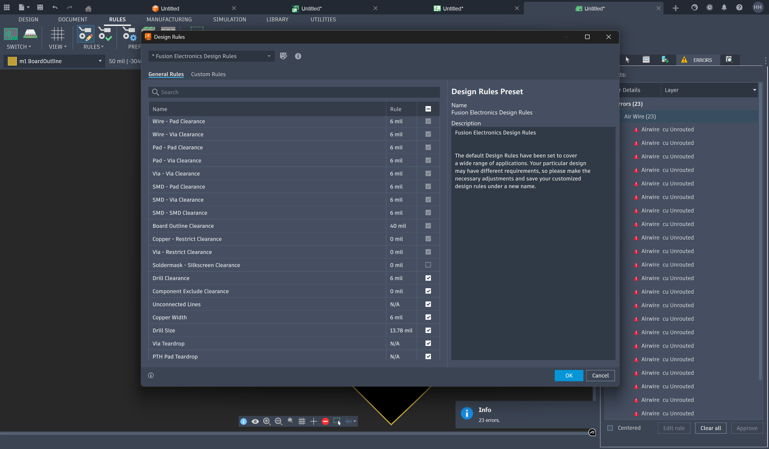
...Adjust some Design Rules parameters from 6 mil to 16 mil according to the capability of our CNC equipment, as shown below: 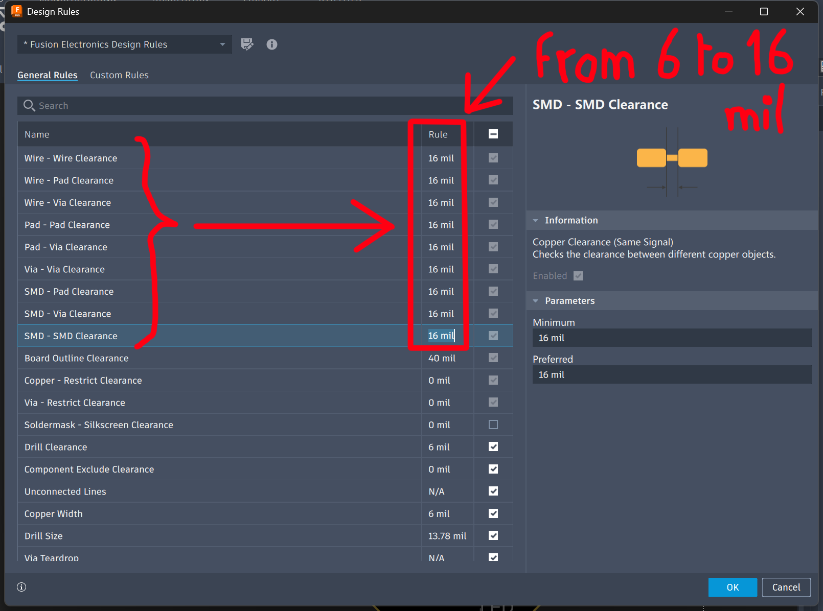
Step 5: Click QUICK ROUTE and then select Autorouter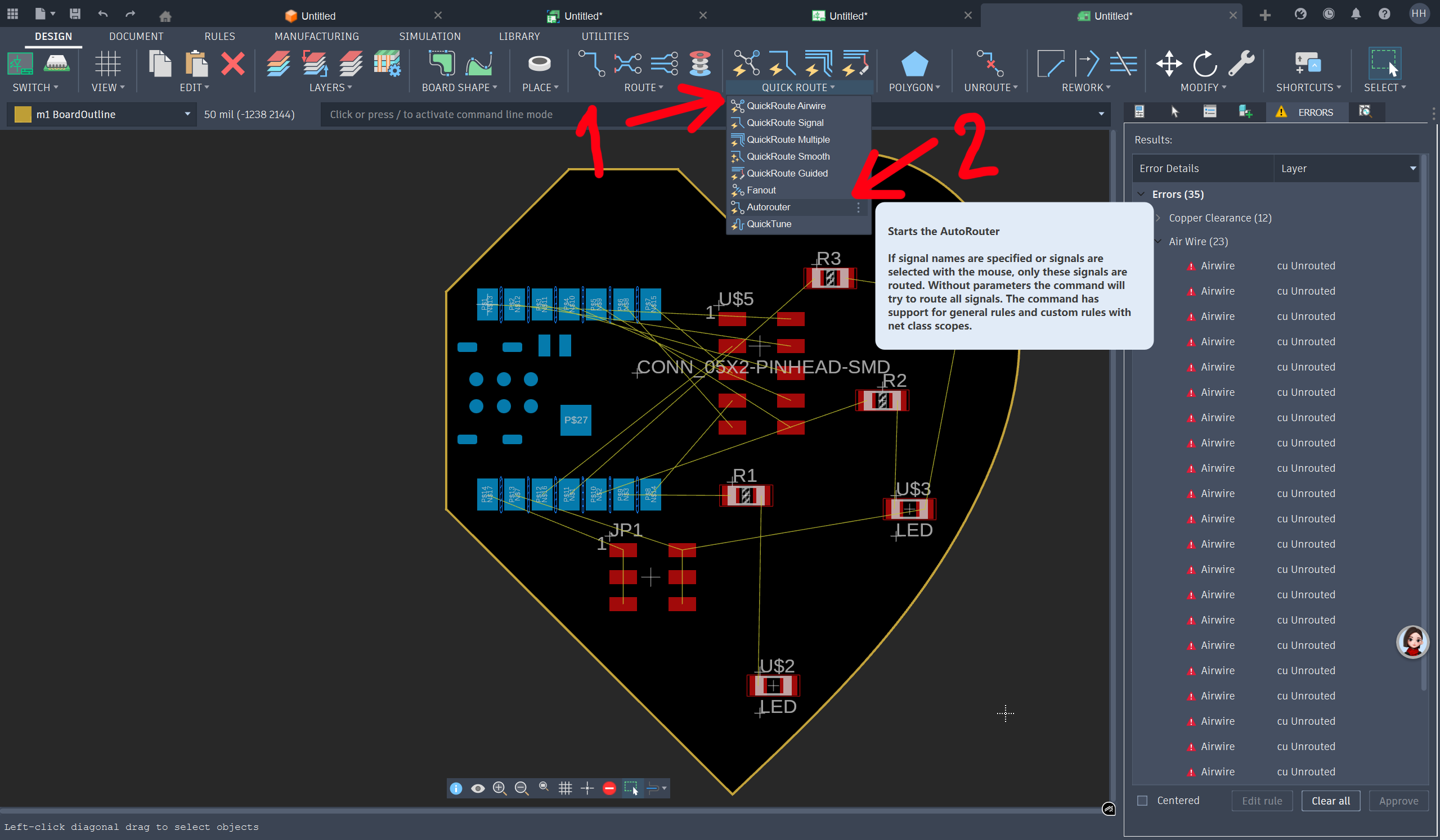
...Check the Main Setup** of the autorounting, and click Continue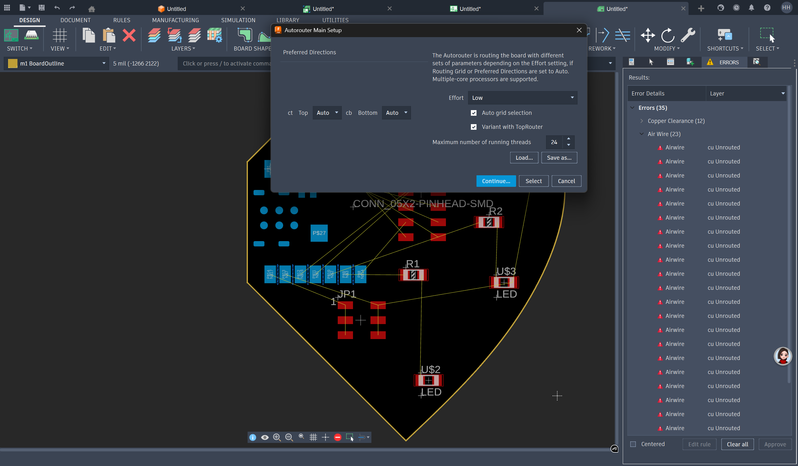
...A dialogue box appears with the Routing Variants... Click Start! 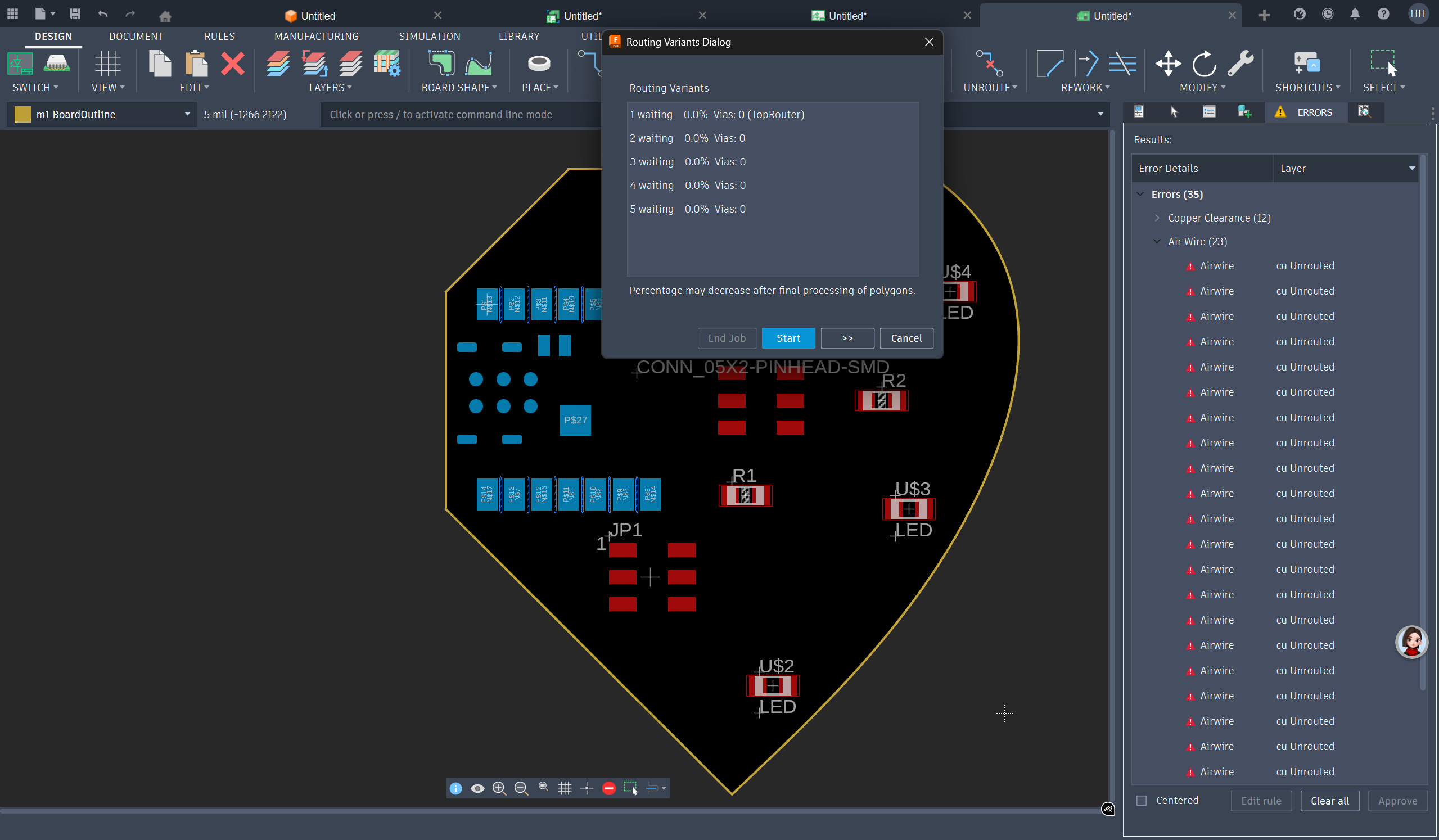
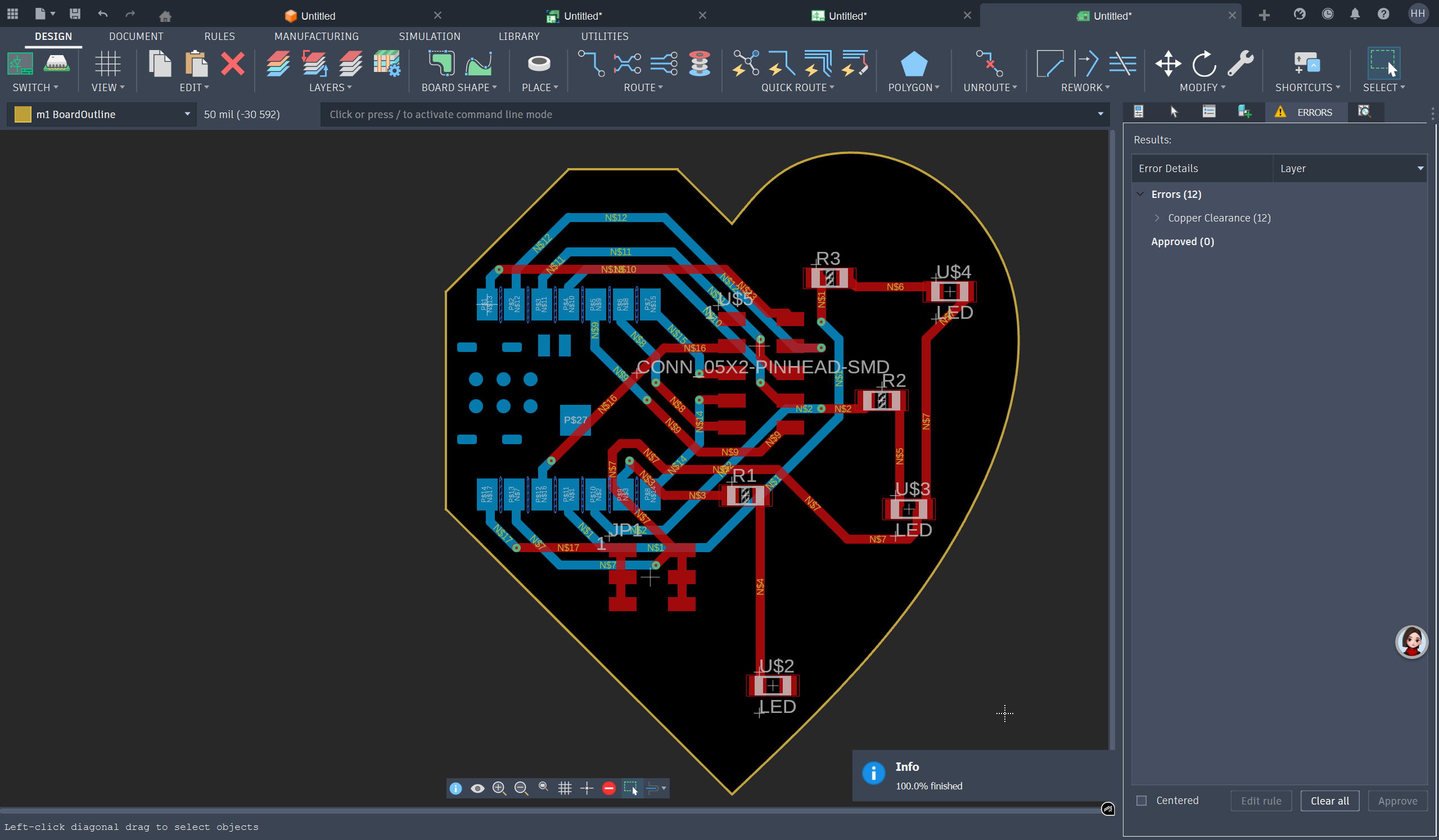
Here is the Auto-Routing result:
- The Routing Top Layer is RED
- The Routing Bottom Layer is BLUE
- There are 12 errors for Copper Clearance in Results Window (right side)
Step 6: Change the Pad - Pad Clearance from 32 mil to 24 mil to adapt the gap between pads of the micro-controller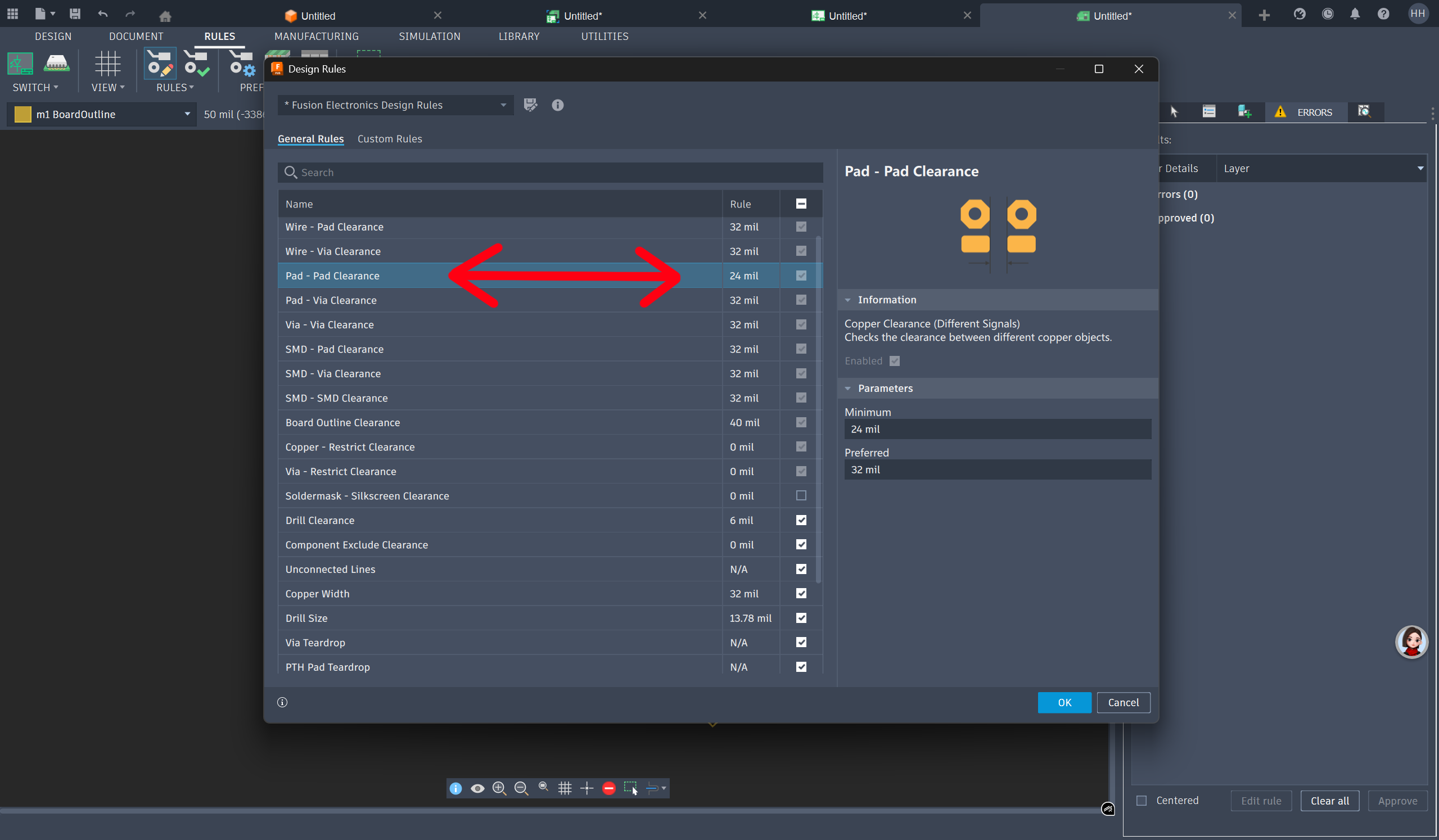
...The Results window show there is no more error, and is therefore ready to push our design to 3D PCB 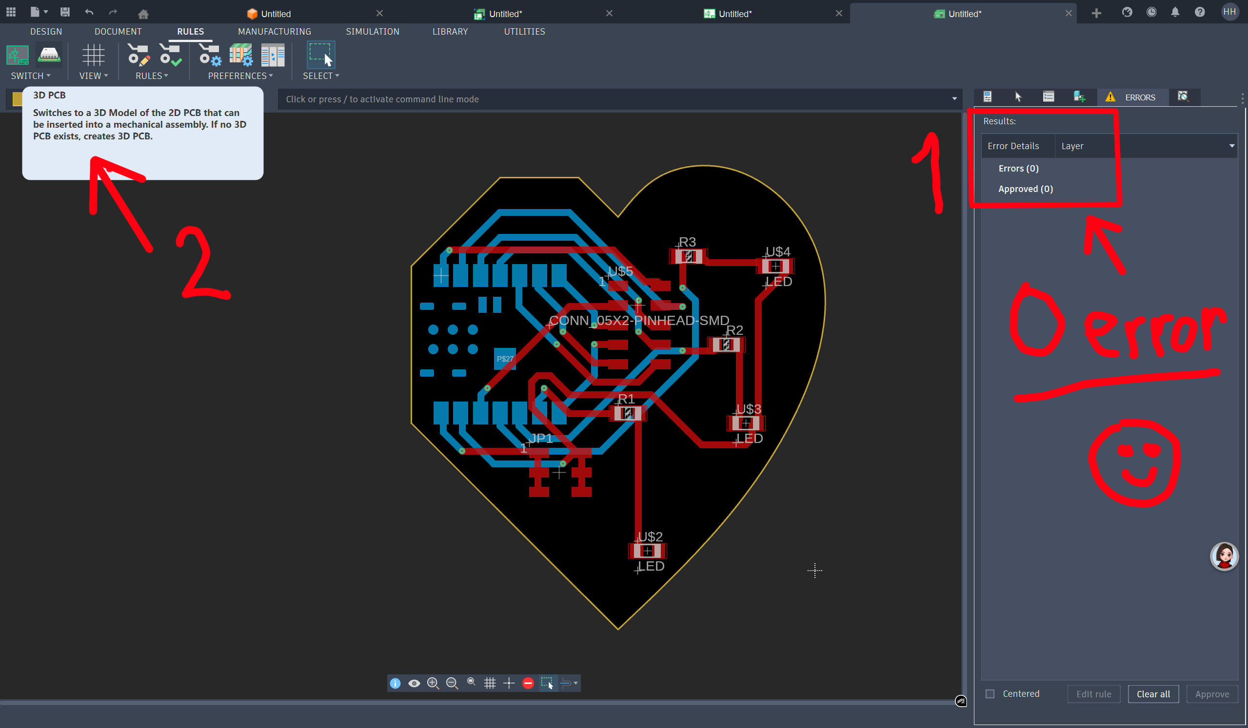
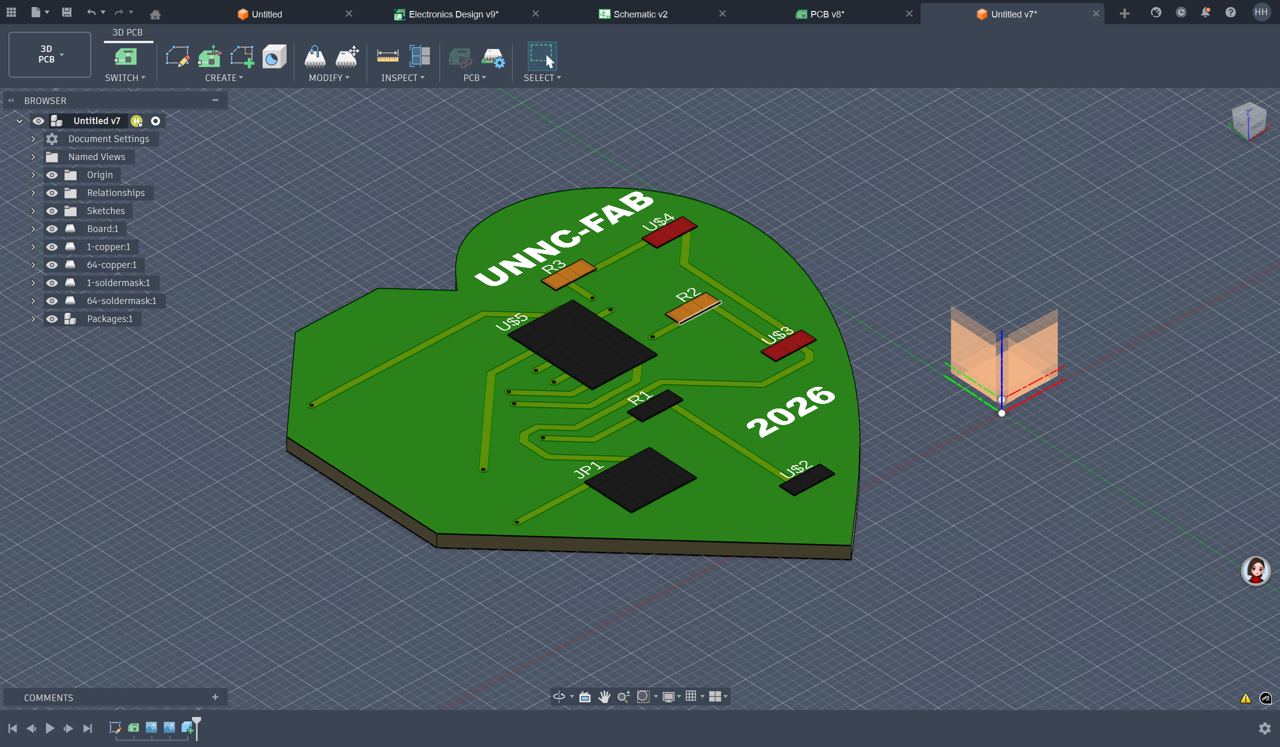
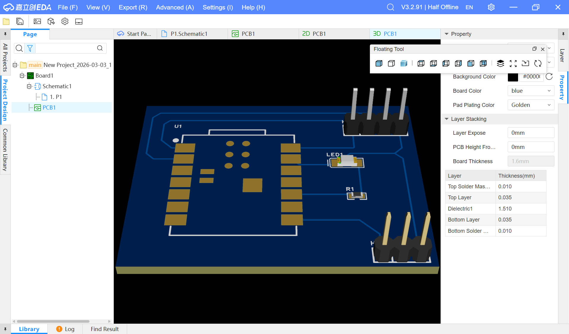
Final PCB Design
3D PCB visualisation
Top face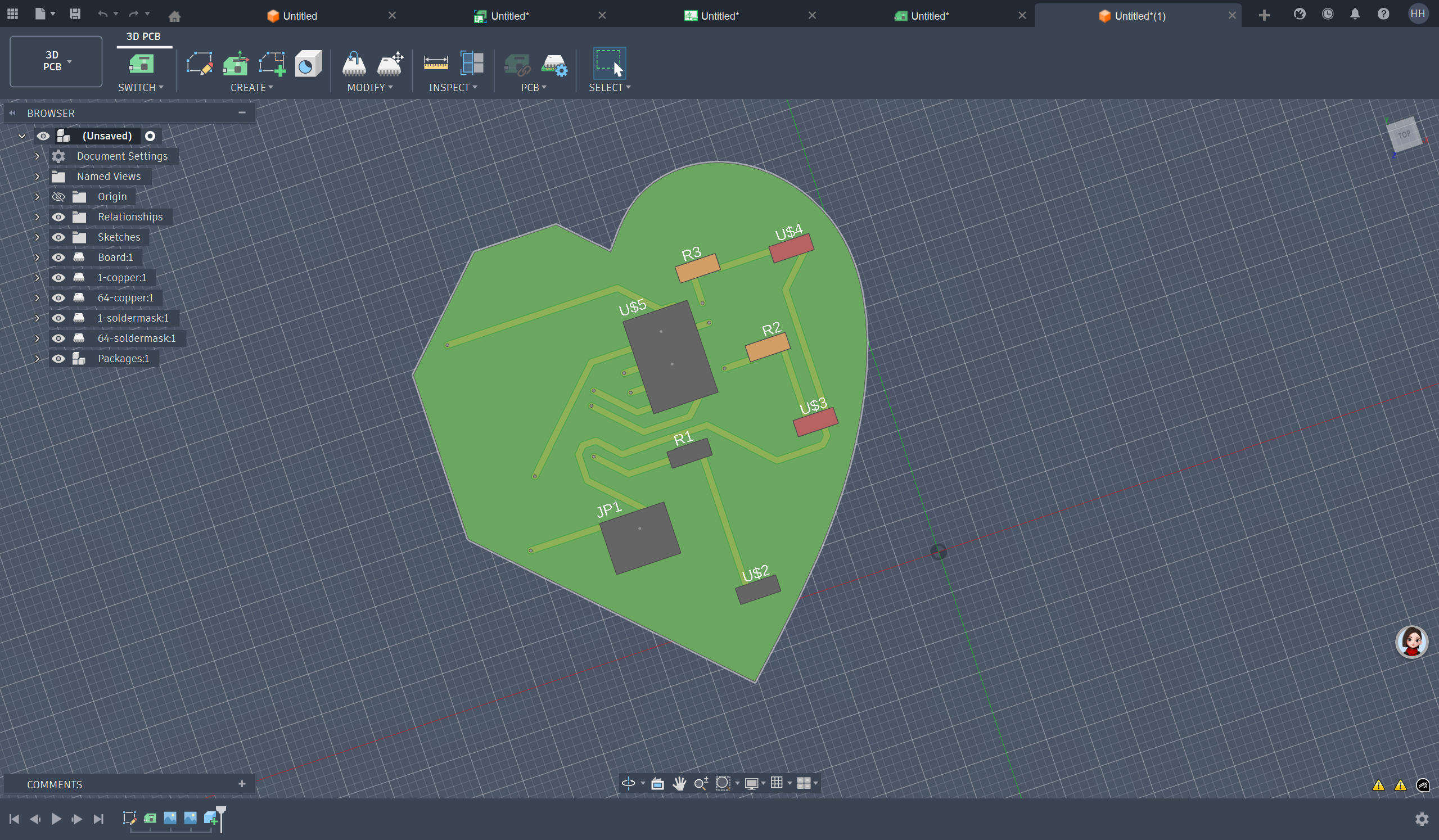
Bottom face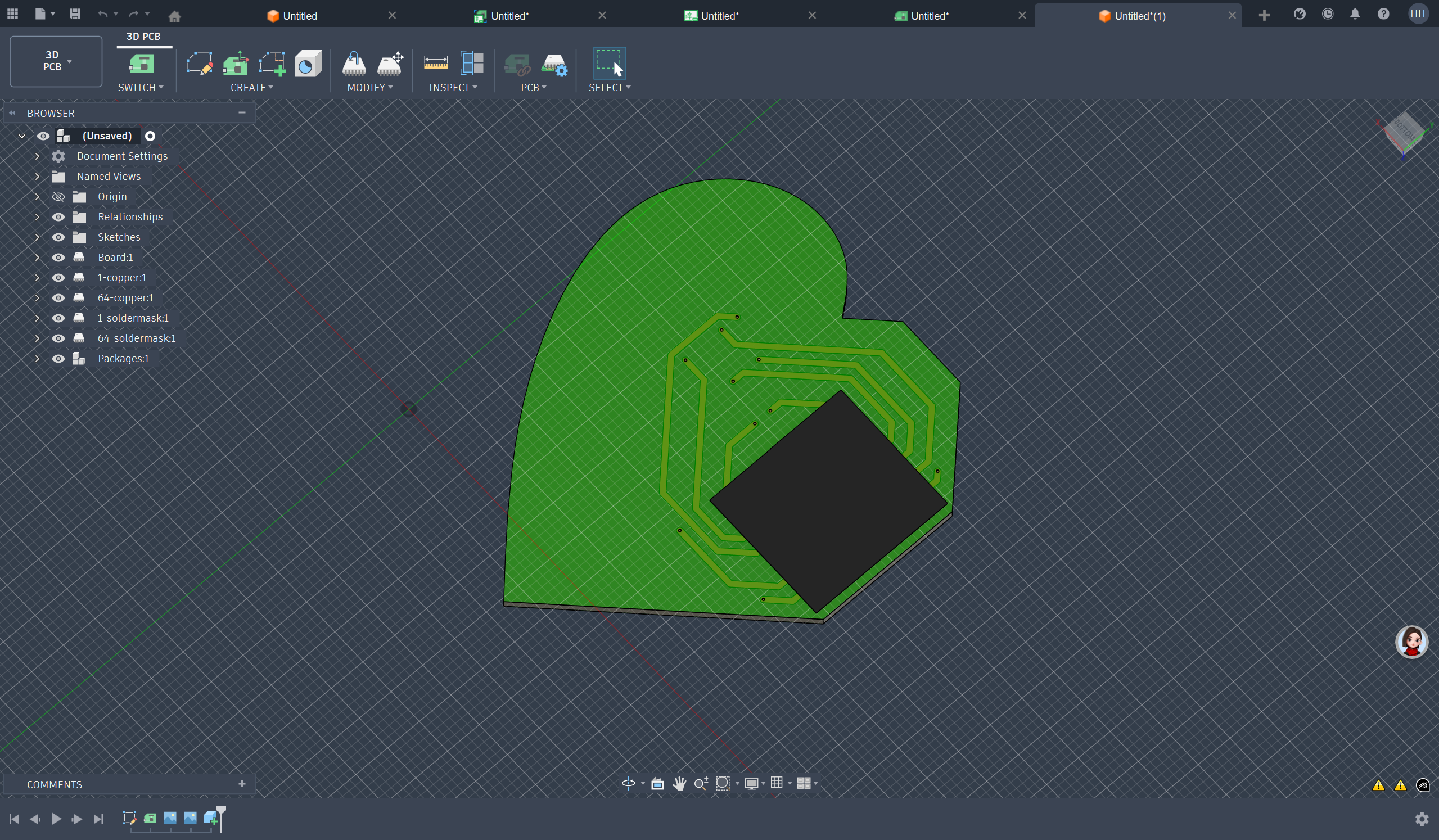
Step 1: Hide the components (folders and layers) to keep visible only the PCB board with the 2 copper layers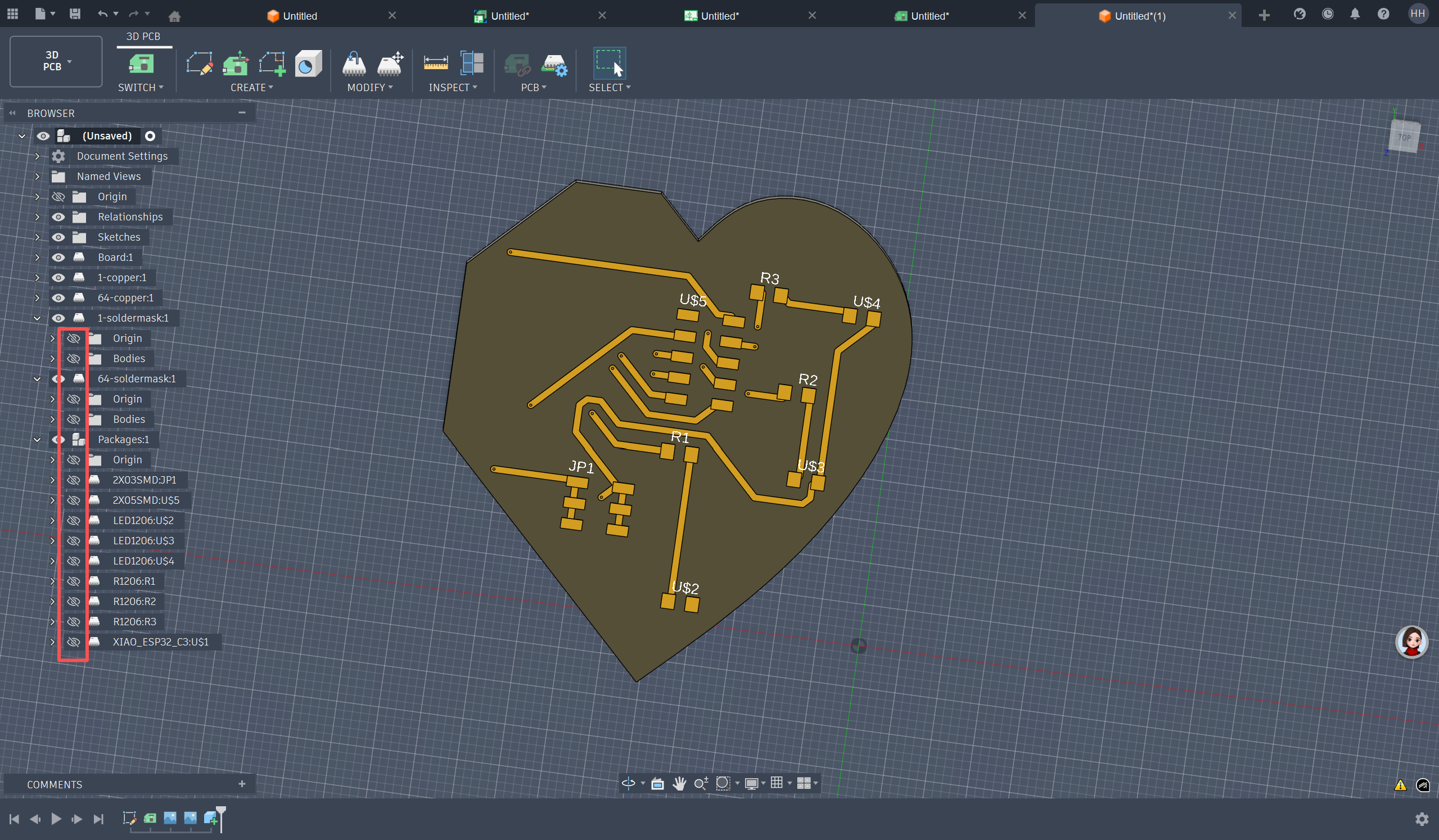
Final Result - Top Face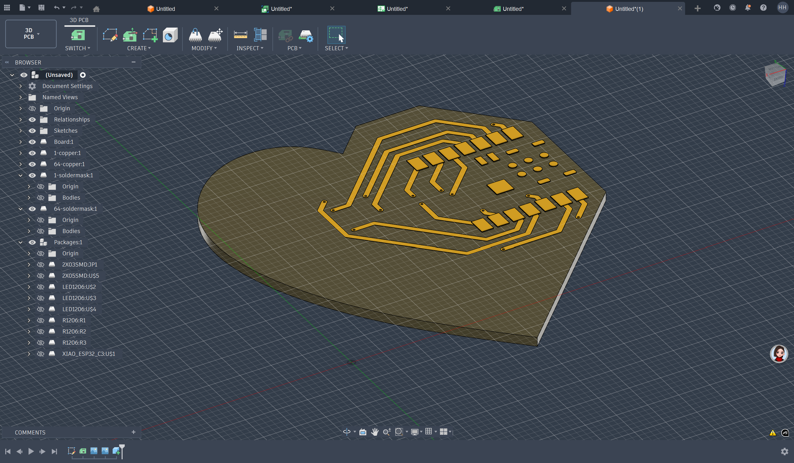
Final Result - Bottom Face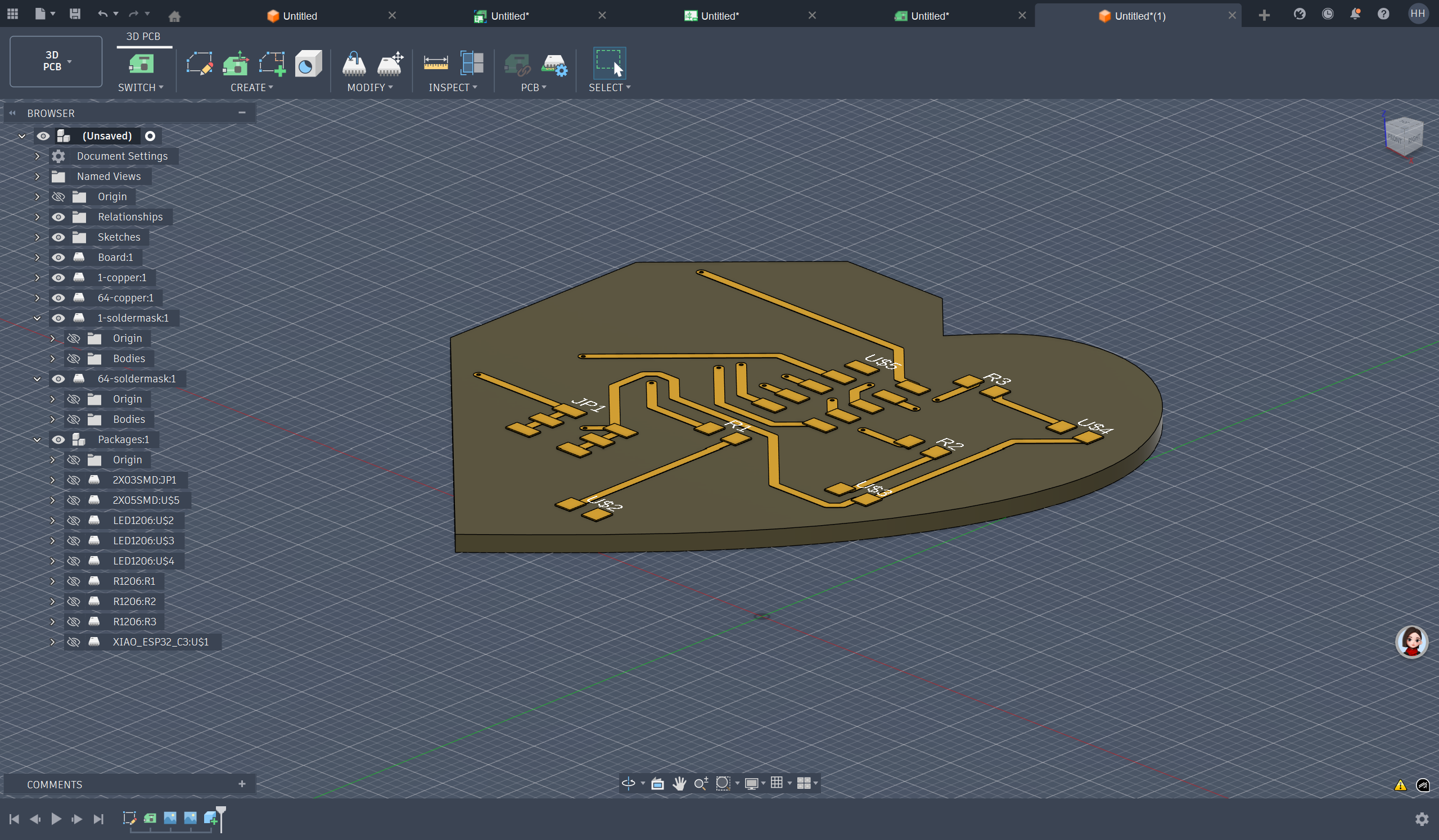
Step 2: LET'S HAVE MORE FUN... Let's try to add some text to be engraved on the board... 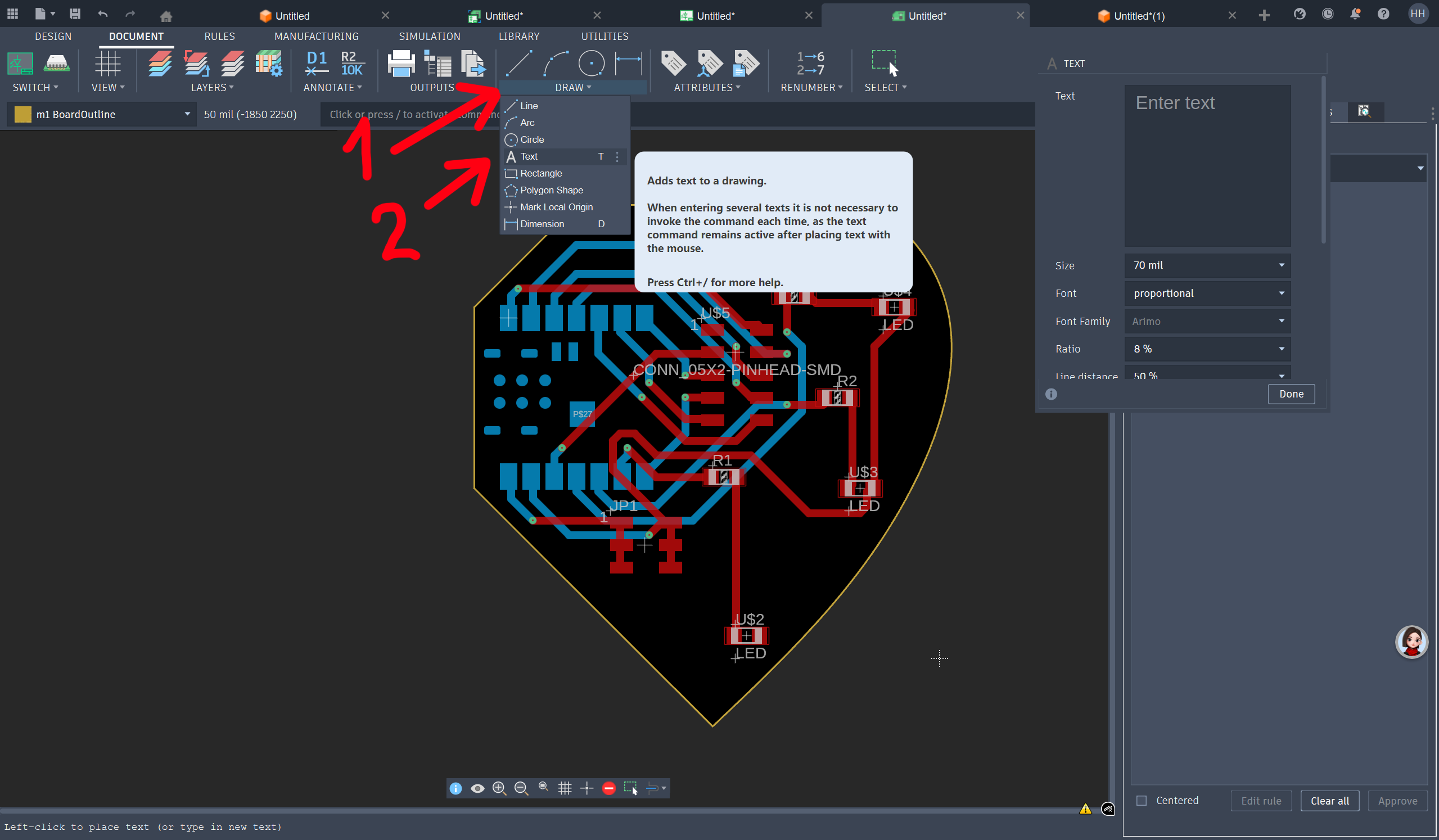
...Enter the text "UNNC-FABLAB 2026" and set/change the parameters if needed... Click Done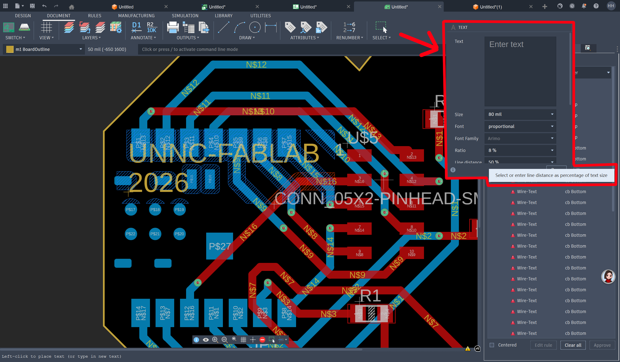
Here is the result: 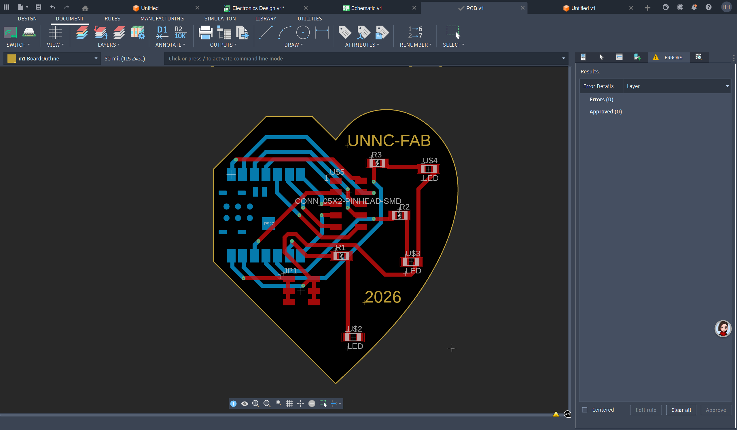
...Let's change the Typface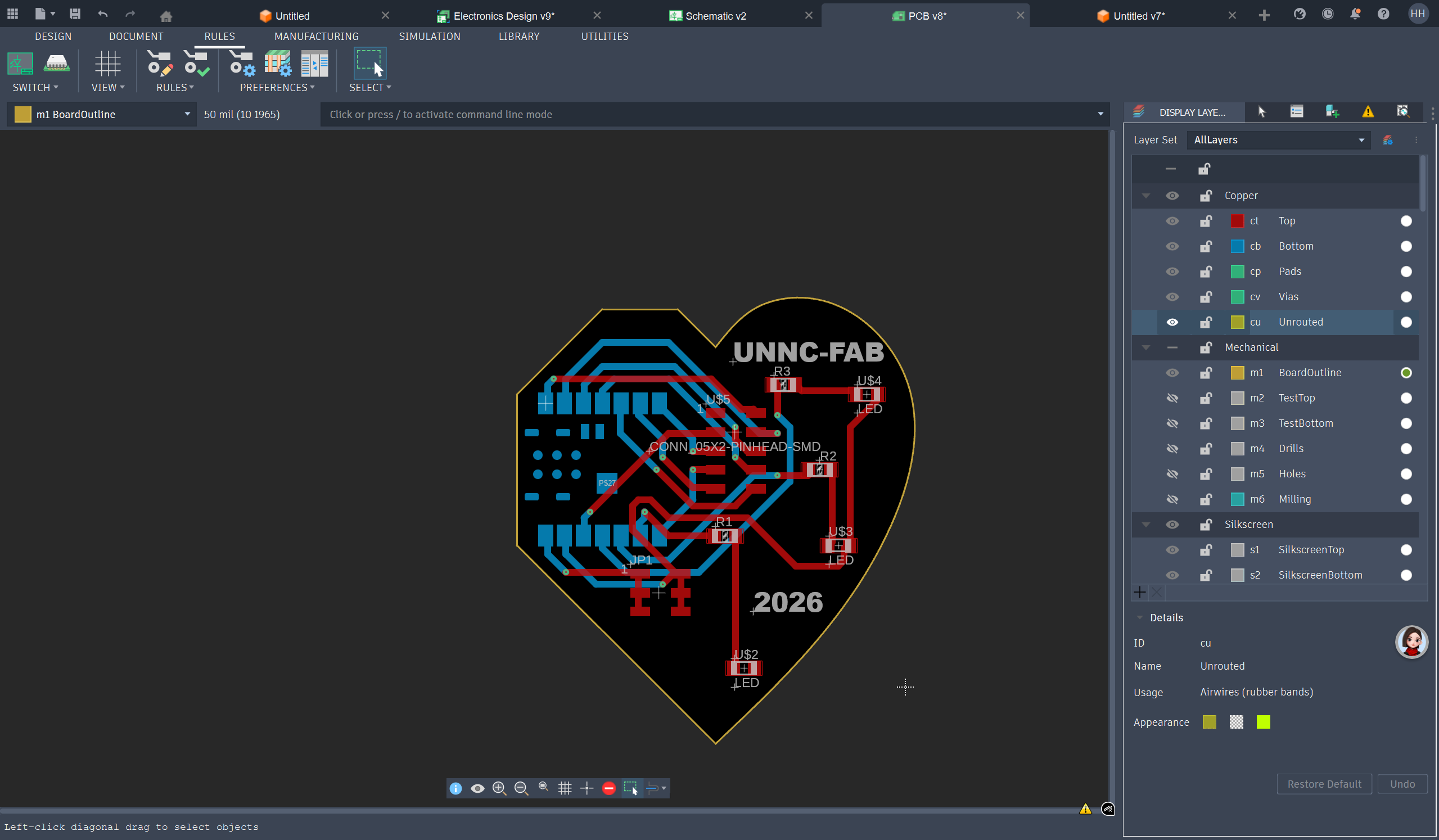
Step 3: Select the text and right click. Set the Layer property to "s3 NamesTop"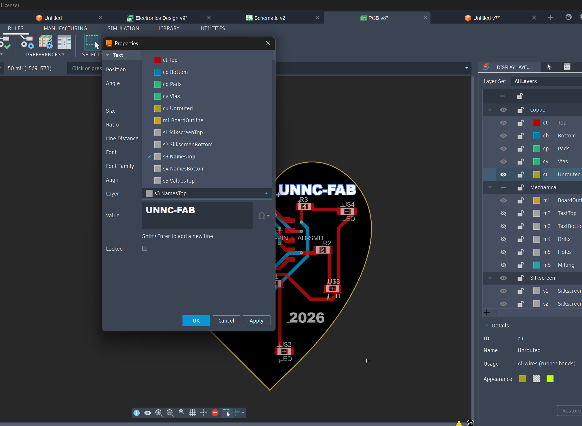
Final 3D PCB with engraved text on top face