Prior knowledge
|
I already made some PCBs manually years ago but the old way, which is chemically, with UV light and having to dip the PCB in a chemical solution. Other than that, I usually ask for another department at the university I work at to make my prototype PCBs. |
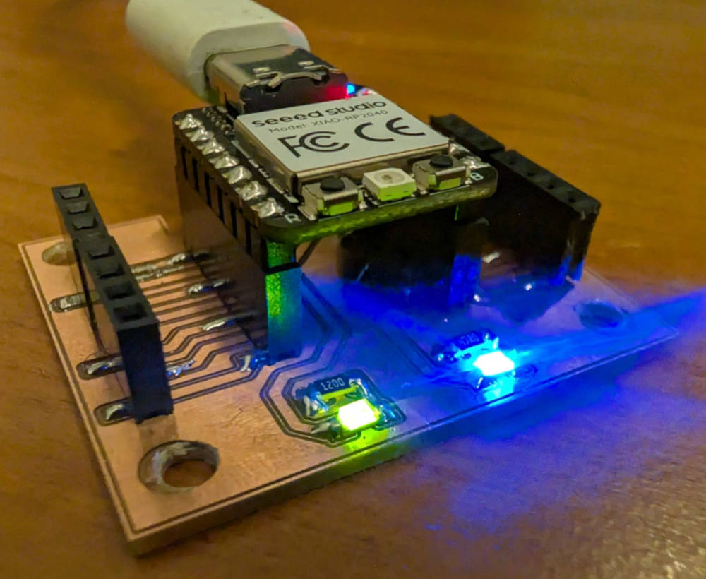
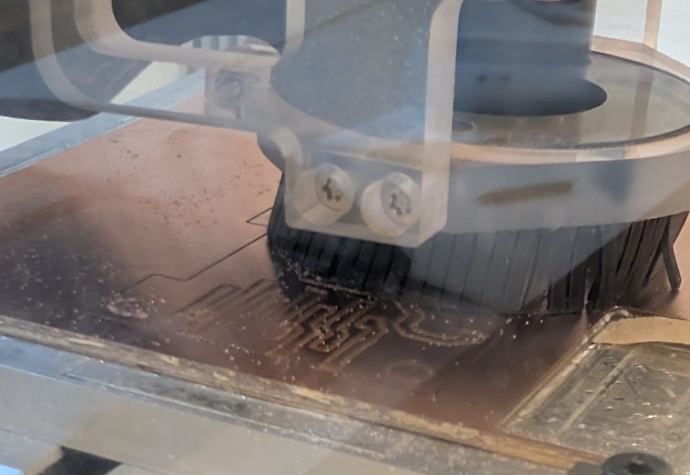
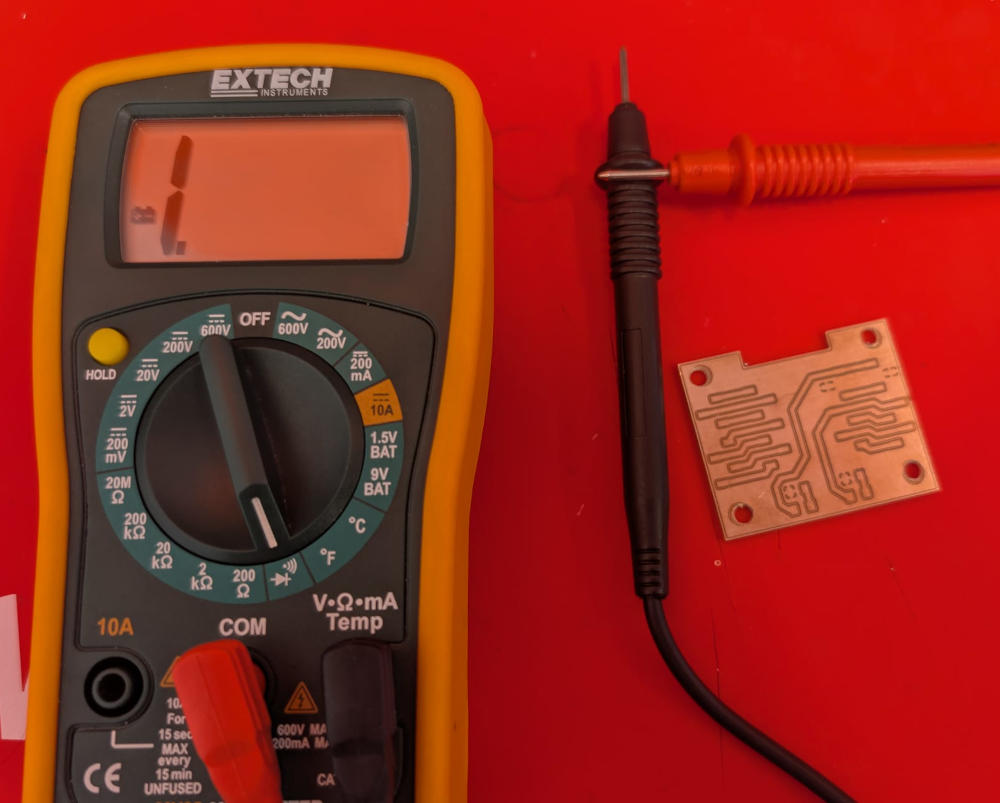
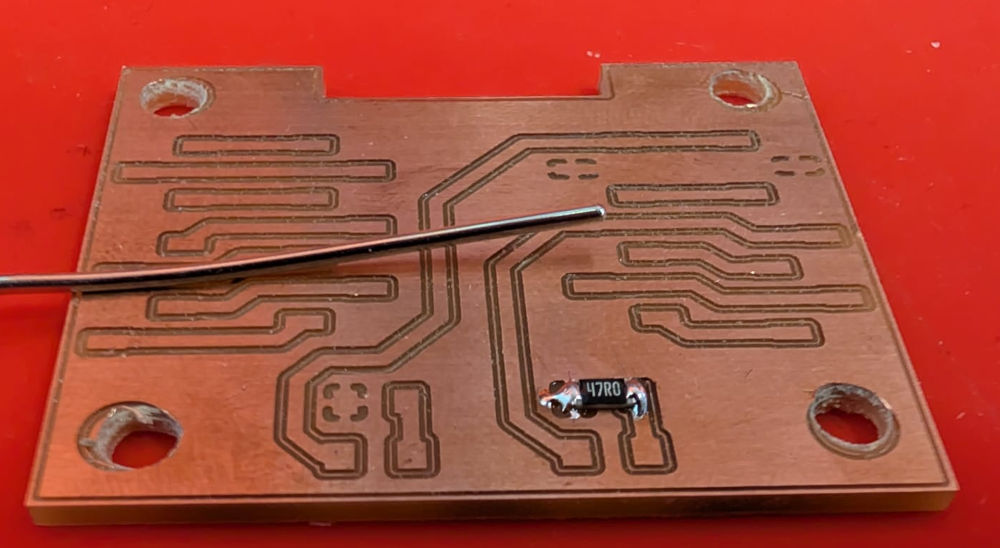
Hero shot
Making a PCB with a PCB milling machine
The FabLab ULB possesses 2 different models :
-
OM1004 by Bantam (software : Bantam Tools)
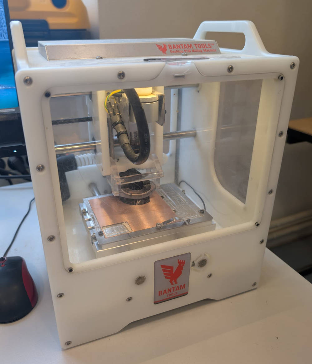
Efficient and easy to use.
-
4MILL300ATC by Mipec (software : TrackMaker)
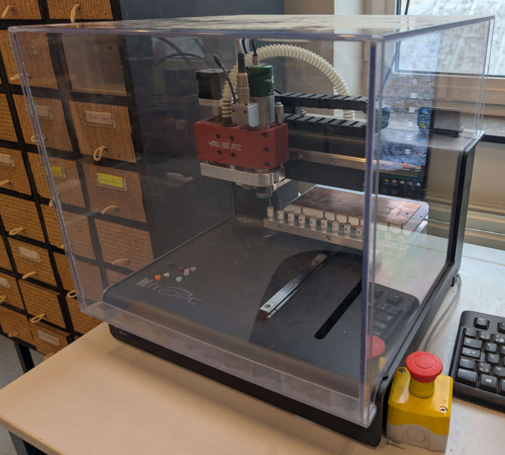
Has an Automatic tool changer (needs pressure).
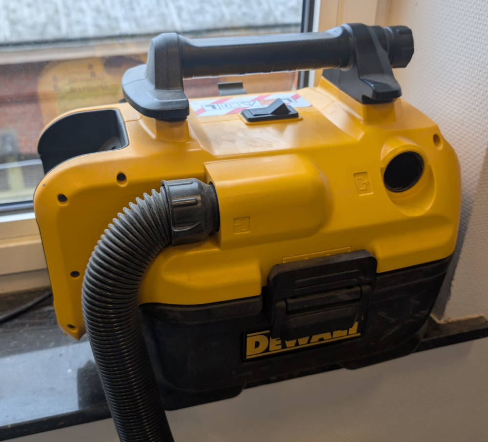
The machines also have a vacuum cleaner connected to it to vacuum the milled bits as well as integrated securities in case of opened window/case.
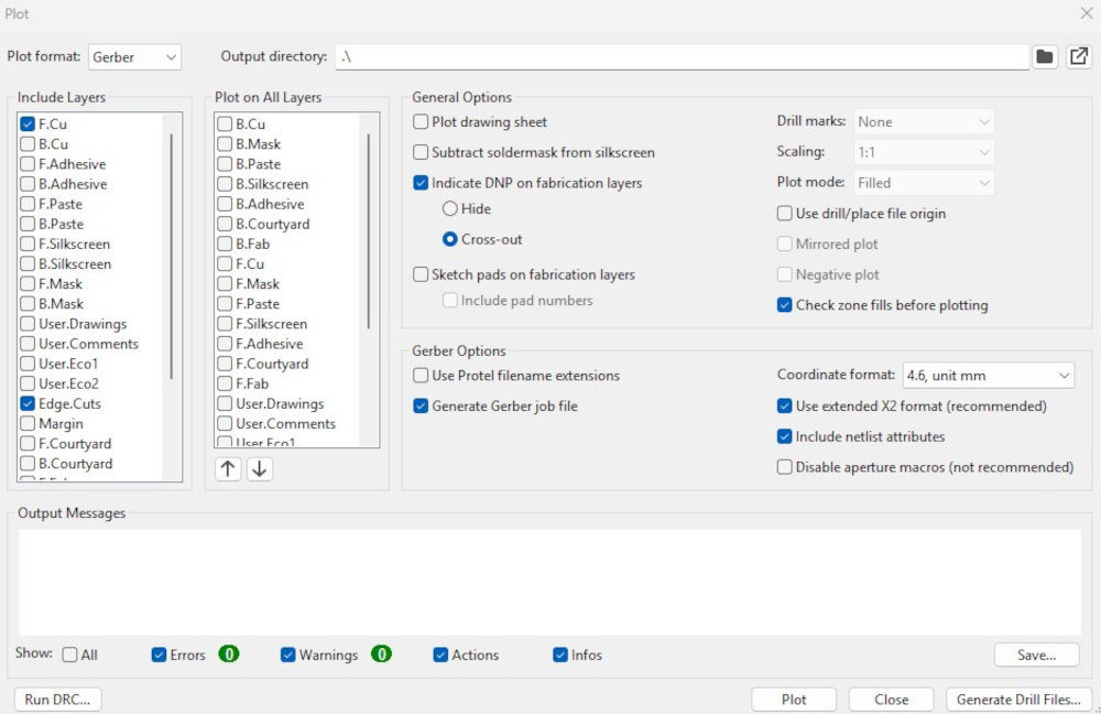
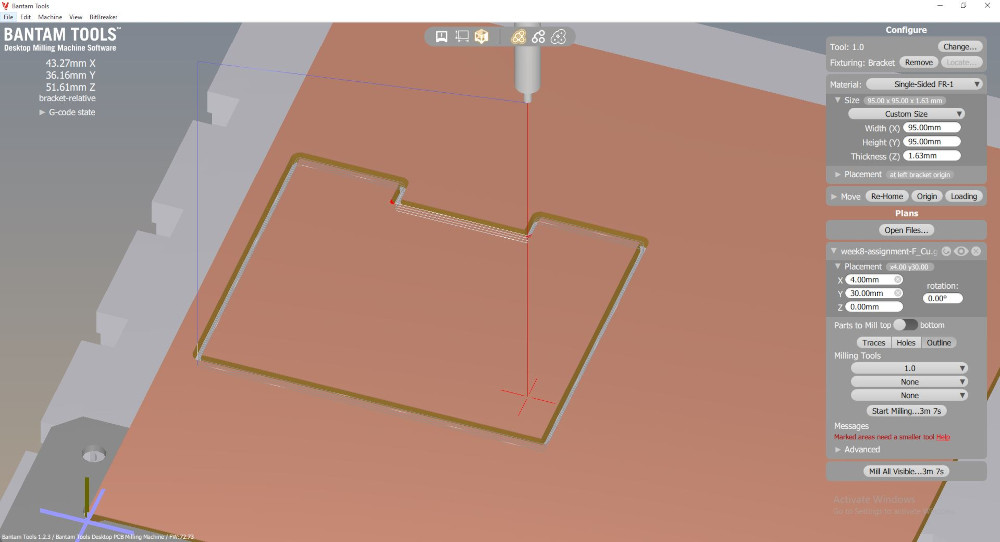
I'll try the Bantam first, before using the machine, I need the fabrication files to work with. For that, I go to KiCad and export the useful Gerber files (go to File, then Fabrication Outputs and select Gerbers(.gbr)...).
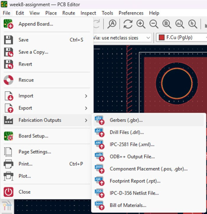
In this case, I check the front/top and edge layers of the PCB. The rest is left by default.
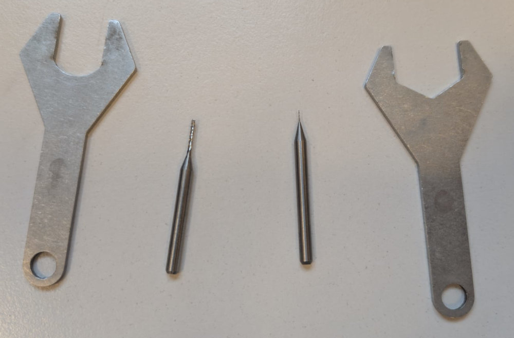
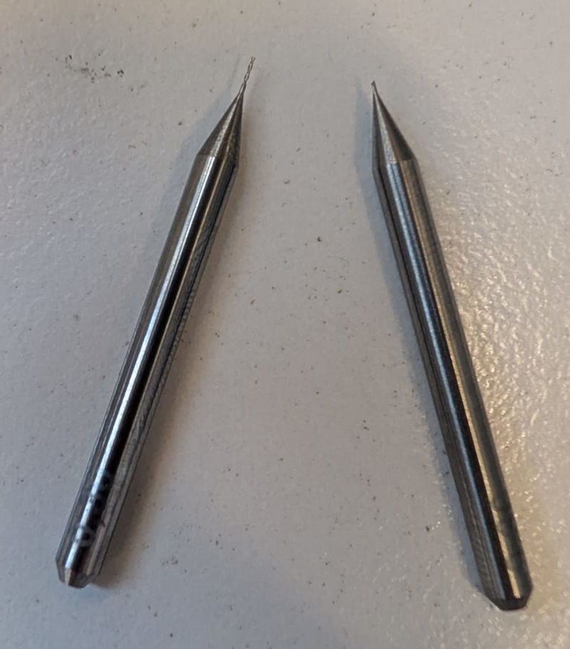
I'll work with a 0,3mm end mill for the tracks and a 1mm end mill for the edge.
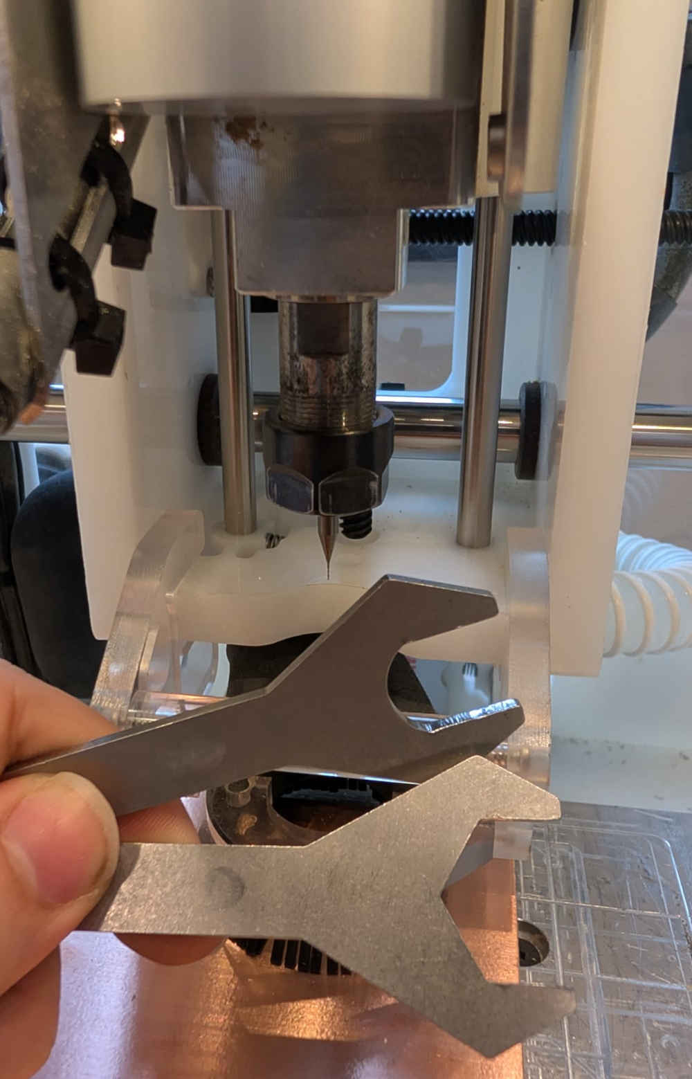
The Bantam comes with wrenches to assemble the end mills with the collet.
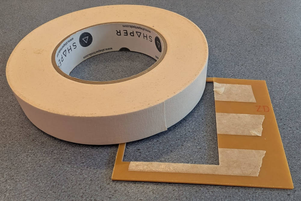
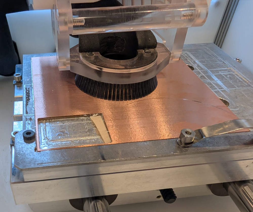
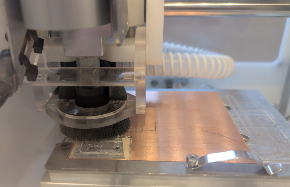
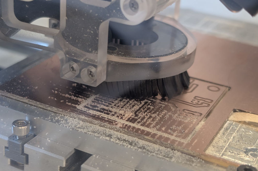
To start, I have to cut the board (I use a FR2 board) and use double sided tape to stick the board to the bottom left of the bed, above the bracket.
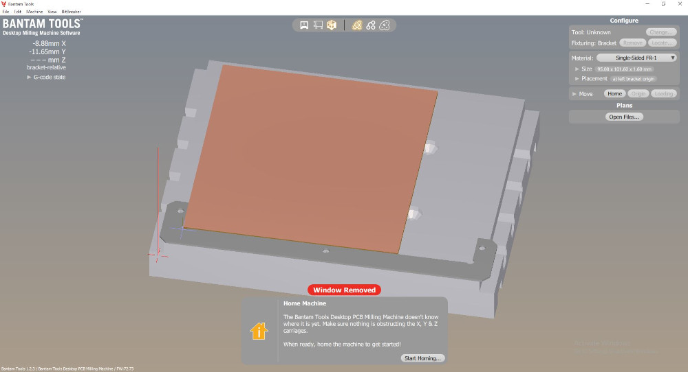
When turning the machine ON and opening Bantam Tools, the software asks me to do an automatic machine homing.
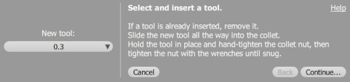
To change end mills, I have to press Change... under Configure.
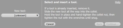
I select the end mill I will use, here since I start with the tracks, I choose the 0,3mm end mill and press Continue....
Then I have to move the tool above the bed (not above the board) and press Locate Tool....
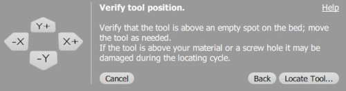
Our end mill is now ready.
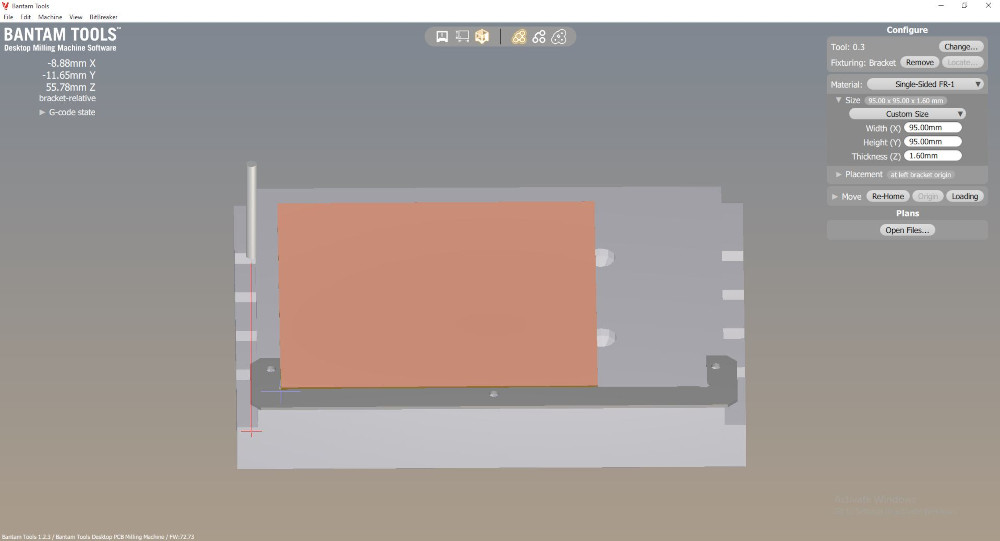
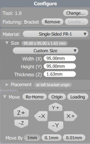
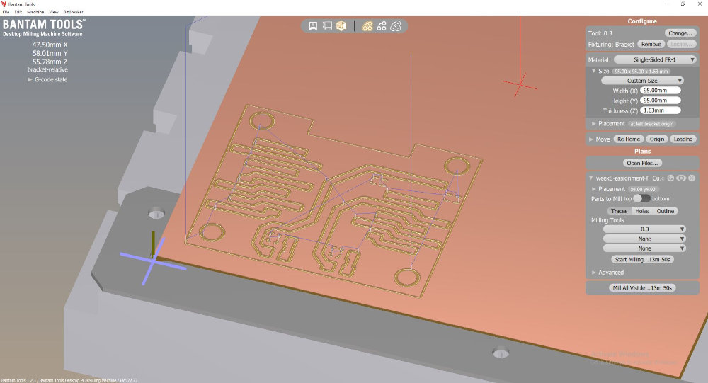
I can now type the size of my PCB in the Material tab.
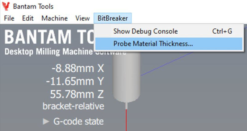
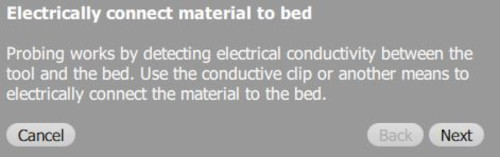
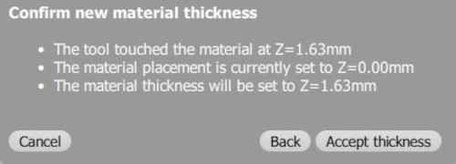
To determine the height of my PCB, I press BitBreaker in the top bar and select Probe Material Thickness....
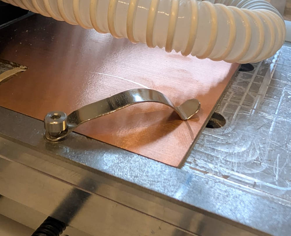
I then have to put the probe on top of the board.
Then, I move the tool above the board and press Probe material....
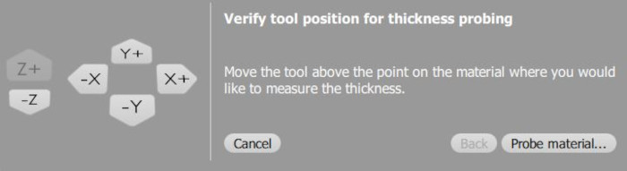
This will give us a measured thickness, i simply have to select Accept thickness. If needed, I can also type it manually.
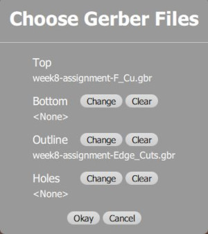
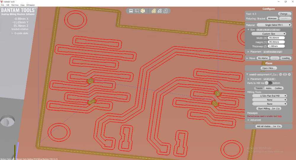
I can now import my 2 gerber by pressing Open Files under Plans and put them in the correct place : front/top layer for Top and edge layer for Outline then press Okay.
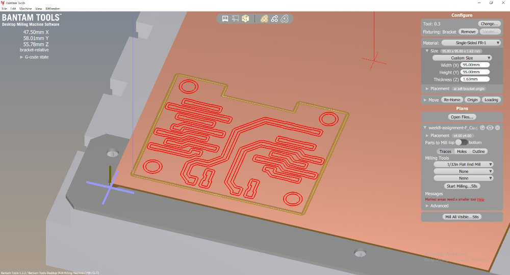
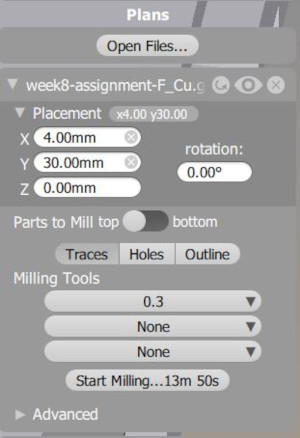
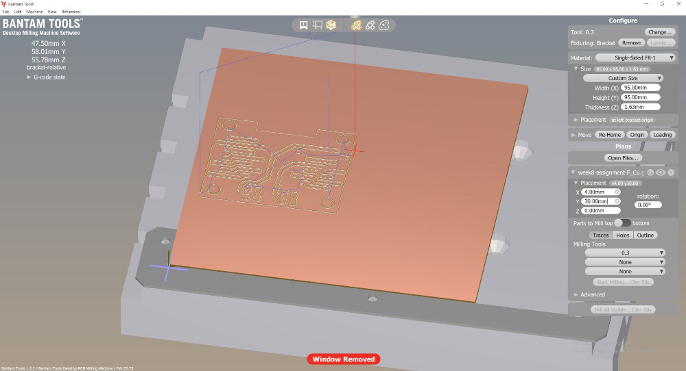
Then under Plans, I have to check Traces only, select the correct end mill and change the location of my PCB by pressing Placement and entering correct values because the board already has a hole due to Jonas using the machine before me.
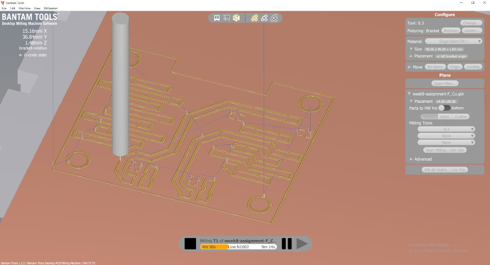
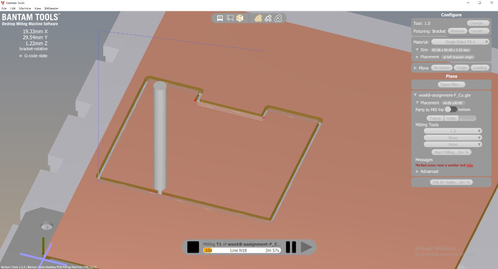
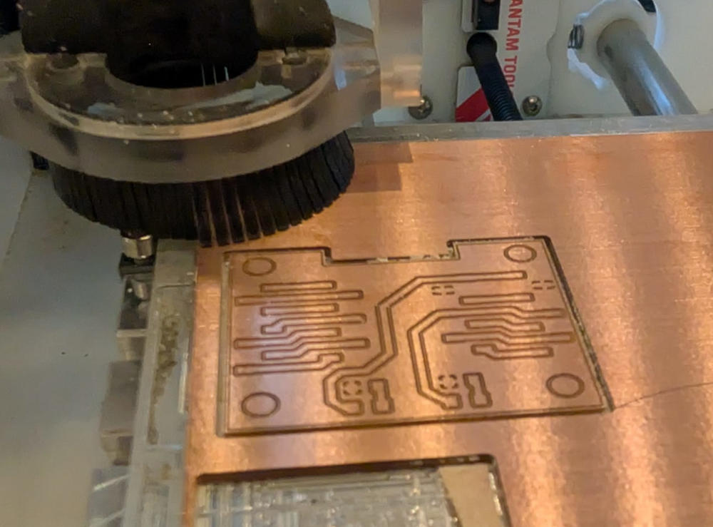
Finally I can press Start Milling... to mill the tracks.
The software also simulates the work at the same time.
Now for the edge, I change the tool to a 1mm end mill for a faster work, redo the Change... configuration and under Plans, I have to check Outline only.
Again, I have to press Start Milling... to mill the edge.
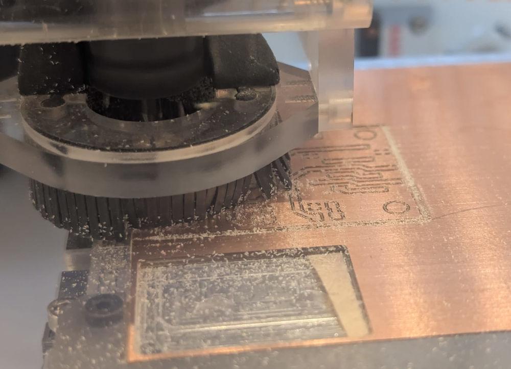
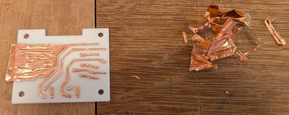
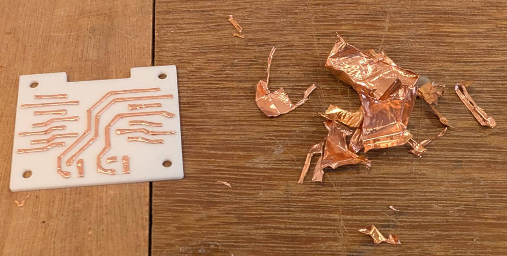
I use a screwdriver to take off my PCB because a bit of the double sided tape under sticks it to the bed.
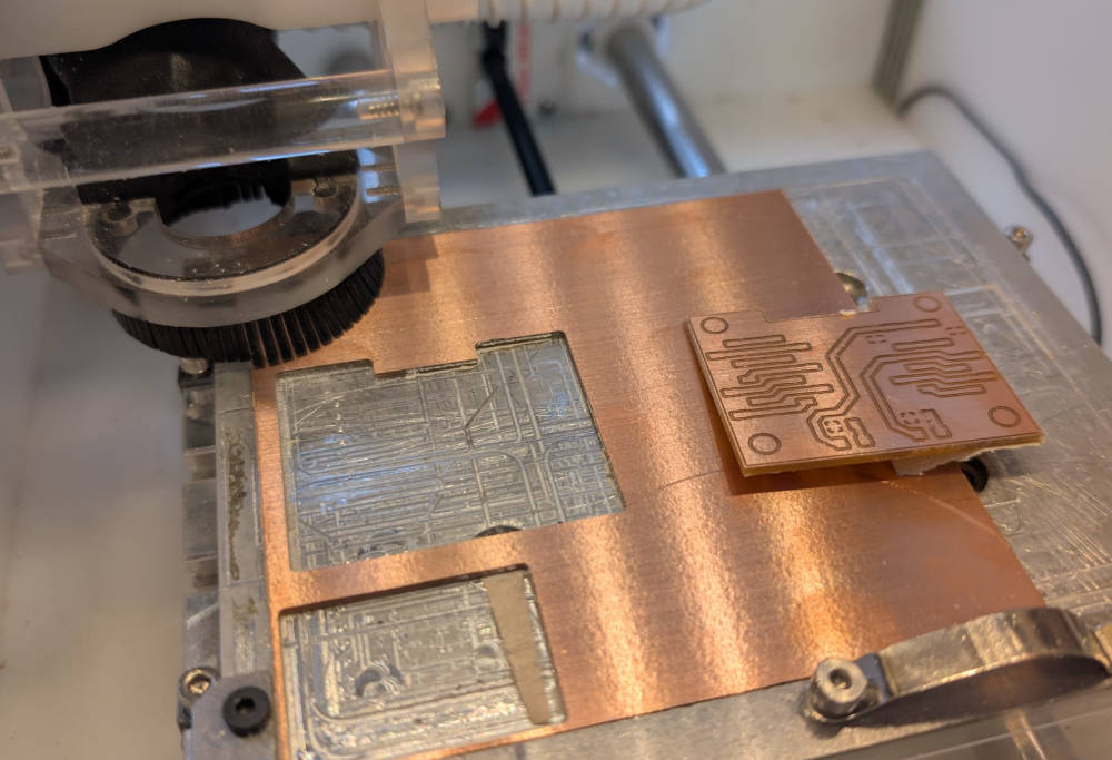
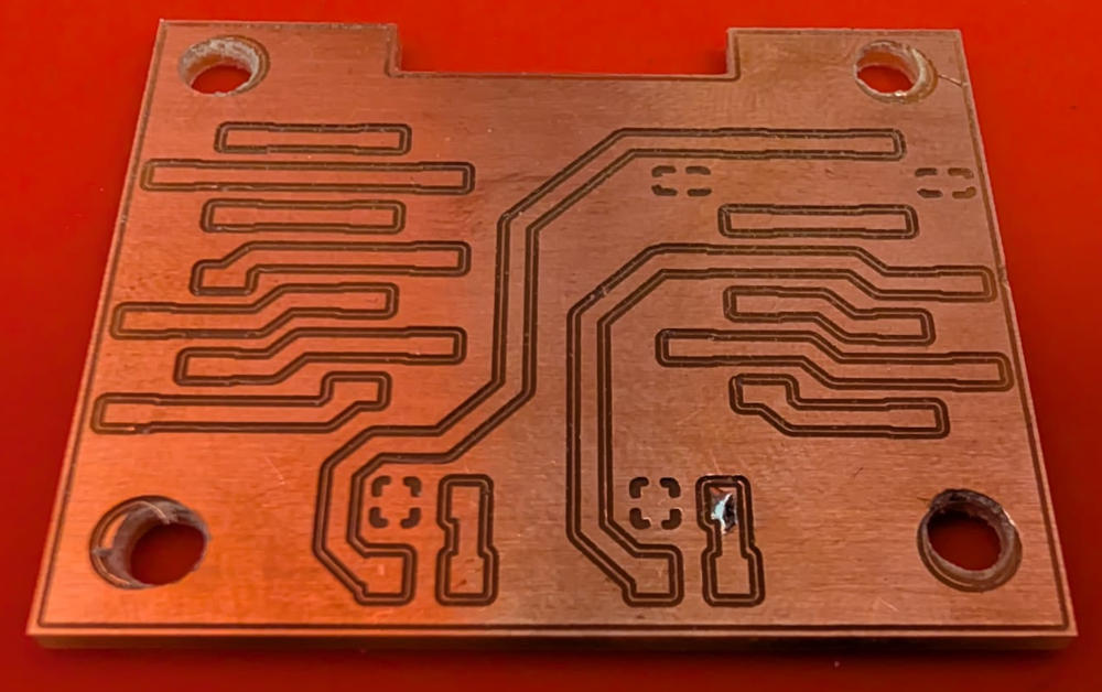
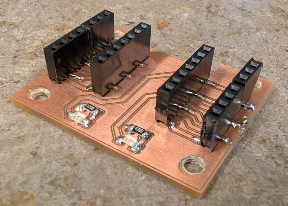
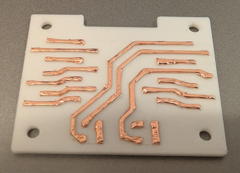
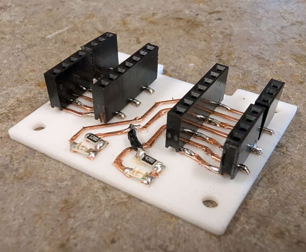
Here's the final result :
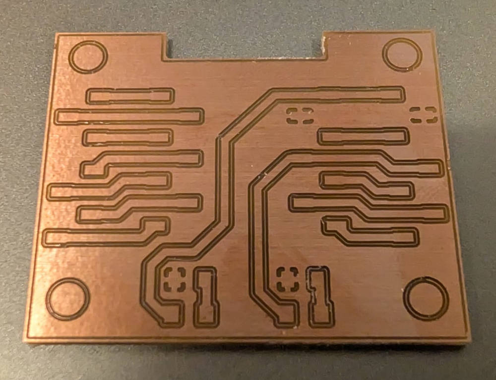
I forgot to make the outer holes with the PCB milling machine so I just did them with a drill driver.
Before soldering the components on my PCB, I do a continuity test with a multimeter to make sure there aren't any short-circuits.
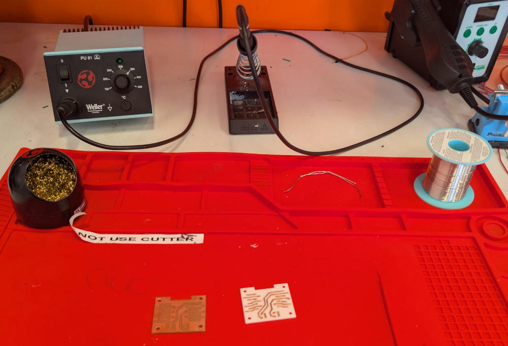
Once everything is checked, I move on to the soldering. Our FabLab has a Weller PU 81 soldering station.
For the placement and soldering of the tiny components, in my case, the resistors and the leds, I first put a bit of solder on the PCB.
Then solder one of the pins of the component.
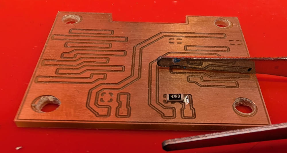
And finally, solder the second pin.
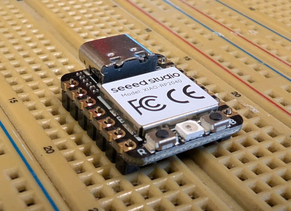
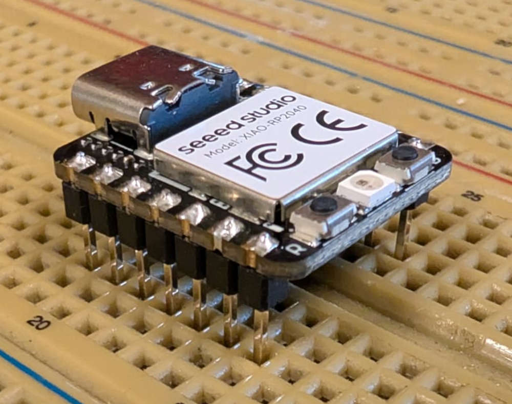
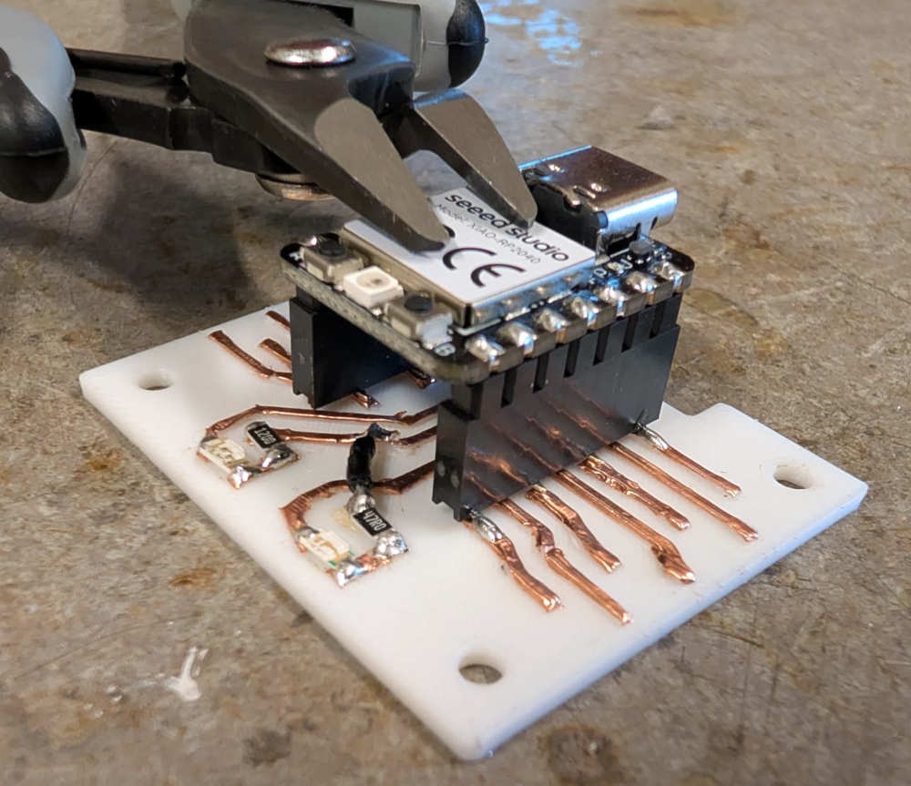
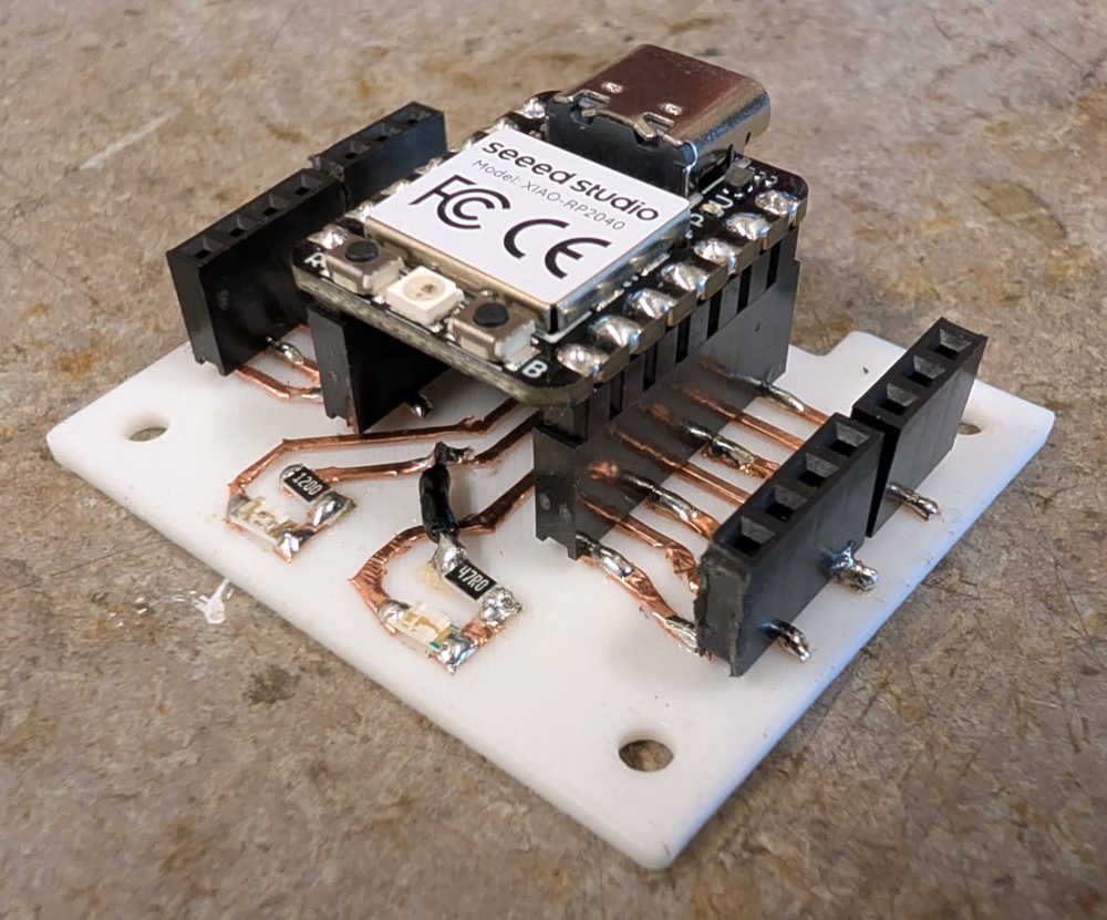
For the female headers, I'll use the microcontroller to align them correctly. To solder the microcontroller's male headers, I use a breadboard.
Once it is well positioned, I solder first the inside female headers.
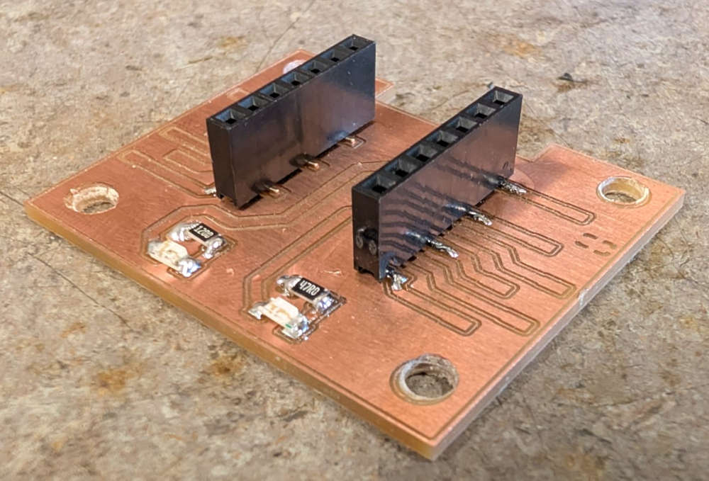
Then, I solder the outside female headers.
I do one last multimeter continuity test to make sure I didn't create any short-circuit.
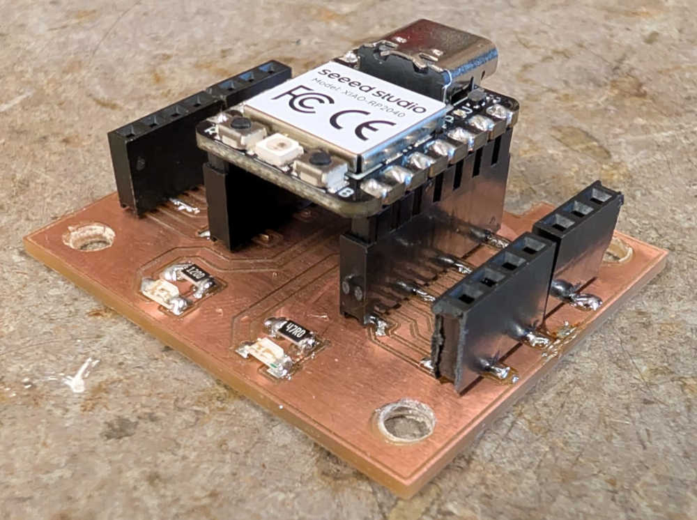
Here's the final result :
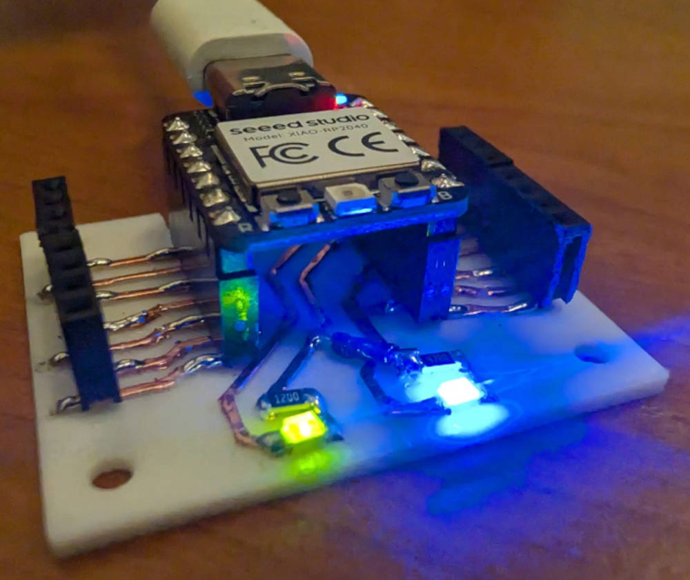
Now for a little test, I do a little code to blink the blue led every 0,5 seconds.
                                            ###########################
                                            ### Code in MicroPython ###
                                            ###########################

                                            import machine	# For hardware functions
                                            import time		# For time functions

                                            led = machine.Pin(3, machine.Pin.OUT)	# Set pin 3 (blue led on the shield) as an output

                                            while True:			# Infinite loop
                                                led.toggle()	# Change the led's status
                                                time.sleep(0.5)	# Delay
Making a PCB with a 3D printer
Like Neil did, our Fab Academy instructor, Patrick, showed us different ways to make PCB, from typical applications to "weird" ones.
One of those was with a 3D printer and copper tape.
The link explains how to do that, I simply followed every step.
First I have to slightly modify my PCB because it won't have a ground plane, so I have to had the ground tracks. One of the track was complicated so I'll just use a wire (blue line).
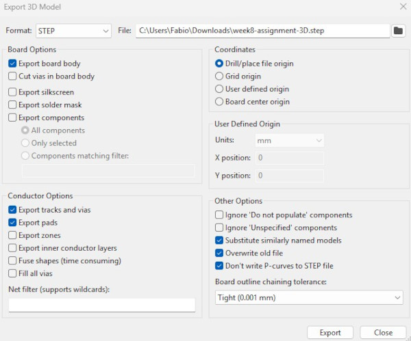
Then, via KiCad, I export the 3D model of my PCB. I need to go to File, then Export and select STEP/GLB/BREP/XAO/PLY/STL....
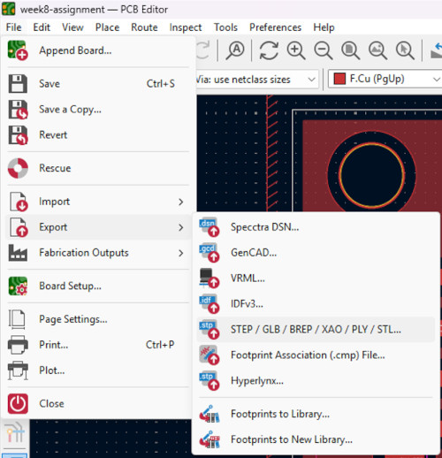
A new window appears, I have to check : Export board body, Export tracks and vias and Export pads (I also had to uncheck Export components).
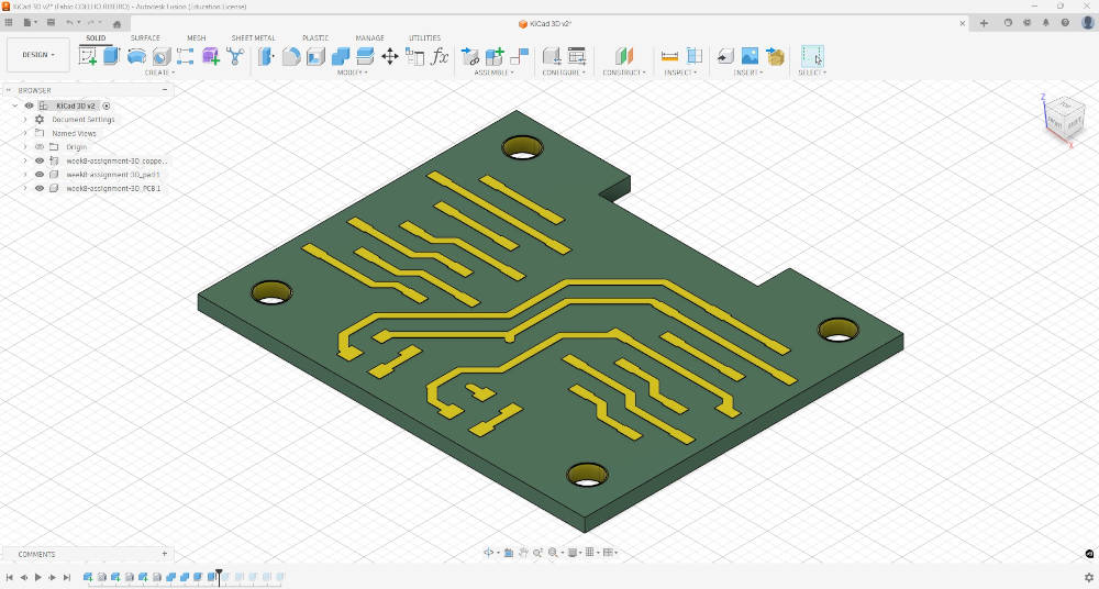
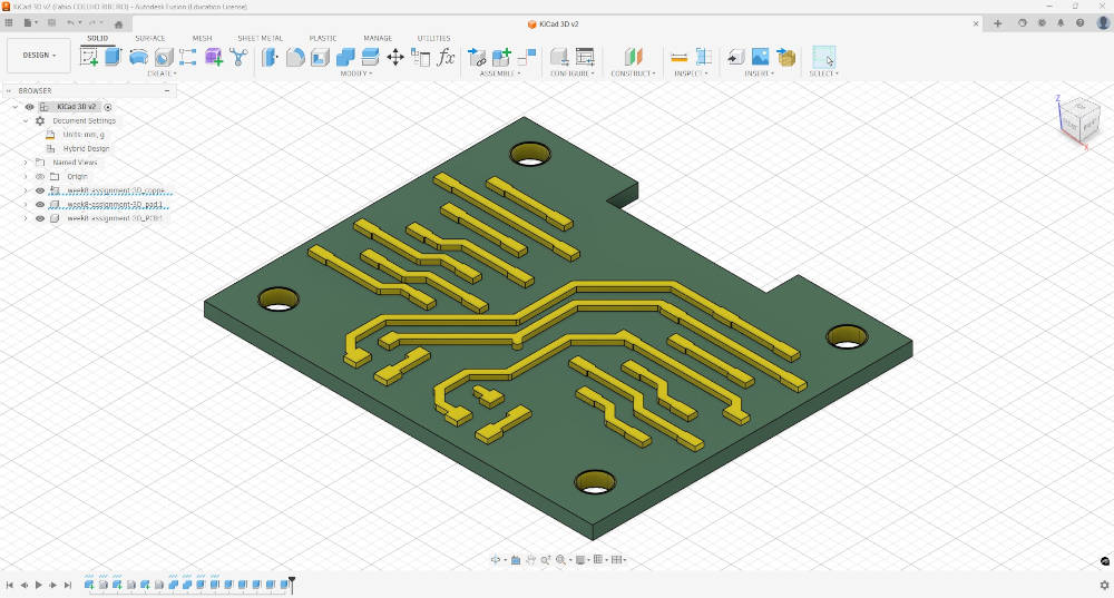
Then, I open, the 3D file in Autodesk Fusion.

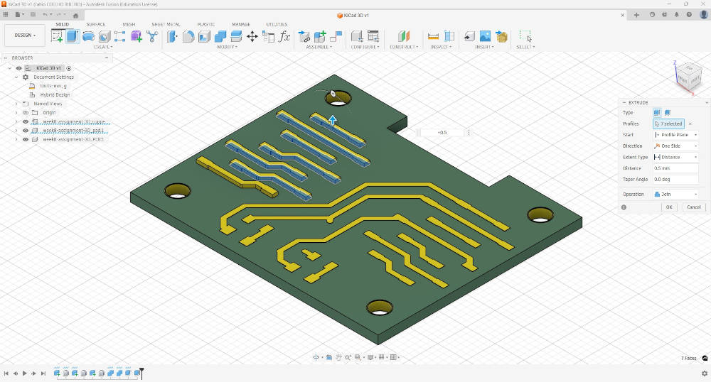
To simplify extruding the tracks and pads, I have to do multiple steps, first I have to combine every tracks and pads together.
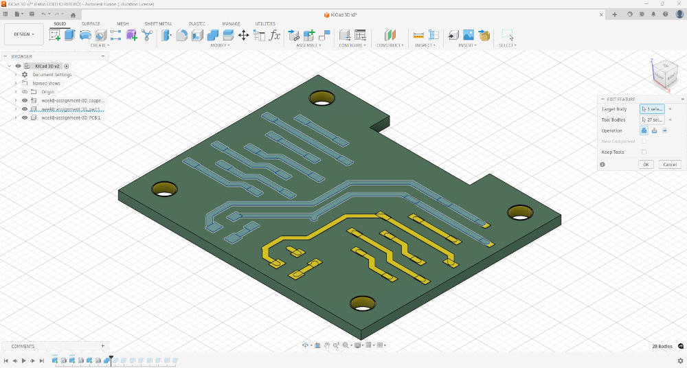
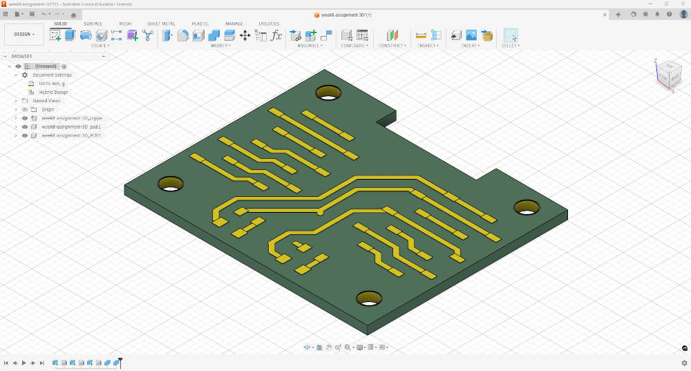
Then I extrude every tracks by +0.005 so all tracks and pads are on the same level.
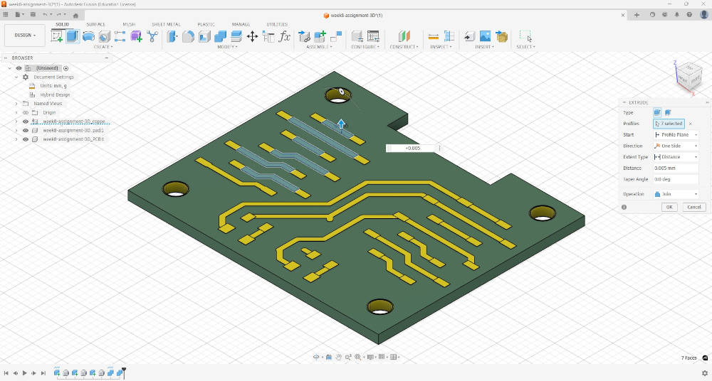
Then I extrude every tracks and pads by +0.5.
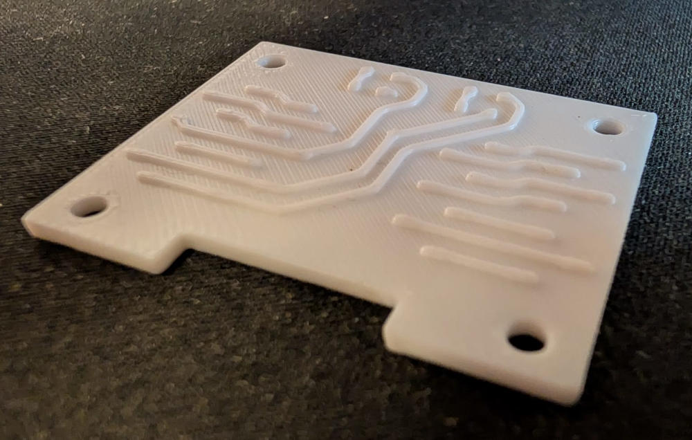
Then, I 3D print the piece.
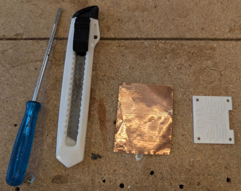
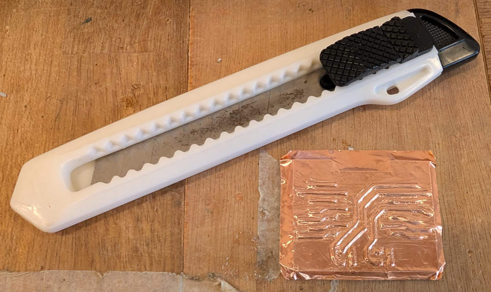
Now for the manual part, I simply have to use a screwdriver, a cutter and some copper tape.
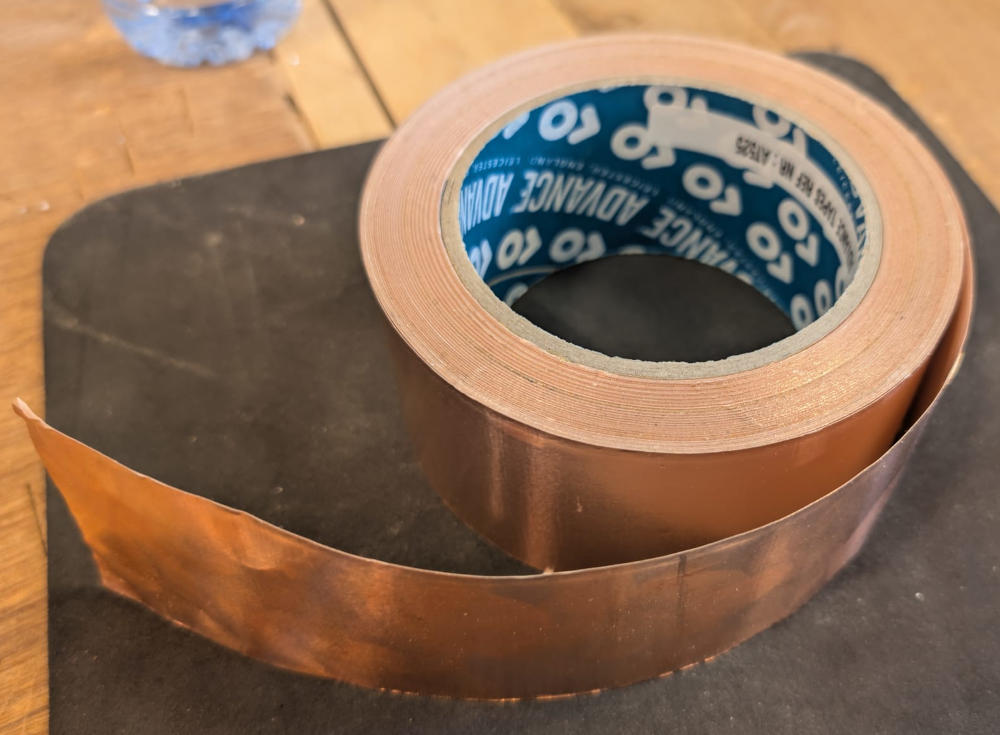
I apply the tape on the 3D printed PCB and use the screwdriver to push the tape down and make sure it sticks and fits.
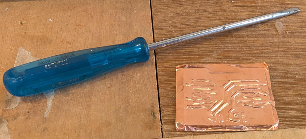
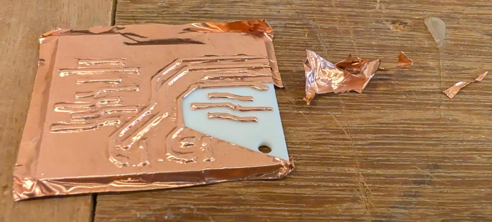
Finally, I use a cutter to remove the excess copper and keep only the copper on the tracks.
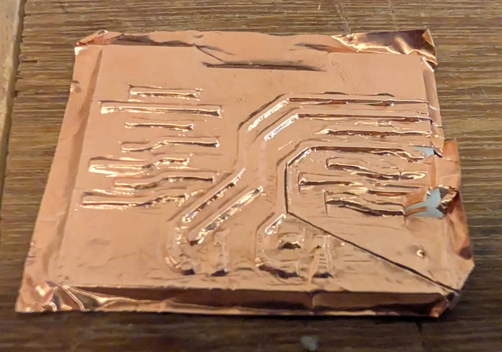
Here's the final result :
Now for the soldering, I do it the same way as the PCB milling machine method, the only exception being the black wire to connect the grounds together.
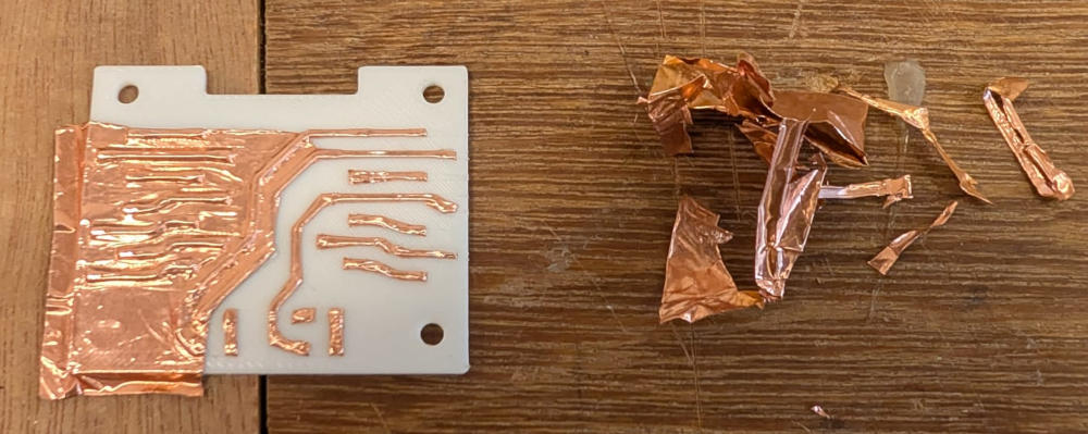
Here's the final result :
I do exactly the same test code on this PCB as well, at first It didn't work because one of the ground tracks was not well connected, but after soldering it to correctly, It worked.
Board house
Now to simulate what It would look like if I had to order the PCB in a board house.
I already have a lot of experience with JLCPCB, a popular board house in China.
To start, I'll need all of the Gerber files of my board, so I open my PCB in KiCad and I export them all.
Then, on JLCPCB, I click Get Instant Quote, a new windows appears to configure our PCB.
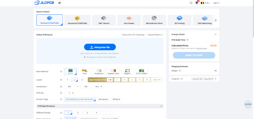
The first thing to do is import the gerber files from a ZIP folder, I have to click Add gerber file and select the folder, the website will process all of the files and give me a first glimpse of the final result. The PCB looks a bit weird because I must have added a special and useless layer.
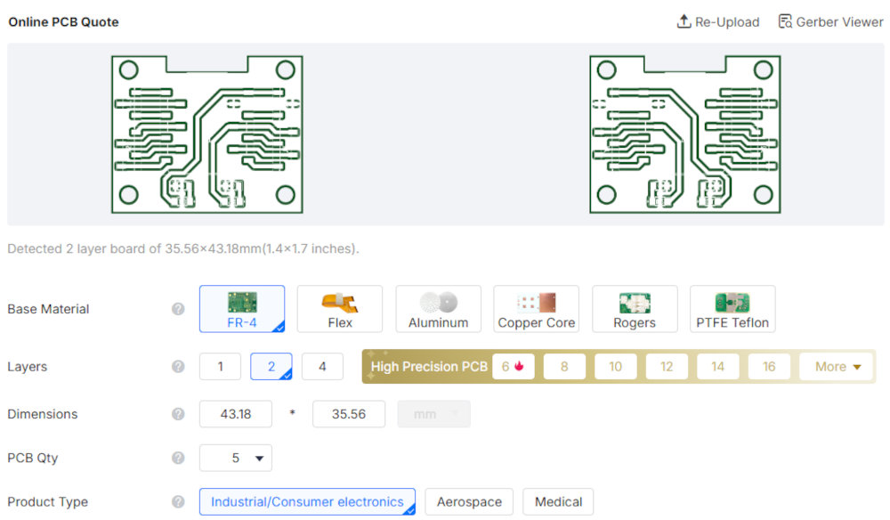
The website can already identify some characteristics like the lengths, the number of layers, ...
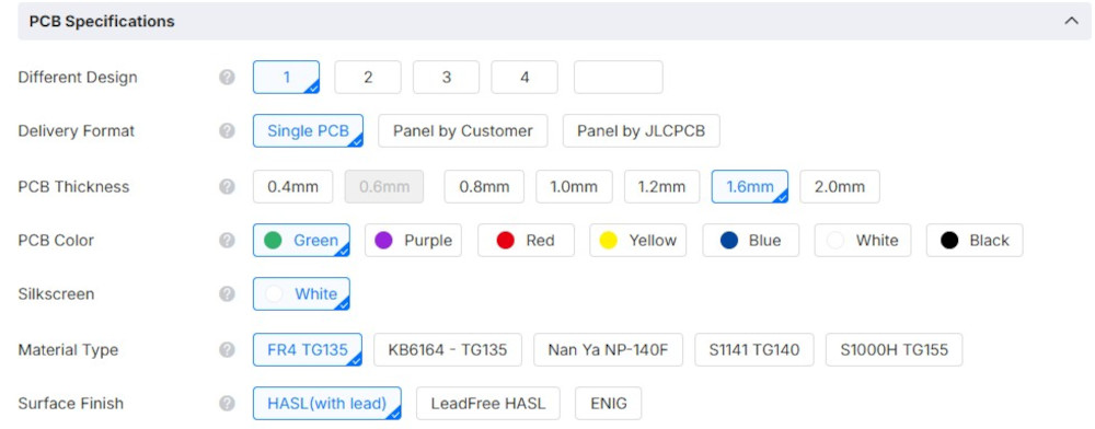
Now I can get creative and choose : the base material (FR-4, flex, ...), the numbers of PCBs to order, the color of my PCB, the outer copper weight and something I usually choose, the assembly, this gives me the option to receive my PCB with the components (if they have it) already soldered on it, this increases the price since you also to buy the components.
When everything is good, I press SAVE TO CART.
Problem(s) met
-
Bantam - Tracks too close
In my first design, some of my tracks were too close to each other and I didn't want to manually fix or cut them myself after the work, so I simply moved them for better spacing in KiCad.
-
Bantam - Broken end mill
I accidentally broke an end mill during my first time, I believe it was because I didn't do an initial machine homing before changing tools.
Useful file(s) (Click to download)
- Shield for XIAO RP2040 - PCB Milling machine (KiCad)
- PCB 3D models (step and f3d) (Autodesk Fusion)
- Shield for XIAO RP2040 - 3D PCB (KiCad)
- SEEED XIAO RP-2040 Led blink (Thonny)
Assignments checklist
- ✅Linked to the group assignment page.
- ✅Documented how you made the toolpath.
- ✅Documented how you made (milled, stuffed, soldered) the board.
- ✅Documented that your board is functional.
- ✅Explained any problems and how you fixed them.
- ✅Uploaded your source code.
- ✅Included a hero shot of your board.