Prior knowledge
|
I have a bachelor in applied electronics, so I know quite a lot about electronics and designing PCBs (Printed Circuit Board). I already created and bought boards for various projects. |
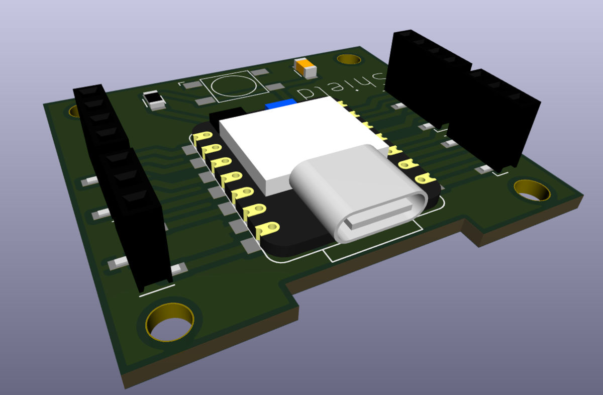
Hero shot
Test equipment
To observe the operations of PCB or a microcontroller, we can use various tools, Jonas Grimaud and Michel Osee explain the tools available at our FabLab.
I worked with Jonas to explain how to use a multimeter and an oscilloscope while Michel worked on explaining how to use a logic analyzer.
Circuit simulation
To simulate a circuit, I am going to use Wokwi and make a simple circuit.
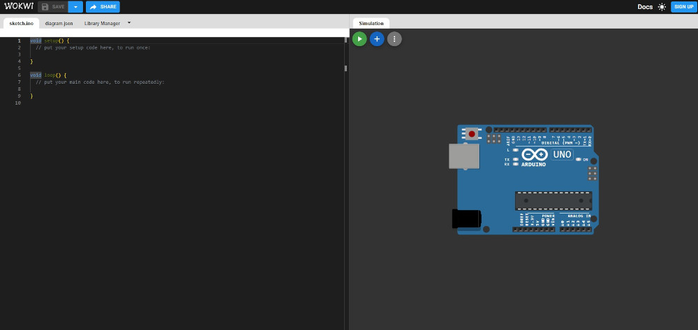
I start a new project from scratch based on an Arduino Uno microcontroller.
After looking what was available, I decide to make a circuit with a joystick, a I2C LCD screen and 4 RGB LEDs, the LEDs are by default lit up in red and when the joystick is pushed to a position, the LED in that position is lit up in green and the screen displays the current position.
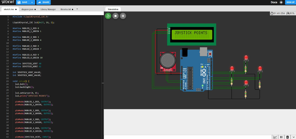
Once the circuit and the code are ready, I press Start the simulation and press the arrow keys on my keyboard to move the joystick.
EDA (Electronic Design Automation)
EDA's are software helpful to create and design PCBs. You usually start by making a schematic diagram and then translate it into a PCB or the other way around. You can also create custom footprints for your components.
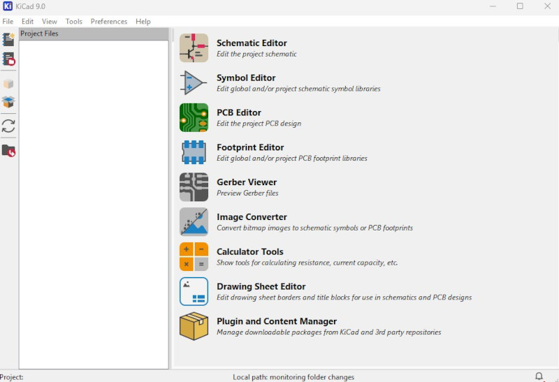
For this week's assignment, I'll try KiCad for the first time, special thanks for Michel who gave us a tutorial on how to use it.
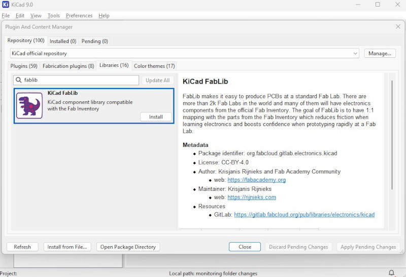
Before starting a diagram, I need to add the library from the Fab Academy for the inventory available at the FabLabs. I need to press Plugin and Content Manager, go to Libraries, type FabLib in the search bar to find KiCad FabLib and then press Install and Apply Pending Changes.
To start designing, I need to create a new project, which creates a new schematic and new PCB.
I'll start with the schematic and then update the PCB when I'm done.
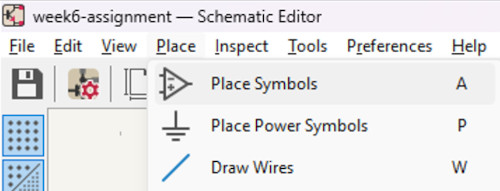
The main tools I'll use are Place Symbols, Place Power Symbols and Draw Wires.
-
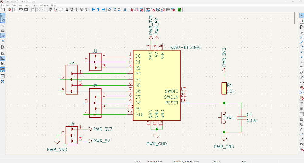
Place Symbols
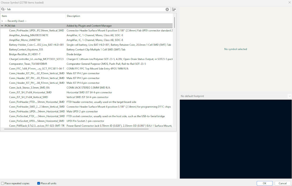
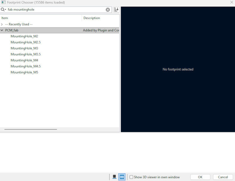
The symbols are basically the components, to access the inventory from the FabLab, I press Place Symbols and type fab in the search bar to access the PCM_fab library. To place a component, I must select one and press OK or double click it.
-
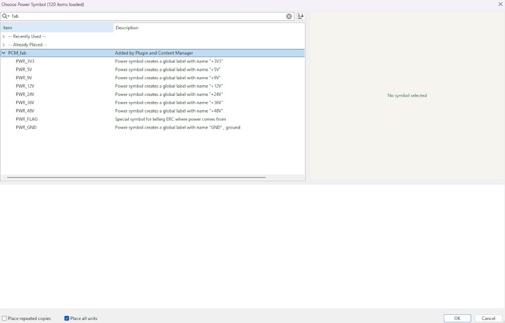
Place Power Symbols
Power symbols are necessary to connect tensions at the right spot or to ease a schematic's drawing. The FabLab's inventory already proposes a few.
-
Draw Wires
The wires are essential on a schematic, they are what connect each components together.
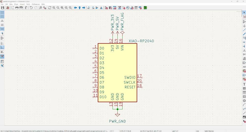
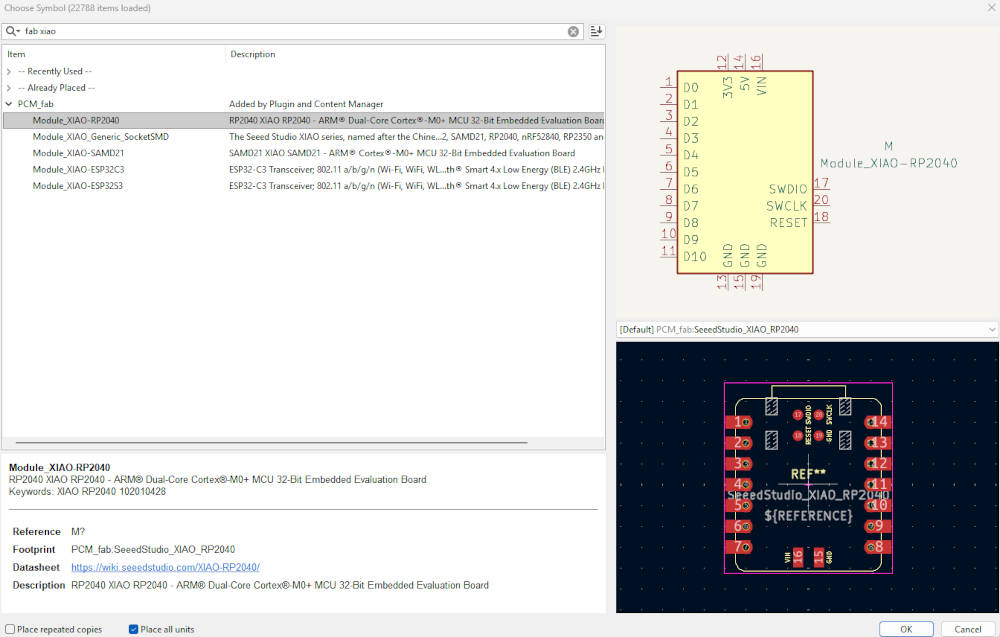
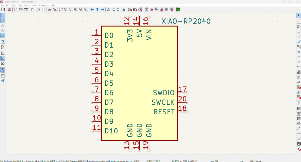
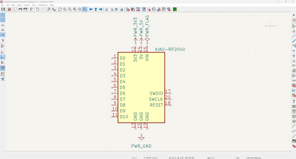
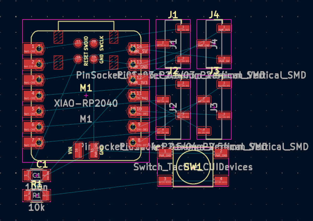
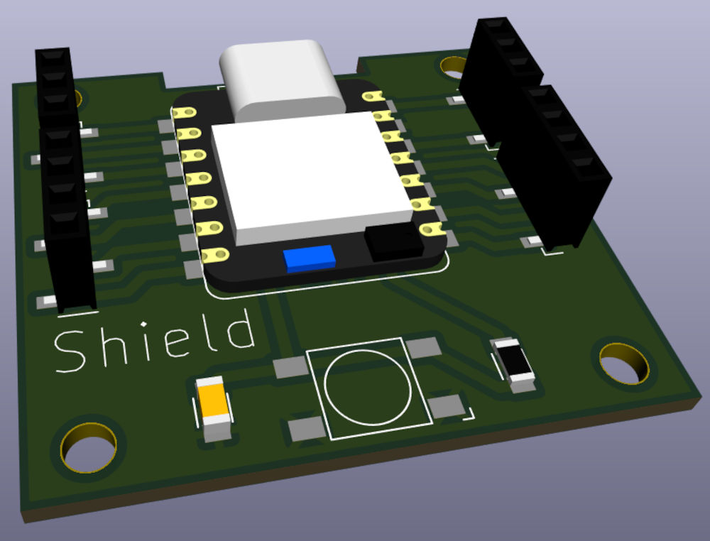
For a simple start, I made a shield for the SEEED XIAO-RP2040, which means I'll be able to easily access its different pins and have a plug-and-play system. I also added another reset button because the one on the microcontroller is really tiny.
-
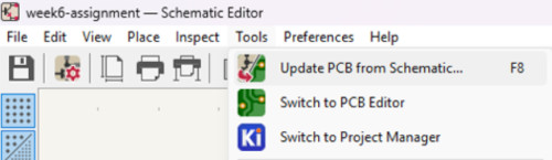
PCB conversion
Once the diagram is finished, I can start working on the PCB. For that, I must press Tools and then Update PCB from Schematic....
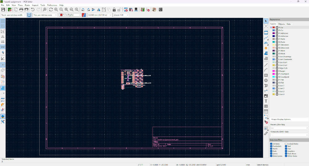
This opens the PCB editor window with a message to confirm the update, I have to press Update PCB to apply the changes.
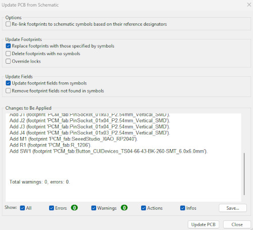
This will place all the components together with no connections.
-
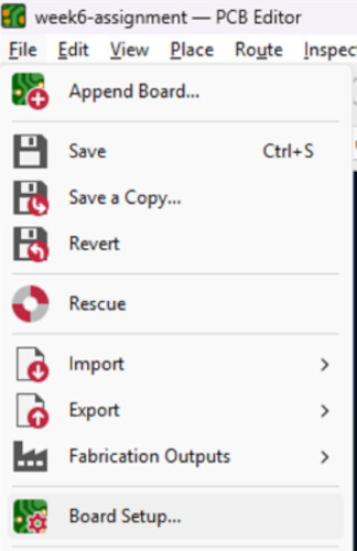
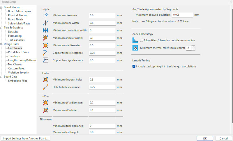
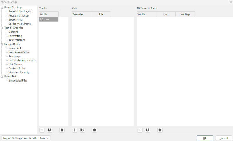
Design rules
To edit the design rules, I have to press File, and then Board Setup..., a new window will pop up. The main parameters I'll modify are in the Constraints and Pre-defined Sizes sections. These parameters may vary between applications or the machines that will make the PCB.
-
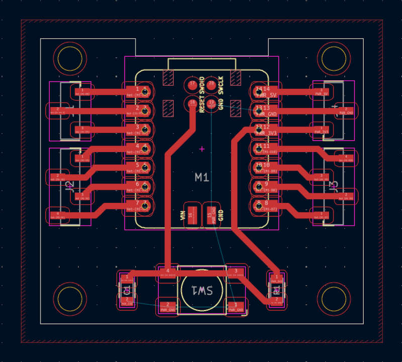
PCB design
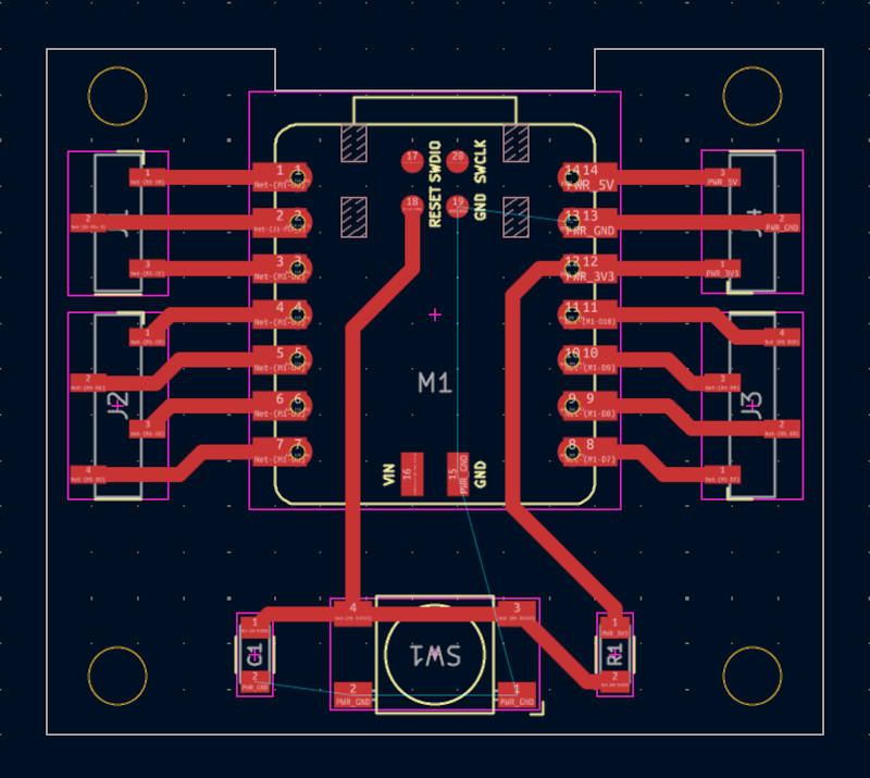
At this point I have to change the position of the components myself and create the tracks by pressing "X".
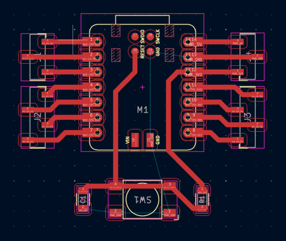
Usually I leave the reference of the components to easily identify it later when soldering but for this example, I'll remove them since there are not a lot of them.
I'll place holes on the shield so it can be screwed and not move. To add them, I simply open the footprints library from the Fab Academy inventory and place them.
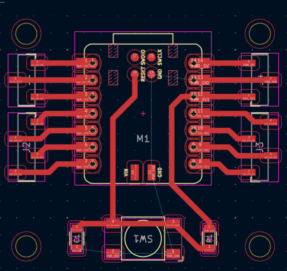
For the board outline, I have to select the Edge.Cuts in the Layers on the right and draw the shape of my board.
-
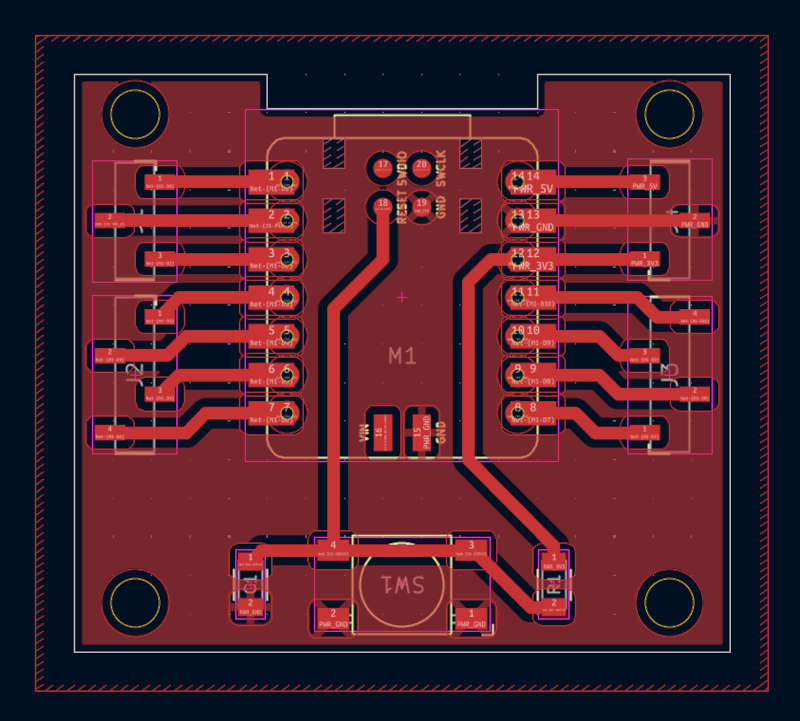
Copper zone
And finally, for the ground pins, I'll connect them all together with a ground plane. I can do that by selecting Draw Filled Zones on the right. A new window will appear asking what power net should be the plane, of course, I choose PWR_GND.
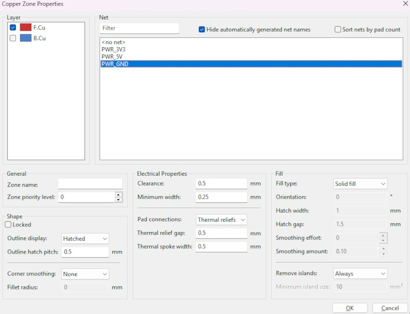
Then I have to draw around the zone I want my ground plane to fill, in this case, everything.
Then by pressing "B", I can fill my board to connect the ground pins together.
I can also add some text, the most important is to choose the good layer which is usually the silkscreen layer and choose either top/face or bottom.
-
Design rules check
Now that my design is finished, I can run a DRC (Design Rule Check) to make sure everything is correct depending on the parameters I set up at the beginning of my PCB design.
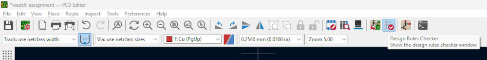
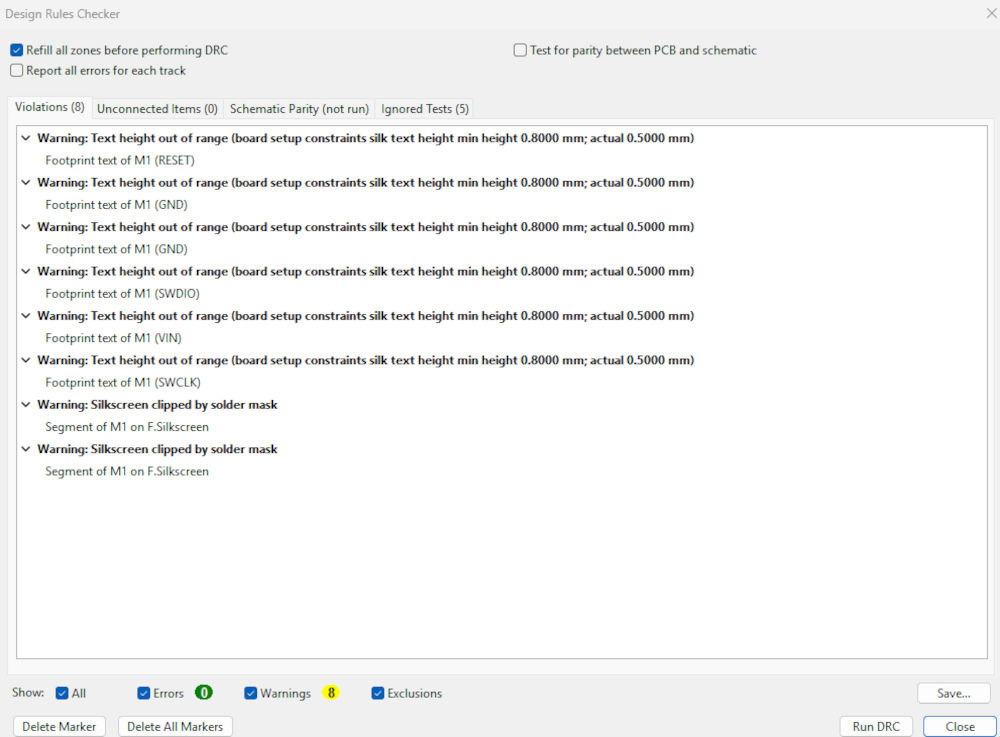
These errors are mainly about the texts or the silkscreen layer but in my case, they don't really matter since I won't add text on my PCB.
-
3D viewer
KiCad also proposes a 3D viewer to see the final result of our PCB.
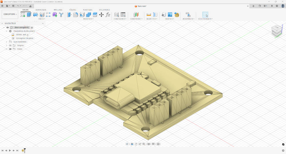
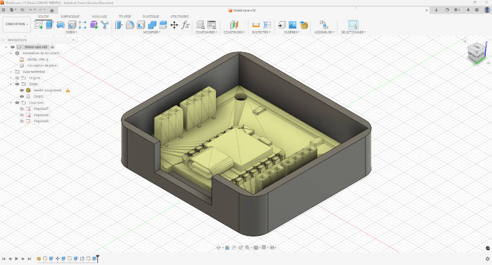
Case design
I am going to create a simple case for my shield using Autodesk Fusion.
Luckily, KiCad give us the opportunity to export our PCB as a STL file via the Export option in the File section of the PCB editor.
I can now import this file on Autodesk Fusion and design a case around it.
Problem(s) met
-
Simulator limits
I tried to add more else if loops for the diagonals of the joystick but it didn't work well, I believe it was because Wokwi doesn't do well with complex operations.
Useful file(s) (Click to download)
- Arduino Uno, joystick, I2C LCD screen and RGB LEDs (Wokwi)
- Shield for SEEED XIAO-RP2040 (KiCad)
- 3D model of the shield (STL)
- 3D model of the case of the shield (Autodesk Fusion)
Assignments checklist
- ✅Linked to the group assignment page.
- ✅Documented what you have learned in electronics design.
- ✅Checked your board can be fabricated.
- ✅Explained problems and how you fixed them.
- ✅Included original design files (Eagle, KiCad, etc.).
- ✅Included a hero shot.