This week we focused on electronics production by physically fabricating a PCB (Printed Circuit Board) using the lab's milling machine. The process went from reviewing a digital design all the way to a soldered and functional board. The general workflow was:
Reviewing and correcting the PCB design from week 6 to make sure it was ready for fabrication.
Exporting the Gerber files from KiCad, which contain the trace and drill information of the board.
Converting the Gerber files to PNG using the FabLab's Gerber2PNG tool.
Loading the PNGs into Mods Project to generate the RML files for the milling machine (a different one for the traces/outline/drill, each with its own tool configuration).
Setting up the Roland SRM-20 machine: loading the correct tool, setting the X, Y and Z origins, and sending the RML files (drills, then traces, and lastly the board outline).
Repeating in case its needed (I did the milling process twice since the first attempt had issues, so I adjusted and re-ran it until I had a clean board).
Soldering the components onto the milled PCB.
Programming the board to verify it works correctly.
To know more about our FabLab's machines check the group assignment:
The board I fabricated is a NeoPixel controller: it uses potentiometers to control the behavior of NeoPixel RGB LEDs, allowing manual adjustment of parameters like color or brightness through analog input. The digital side of the process covered the PCB design review, Gerber export, image conversion and toolpath generation. Here you can explore my process:
PCB Design Review in KiCad
Before fabricating, I reviewed and corrected the PCB design I had made in week 6. Once everything looked good, I exported the necessary files for fabrication.
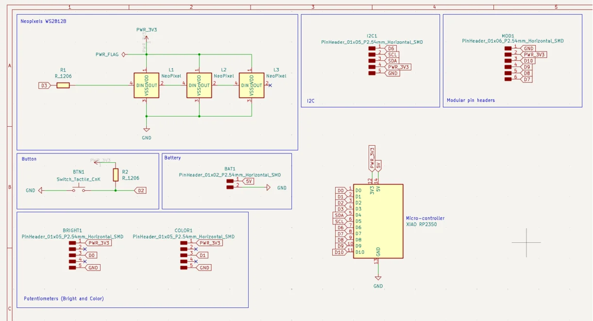
1. Here is my corrected schematic, with all the components and connections properly reviewed.
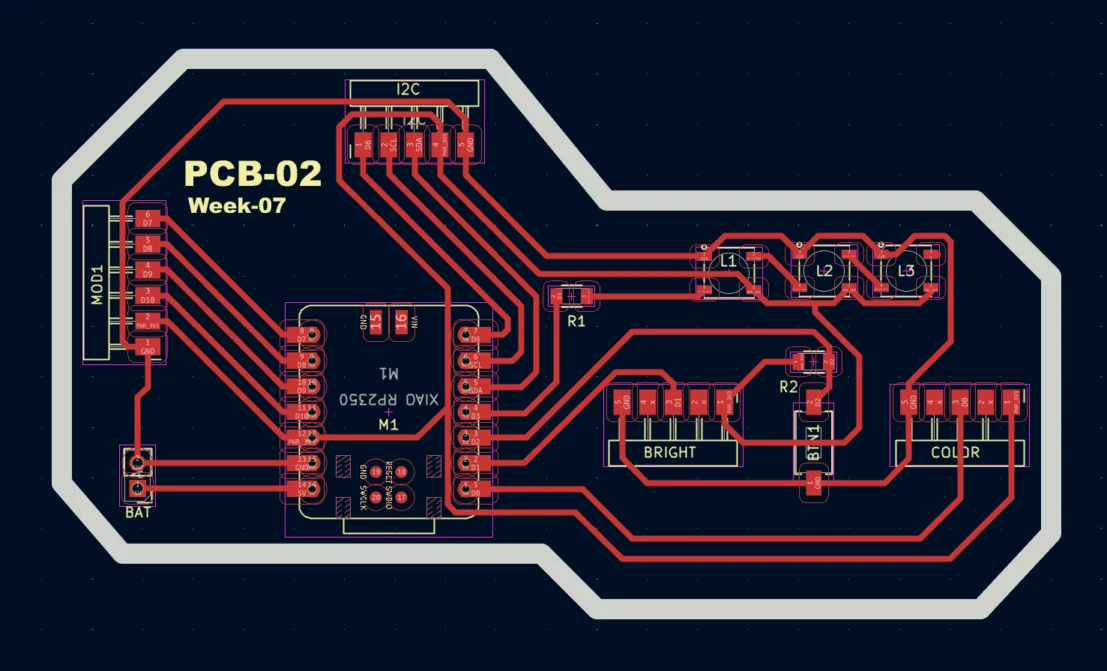
2. And here is the corrected PCB layout, with traces routed and components placed correctly.
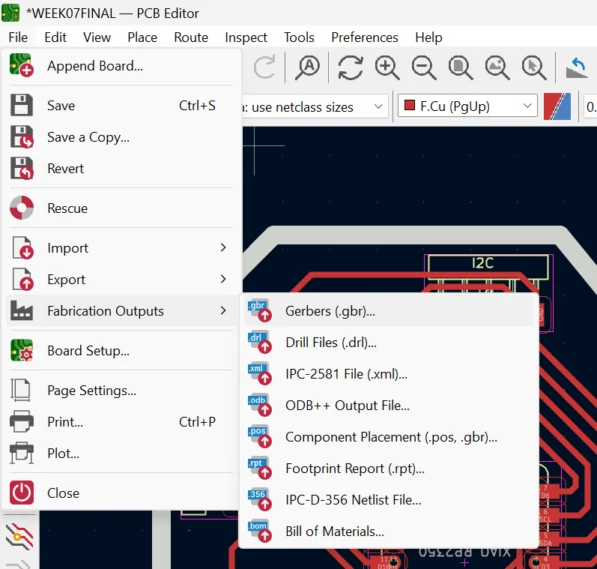
3. To export the Gerber files from KiCad, go to File > Fabrication Outputs > Gerbers. Select the layers you want to export and click Generate.
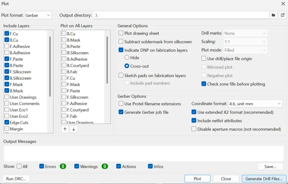
4. A window will appear, select the layers you want to export and click Generate.
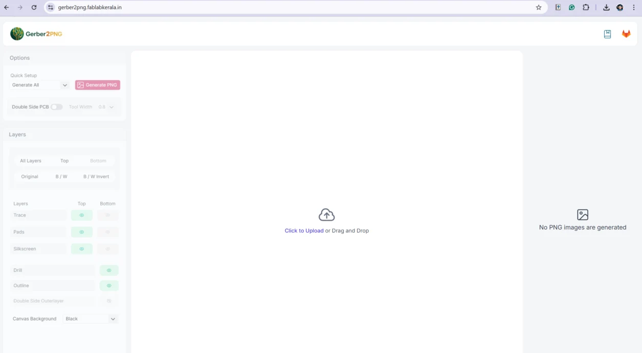
1. This is the default Gerber2PNG page when you first open it.
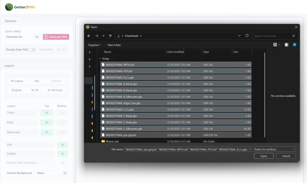
2. Here we select our Gerber files and drill files.
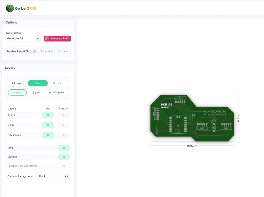
3. The page will process the files and generate a preview of your board.
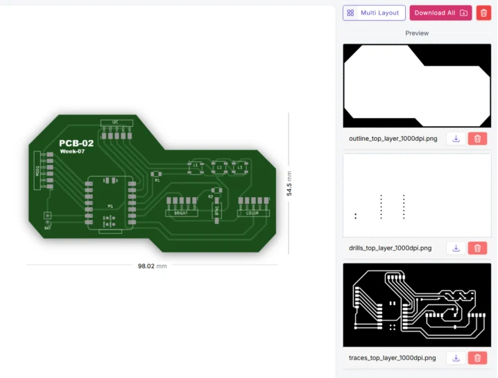
4. Once processed, we can download the resulting PNG images that will be used in the next step (Mods Project).
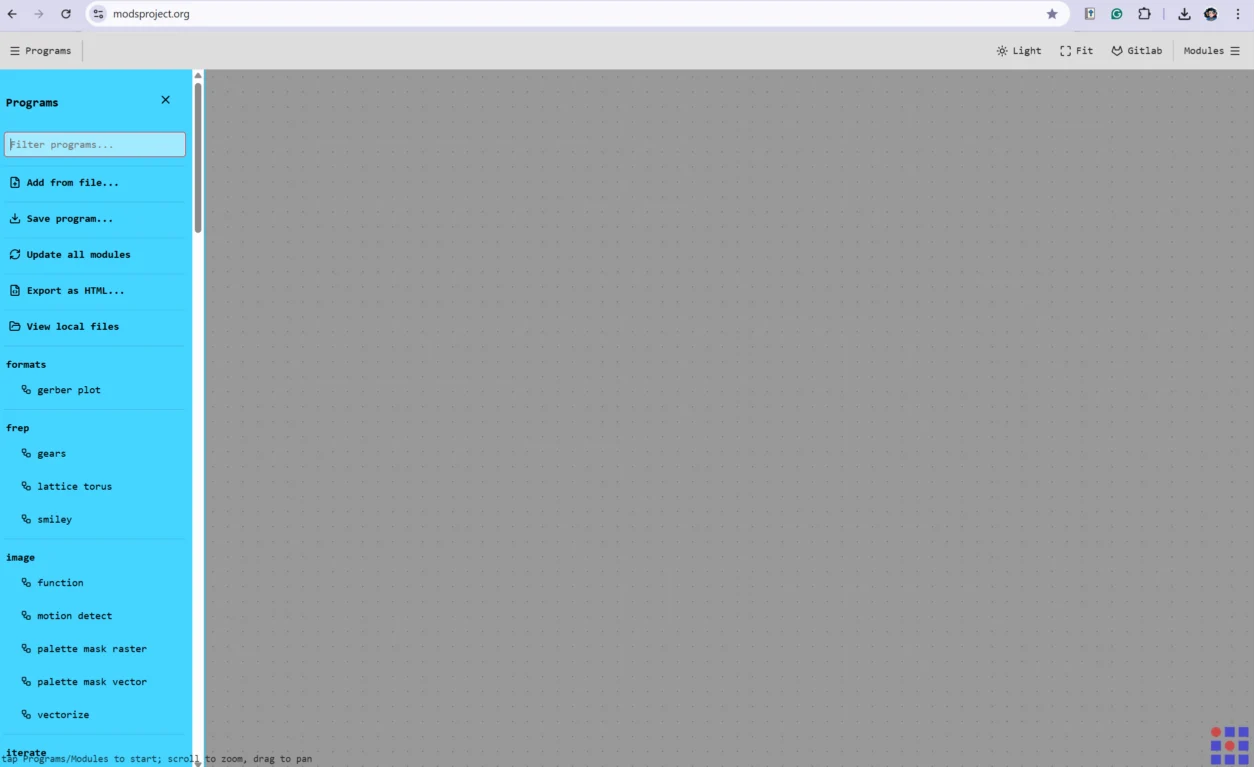
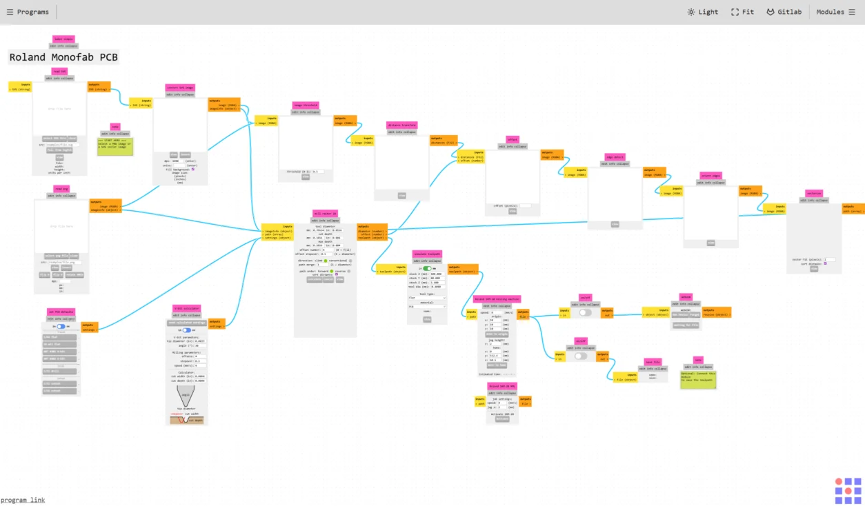
Generating RML files in Mods Project
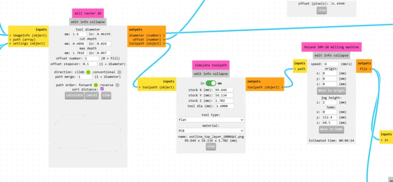
Mods Project converts our PNG images into RML files that the milling machine can read. We generate separate files for the traces, the outline, and the drills (each with its own tool configuration).
1. This is the default Mods Project interface when you open it.
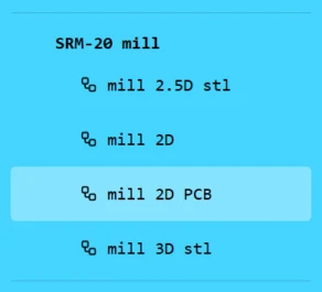
2. We right-click to open the menu and select our machine in this case the Roland Minimill (SRM-20).
3. After selecting the machine, a default node interface will appear.
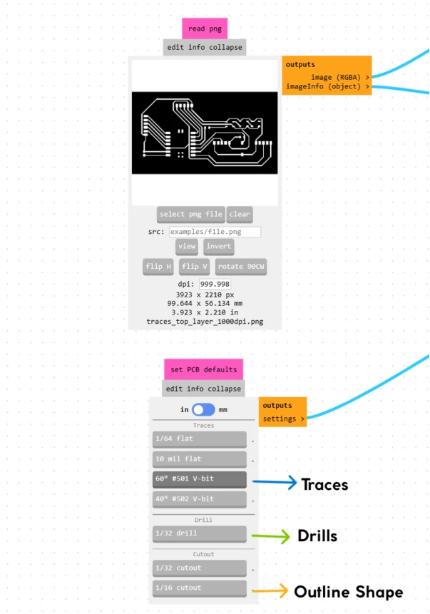
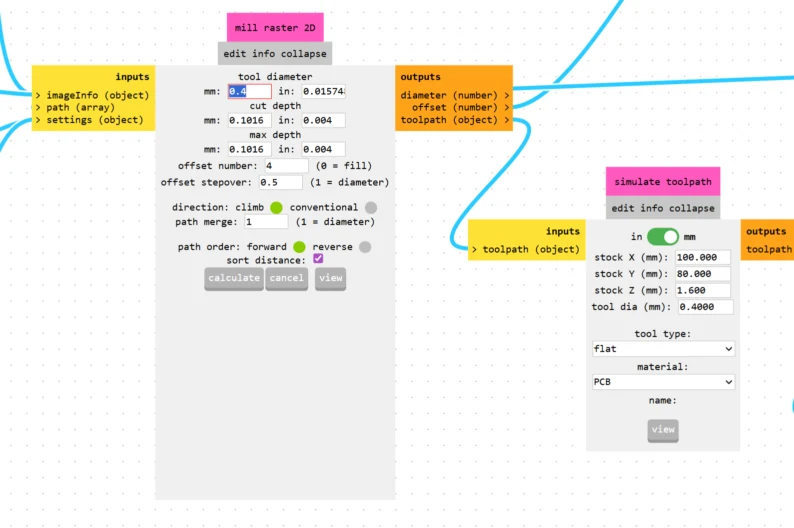
4. Then we load our PNG image into the corresponding input node. And select the tool type depending of the work. For the traces, we use a 60º #501 V-bit engraving tool. For drilling a 1/32 drill and for cutout a 1/16 cutout.
5. Here we modify the tool parameters: diameter to 0.4 mm, a cut depth of 0.1016 mm, and offset overlap of 4 (these for the traces).
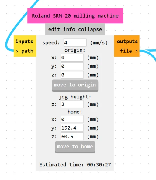
6. We also set the origin position to 0 (X, Y, Z offset) and the cutting speed of 4 mm/s.
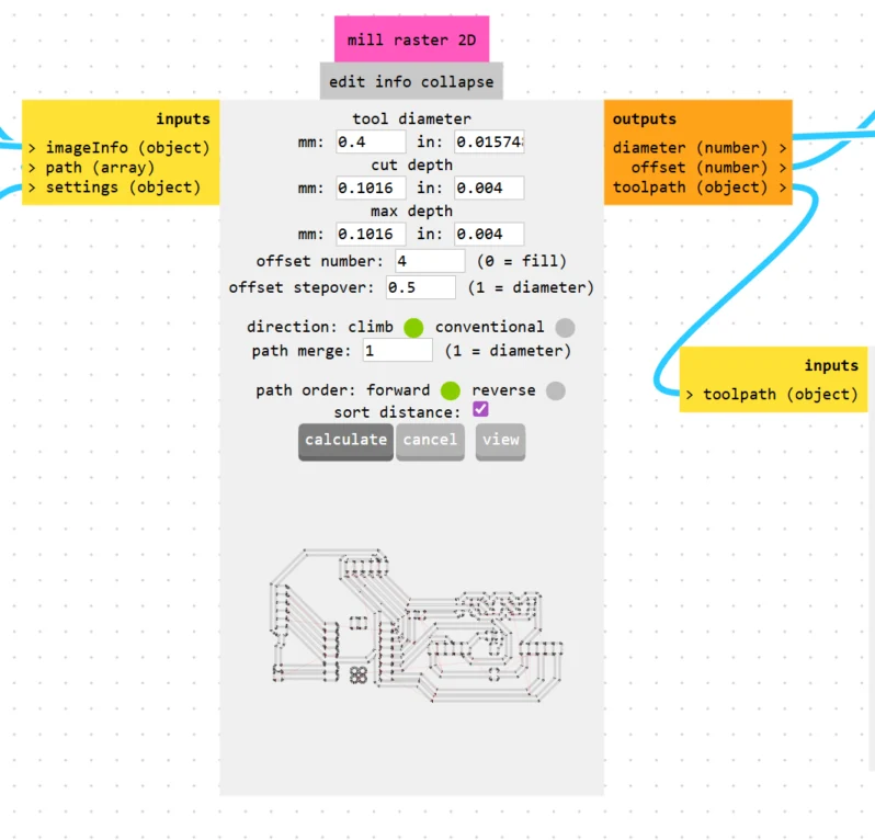
7. Once all parameters are set, we calculate the toolpath.
8. Here is the preview on how it looks. Then download the RML file by activating the "Edit info collapse node".
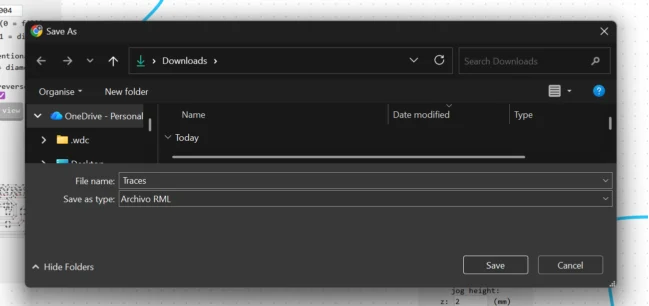
9. Then we download and rename our RML file.
And we repeat the process for each operation, changing the tool and parameters as needed. For example for the cut out we set the tool diameter to 1.6 mm, a cut depth of 0.6096 mm, and a max depth of 1.7018 mm. Lastly we can maintain the 4 mm/s speed.
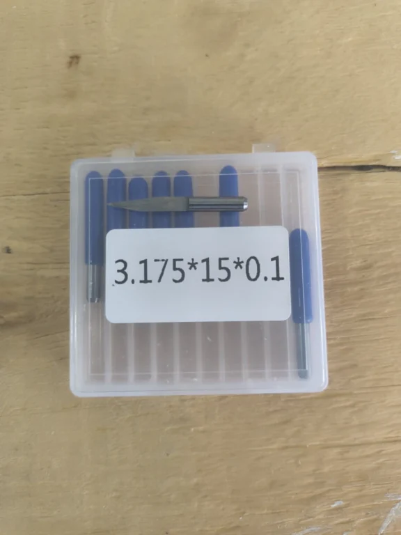
This is the V-bit tool used for the traces.
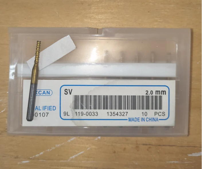
And this is the 1/16 cutout tool for the outline.
Physical Process
With all the digital files ready, the next step was to actually cut, solder and program the board. This part of the process is more hands-on and requires careful machine setup, patience during soldering, and troubleshooting when things don't go as planned.
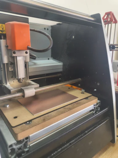
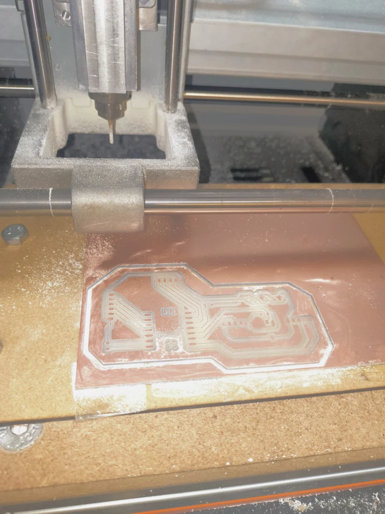
Cutting the PCB on the Roland Minimill
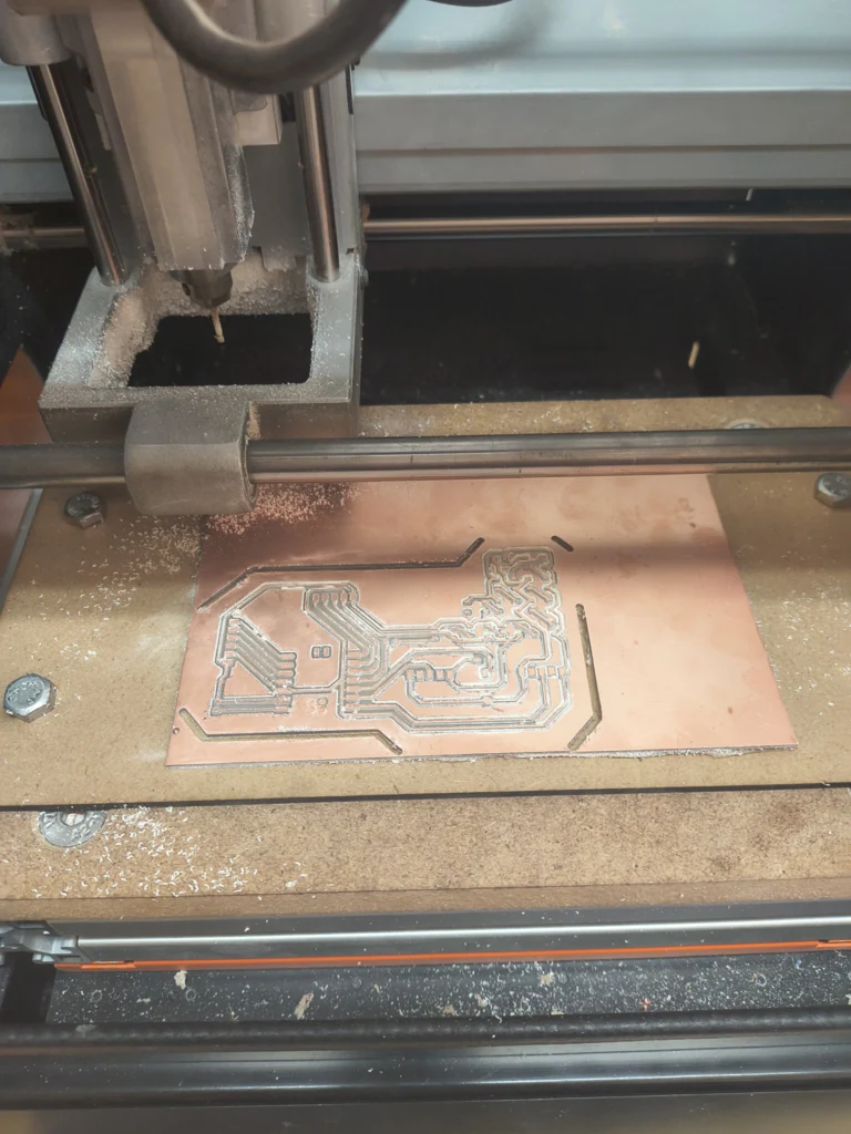
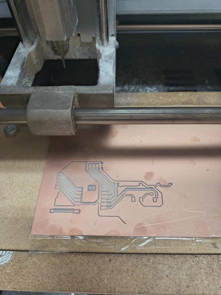
With our RML files ready, we proceed to physically mill the board. The order of operations is: traces first, then drills, and finally the board outline.
1. We attach our copper board to the sacrificial bed using double-sided tape, making sure it is flat and well secured.
2. Then we secure the sacrificial bed to the machine table using the fixing screws/nuts so nothing moves during the cut.
3. We install the V-bit tool for the traces (this tool is for traces, for drills and cutout we need another one).
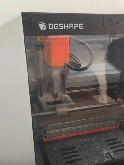
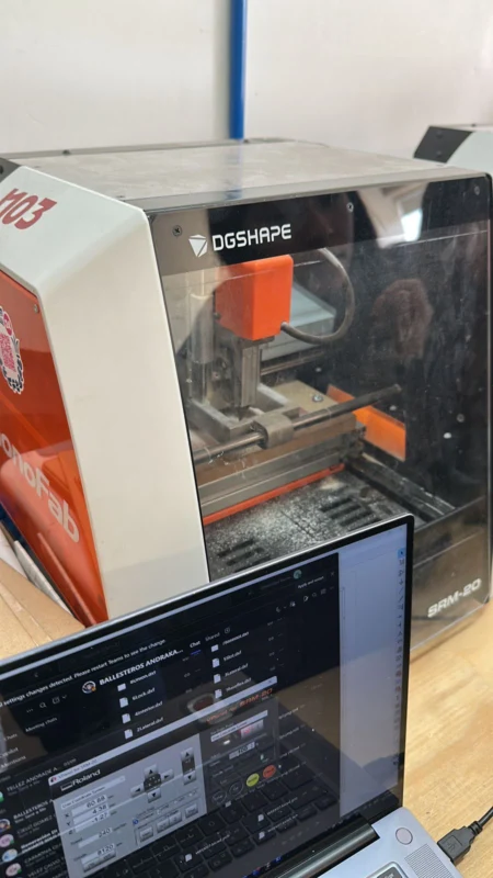
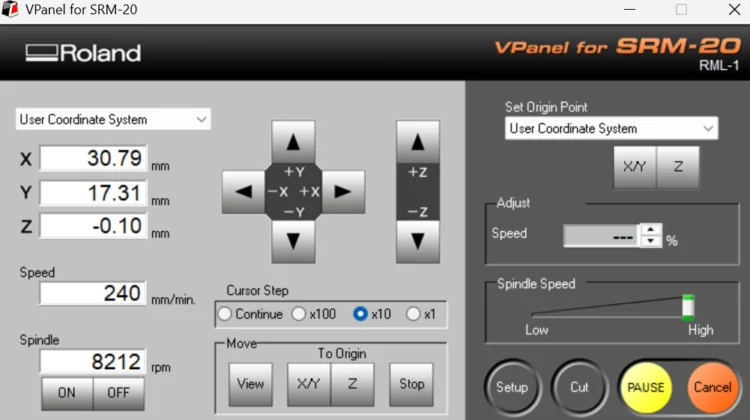
4. We turn on the machine and open VPanel on the computer, making sure the USB cable is connected.
5. We set the X and Y origins by moving the tool to the desired starting corner of the board.
6. Then we set the Z origin with the tool spinning, carefully lowering it until it just touches the copper surface and setting that as Z zero.
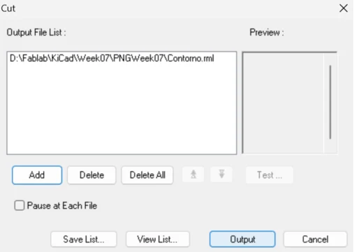
7. After configuring the origins, we go to Cut in VPanel.
8. Then we select our RML file (traces first), click Output.
This way the machine will run the cutting process automatically.
Lastly we repeat the process for the cutout traces.
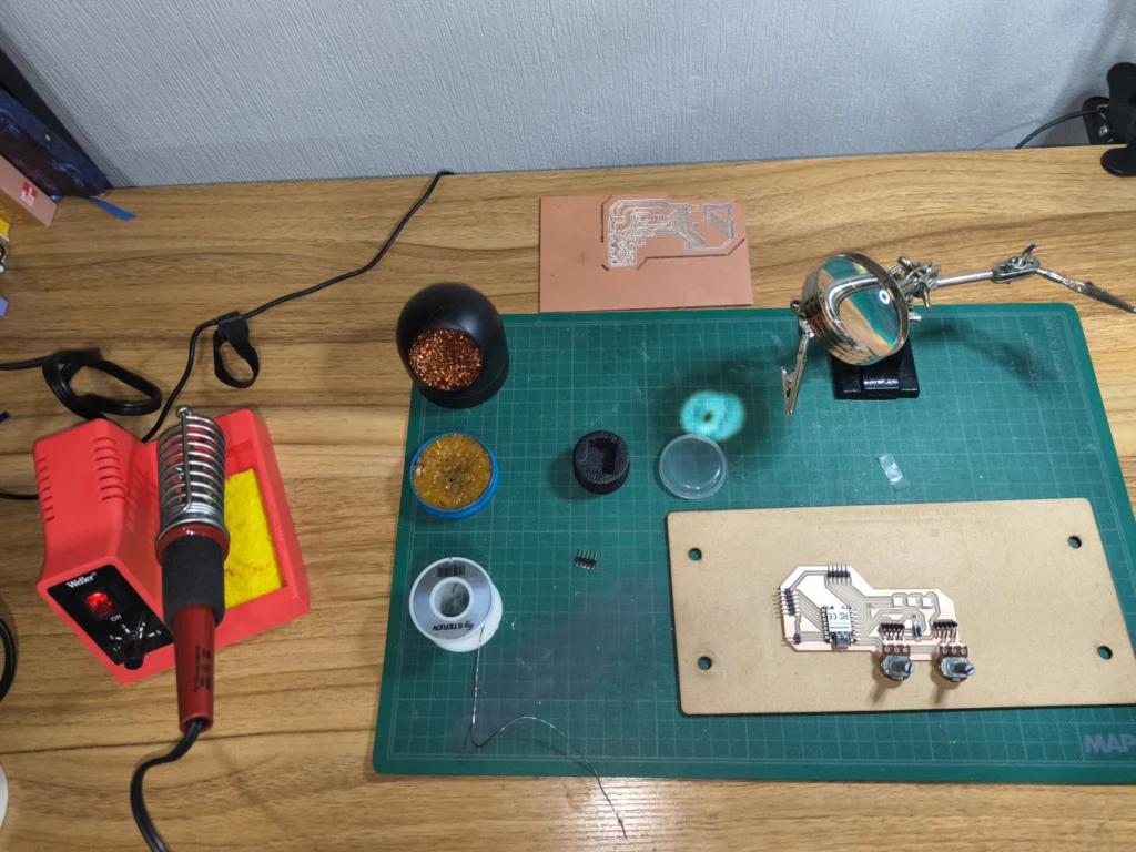
Soldering the components
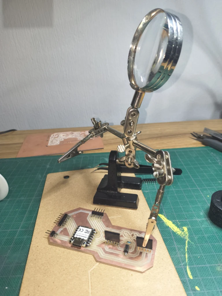
Once the board was milled, I soldered all the components onto it. The process requires patience and precision, especially with small SMD components.
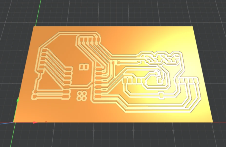
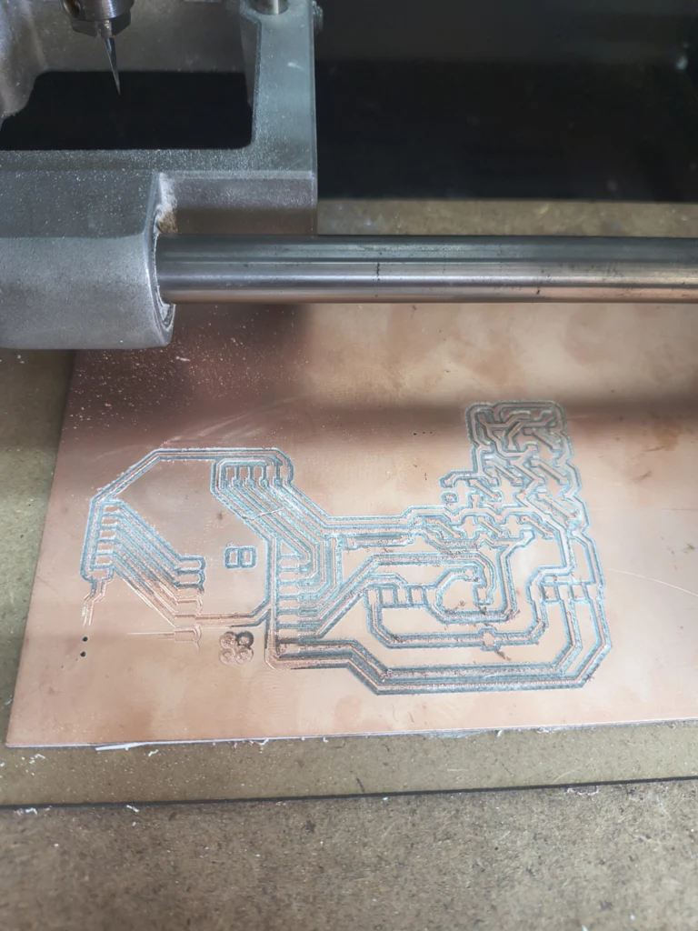
1. Here is how the milled PCB looked before soldering with clean copper traces ready for components.
2. Before starting I ensured I had all the necessary tools and materials ready. Including a soldering iron, flux, solder, brass sponge or damp sponge.
3. Then I prepared the board with all components placed before soldering to ensure proper alignment, and do a component check.
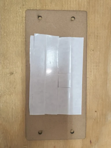
4. I also added insulation tape to protect the board and prevent short circuits.
5. Here is a video of the soldering process.
6. I also used a soldering stand with clamp magnifying tool for pieces that require more precision. However I didn't find the magnify glass comfortable to use.
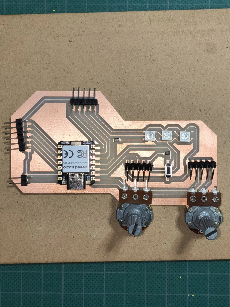
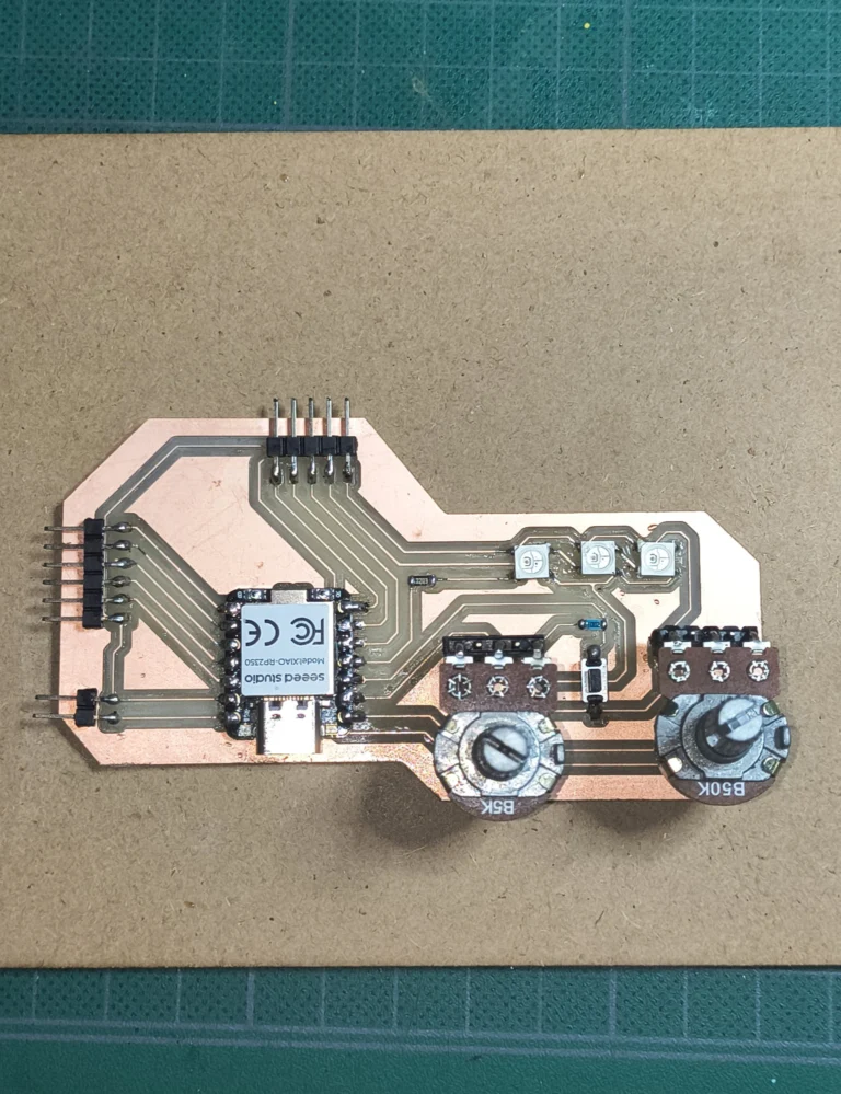
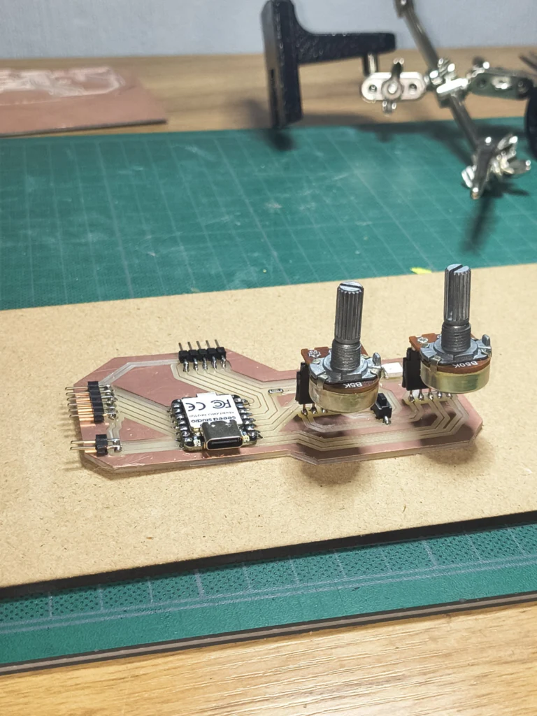
This was the final result of the soldered board (front view).
6. Final result (another angle showing all the components soldered).
Programming the board
To program the board, I used Arduino IDE. The general process involved writing the code, uploading it to the board, and testing its functionality.
Here is a video of the final results, were the left potentiometer controls the RGB color while the right one controls the brightness. When the button is pressed, the LED changes lighting mode
Here is the code I used to program the board. It reads the potentiometer values and button state, and controls the NeoPixel LEDs accordingly.
// ============================================================
//  NeoPixel Controller — XIAO RP2350
//  3x NeoPixels | 2x Potenciómetros | 1x Botón CMK SMD
// ============================================================
//  PINES verificados contra esquemático WEEK07FINAL.kicad_sch:
//    D3  → Datos NeoPixels (via R1 1206)
//    D1  → Pot. B5K  (COLOR1)  → tono HSV
//    D0  → Pot. B50K (BRIGHT1) → brillo
//    D2  → Botón CnK SMD (BTN1, pull-up externo R2)
// ============================================================

#include

// ── Configuración de hardware ────────────────────────────────
#define PIN_NEO       D3   // Pin de datos NeoPixels (via R1 1206)
#define NUM_LEDS      1    // L1, L2, L3 en cadena

#define PIN_POT_COLOR D1   // Pot. B5K  (COLOR1)  → tono HSV
#define PIN_POT_BRILL D0   // Pot. B50K (BRIGHT1) → brillo

#define PIN_BTN       D2   // Botón CnK SMD (BTN1, pull-up externo R2)

// ── Configuración de modos ───────────────────────────────────
#define NUM_MODOS     4    // Total de modos (0-3)

// ── Tiempos ──────────────────────────────────────────────────
#define DEBOUNCE_MS    50  // Tiempo antirebote del botón (ms)
#define SEQ_DELAY_MS  200  // Velocidad de la secuencia (ms)
#define BLINK_DELAY_MS 400 // Velocidad del parpadeo (ms)

// ── Objeto NeoPixel ──────────────────────────────────────────
Adafruit_NeoPixel strip(NUM_LEDS, PIN_NEO, NEO_GRB + NEO_KHZ800);

// ── Variables de estado ──────────────────────────────────────
uint8_t modoActual      = 0;
bool    estadoBtn       = HIGH;
bool    estadoBtnPrev   = HIGH;
unsigned long tiempoDebounce = 0;

unsigned long tiempoAnterior = 0;
uint8_t       ledSecuencia   = 0;
bool          estadoBlink    = false;

// ── Leer potenciómetros ──────────────────────────────────────
uint16_t leerColor() {
  uint32_t raw = analogRead(PIN_POT_COLOR);
  return (uint16_t)((raw * 65535UL) / 4095);
}

uint8_t leerBrillo() {
  uint32_t raw = analogRead(PIN_POT_BRILL);
  return (uint8_t)(10 + (raw * 245UL) / 4095);
}

// ── Detectar click con debounce ──────────────────────────────
bool detectarClick() {
  bool lectura = digitalRead(PIN_BTN);

  if (lectura != estadoBtnPrev) {
    tiempoDebounce = millis();
  }
  estadoBtnPrev = lectura;

  if ((millis() - tiempoDebounce) >= DEBOUNCE_MS) {
    if (lectura != estadoBtn) {
      estadoBtn = lectura;
      if (estadoBtn == LOW) {
        return true;
      }
    }
  }
  return false;
}

// ── Apagar todos ─────────────────────────────────────────────
void apagarTodo() {
  strip.clear();
  strip.show();
}

// ── Modo 1: Todos encendidos ──────────────────────────────────
void modoTodos(uint16_t hue, uint8_t brillo) {
  uint32_t color = strip.ColorHSV(hue, 255, brillo);
  color = strip.gamma32(color);
  for (int i = 0; i < NUM_LEDS; i++) {
    strip.setPixelColor(i, color);
  }
  strip.show();
}

// ── Modo 2: Secuencia ─────────────────────────────────────────
void modoSecuencia(uint16_t hue, uint8_t brillo) {
  if (millis() - tiempoAnterior >= SEQ_DELAY_MS) {
    tiempoAnterior = millis();
    strip.clear();
    uint32_t color = strip.ColorHSV(hue, 255, brillo);
    color = strip.gamma32(color);
    strip.setPixelColor(ledSecuencia, color);
    strip.show();
    ledSecuencia = (ledSecuencia + 1) % NUM_LEDS;
  }
}

// ── Modo 3: Parpadeo ──────────────────────────────────────────
void modoParpadeo(uint16_t hue, uint8_t brillo) {
  if (millis() - tiempoAnterior >= BLINK_DELAY_MS) {
    tiempoAnterior = millis();
    estadoBlink = !estadoBlink;
    if (estadoBlink) {
      uint32_t color = strip.ColorHSV(hue, 255, brillo);
      color = strip.gamma32(color);
      for (int i = 0; i < NUM_LEDS; i++) {
        strip.setPixelColor(i, color);
      }
    } else {
      strip.clear();
    }
    strip.show();
  }
}

// ── Setup ─────────────────────────────────────────────────────
void setup() {
  Serial.begin(115200);
  delay(1000);
  Serial.println("=== NeoPixel Controller iniciado ===");

  analogReadResolution(12);

  strip.begin();
  strip.clear();
  strip.show();

  // Pull-up externo R2 en esquemático → INPUT sin pull-up interno
  pinMode(PIN_BTN, INPUT);
  pinMode(PIN_POT_COLOR, INPUT);
  pinMode(PIN_POT_BRILL, INPUT);

  Serial.println("Setup completo. Presiona el boton...");
}

// ── Loop ──────────────────────────────────────────────────────
void loop() {
  // Debug — abre Serial Monitor a 115200 para ver valores
  Serial.print("BTN: ");
  Serial.print(digitalRead(PIN_BTN));
  Serial.print(" | COLOR: ");
  Serial.print(analogRead(PIN_POT_COLOR));
  Serial.print(" | BRILL: ");
  Serial.println(analogRead(PIN_POT_BRILL));

  if (detectarClick()) {
    modoActual = (modoActual + 1) % NUM_MODOS;
    ledSecuencia   = 0;
    estadoBlink    = false;
    tiempoAnterior = 0;
    Serial.print(">>> MODO CAMBIADO A: ");
    Serial.println(modoActual);
    if (modoActual == 0) apagarTodo();
  }

  uint16_t hue    = leerColor();
  uint8_t  brillo = leerBrillo();

  switch (modoActual) {
    case 0: break;
    case 1: modoTodos(hue, brillo);     break;
    case 2: modoSecuencia(hue, brillo); break;
    case 3: modoParpadeo(hue, brillo);  break;
  }

  delay(100);
}

What does this code do?
It's a NeoPixel LED controller for a XIAO RP2350 board. It lets you switch between 4 lighting modes using a button, and adjust color and brightness with two potentiometers.

Hardware involved
PinComponentFunctionD33x NeoPixelsLED data outputD1B5K PotentiometerControls color hue (HSV)D0B50K PotentiometerControls brightnessD2SMD ButtonSwitches mode

The 4 modes (cycled through with the button)

Mode 0 — Off: all LEDs turned off
Mode 1 — All on: all 3 LEDs lit with the color and brightness from the potentiometers
Mode 2 — Sequence: LEDs turn on one by one in a loop (every 200 ms)
Mode 3 — Blink: all LEDs blink together (every 400 ms)
Code explanation
It's a NeoPixel LED controller for a XIAO RP2350 board. It lets you switch between 4 lighting modes using a button, and adjust color and brightness with two potentiometers.
Hardware involved
PinComponentFunctionD33x NeoPixelsLED data outputD1B5K PotentiometerControls color hue (HSV)D0B50K PotentiometerControls brightnessD2SMD ButtonSwitches mode
The 4 modes (cycled through with the button)
Mode 0 — Off: all LEDs turned off
Mode 1 — All on: all 3 LEDs lit with the color and brightness from the potentiometers
Mode 2 — Sequence: LEDs turn on one by one in a loop (every 200 ms)
Mode 3 — Blink: all LEDs blink together (every 400 ms)
6. I also used a soldering stand with clamp magnifying tool for pieces that require more precision. However I didn't find the magnify glass comfortable to use.
Errors & Troubleshooting
Things didn't go perfectly on the first try. Here are the issues I ran into and how I dealt with them.
1. My first cut had areas where the tool didn't engrave properly. The board had a slight uneven surface, so the V-bit didn't reach the copper consistently in all zones.
2. I tried lowering the Z origin to compensate, but this caused the tool to lose its edge. The outline cut file also didn't cut all the way through because it wasn't configured correctly.
3. On the third attempt I repeated the process more carefully (it had a cleaner result overall, however, the uneven surface and Z origin affected the result).
4. After soldering, I also noticed some joints didn't look great (a couple of components may not have been soldered correctly, which could caused me issues during programming).
Learning Outcomes
This week taught me that fabricating electronics is a multi-step process where precision matters at every stage from the digital design to the physical cut, soldering and programming.
Surface flatness is critical: Even a small warp or unevenness in the copper board can cause the V-bit to miss the surface in certain areas, resulting in incomplete traces. Using double-sided tape evenly and pressing the board flat is essential.
Each tool needs its own Z calibration: Every time you change the milling tool, you must re-set the Z origin. Skipping this step or being imprecise leads to cuts that are too shallow or too deep.
Soldering for the first time: This was my first time soldering SMD components, and I learned that temperature control is crucial (too much heat can burn components or bridge nearby traces, while too little prevents a proper joint). Taking the time to inspect each joint before moving to the next one saves a lot of debugging later.
Programming and libraries: Getting the board to run correctly requires not just writing the logic, but also managing the right libraries. In my case I used C++, where understanding how libraries are imported and configured makes a big difference in how clean and functional the code ends up being.
Finally this week was fundamental to start understanding the principles behind electronics, inputs and outputs. Additionally, I tried to make the PCB to be modular, so it can be adapted and expanded during testing phases.