6. Electronics Design
This week we focused on the fundamentals of electronics design, specifically learning how to design our own printed circuit boards (PCBs). For this we first needed to do our schematics, which are abstract diagrams that use standardized symbols to represent components and electrical connections (nets).
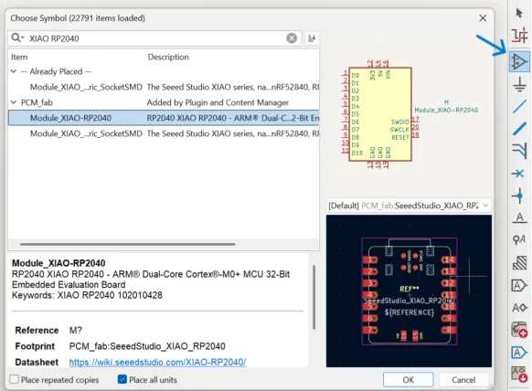
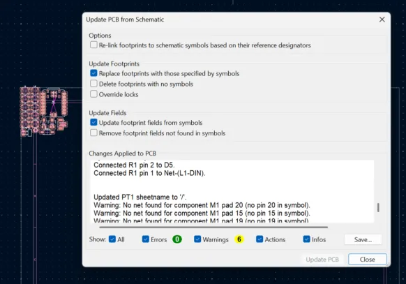
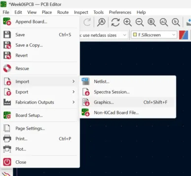
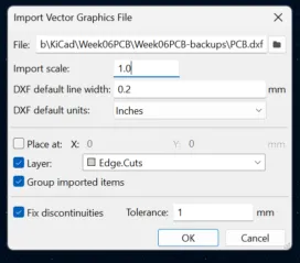
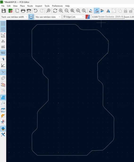
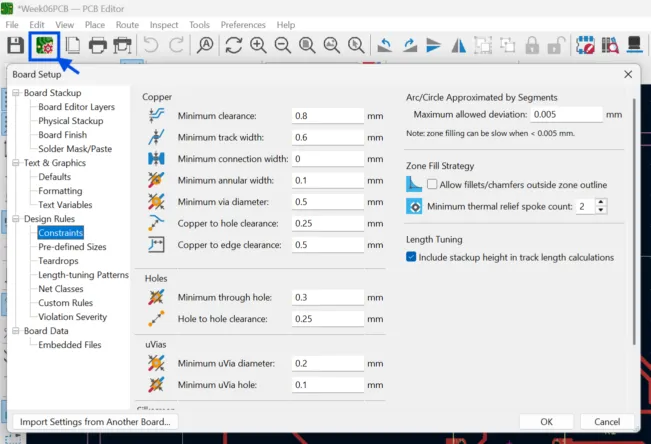
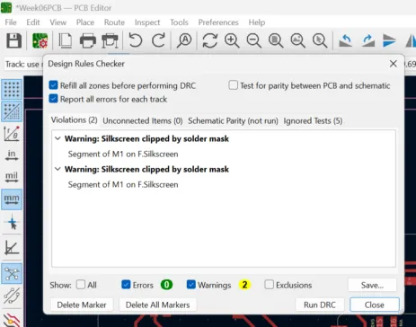
After that we runned a simulation to verify that the circuit worked before fabrication, by checking voltage levels, signal behavior. Then we organized our components using an EDA (Electronic Design Automation) software, in this case I used Ki Cad. Here we routed traces while respecting design rules (trace width, clearance, etc).
To know more about this check the group assignment:
PCB Process
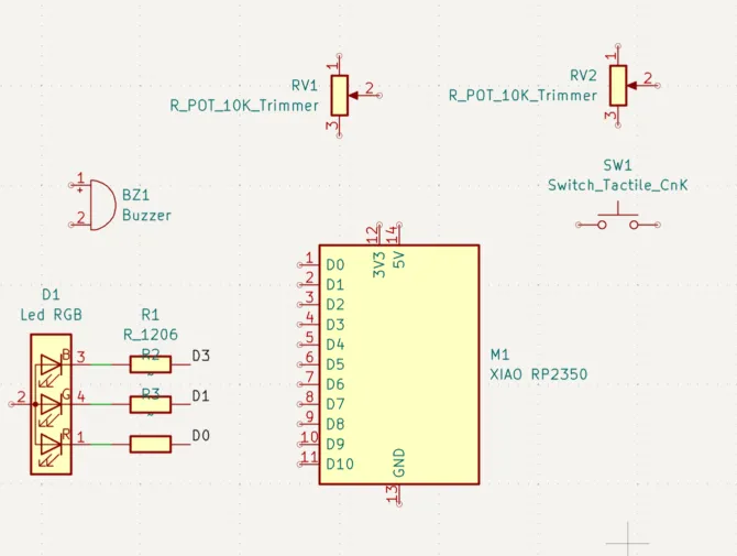
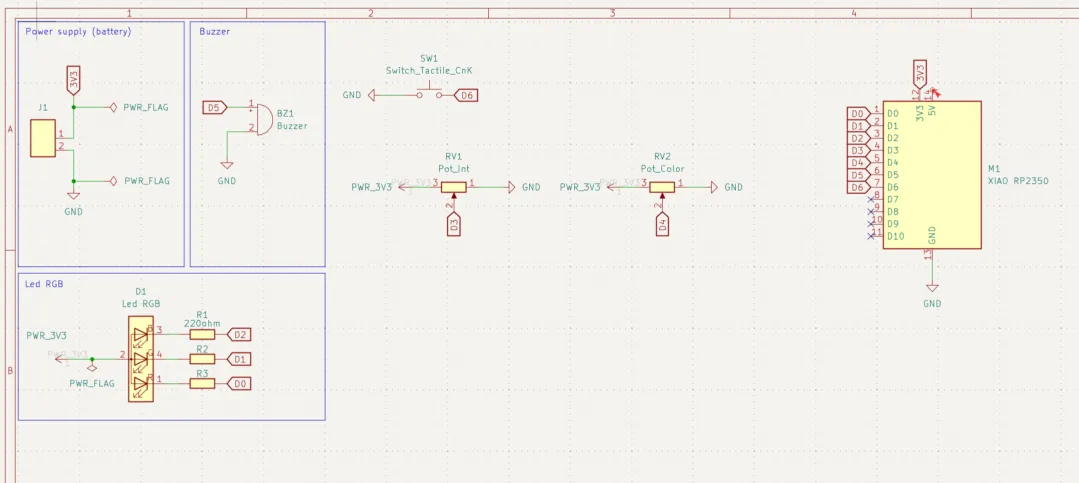
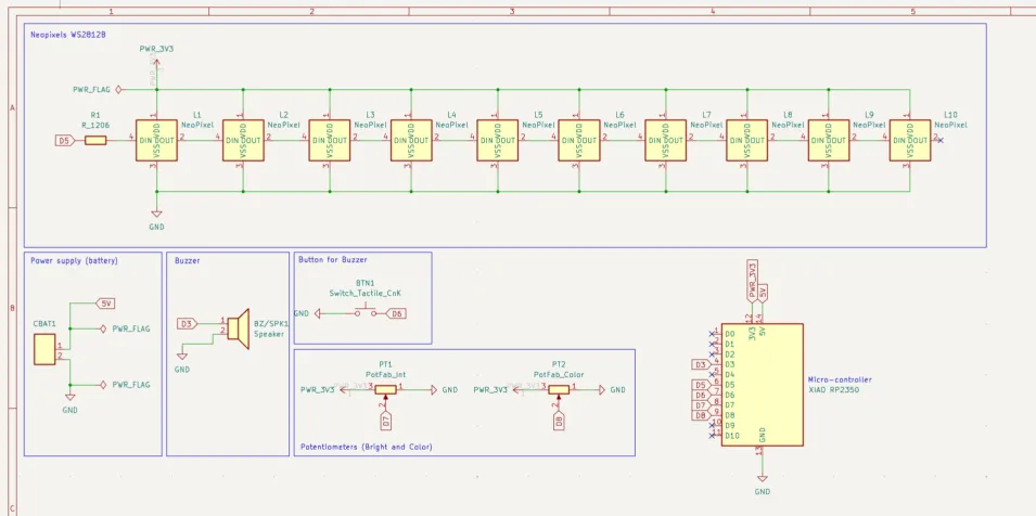
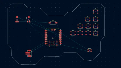
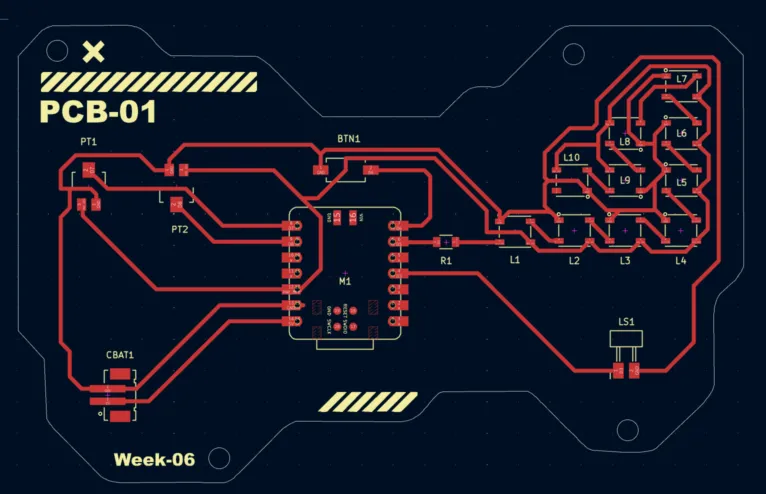
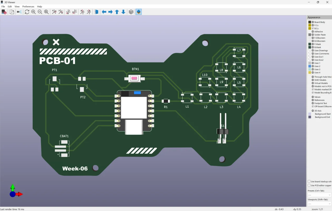
For this exercise I did an interactive lighting and sound control system, that includes a series of WS2812B Neopixels (intelligent RGB LEDs), two potentiometers (one thought for brightness and one to control color), a speaker, a button and a JST PH connector to add a battery.
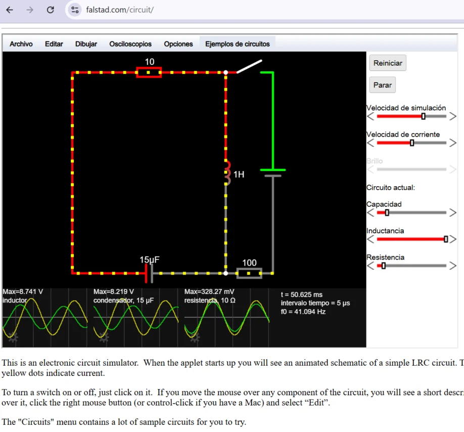
Electronic Simulation on Falstad
Falstad is a browser-based electronic circuit simulator. I chose to use it because it helped me understand voltage and current, by showing the "real" current flow, as well as circuit examples.
1. Go to Falstad web page. At first you will see a circuit example.
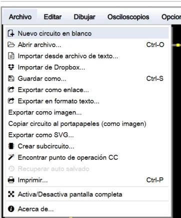
2. Go to file and create a blank new circuit.
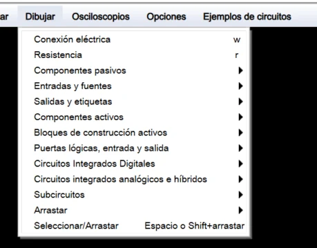
3. Then use draw to create your components symbols (I used a 5V source, 3 leds, 3 resistors, 1 interuptor and GND)
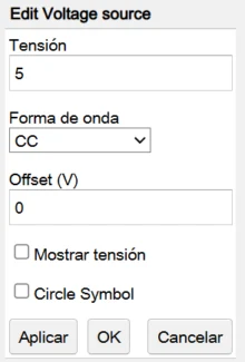
3.1 You can modify the components values. To calculate the resistance I used the Ohm's Law and each LED has different values because some need less voltage (Red consumes less that the Blue LED).
4. Run the simulator and change values if necessary.
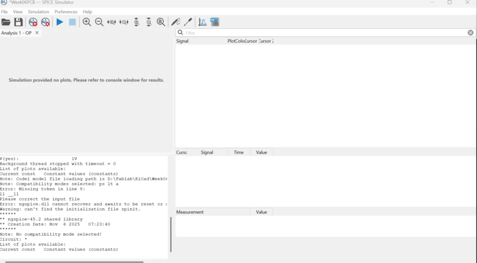
You can also simulate on Ki Cad, although I found it less intuitive.Here is how te simulator window looks (there is no simulation here just the interface).
Learning Outcomes
This week I learned more about electronics components and circuit design by exploring schematics outside of Wokwi. Working with the circuit diagrams and planning PCB layouts helped me understand how each component connects, why resistors are used, and how Ohm’s Law applies to control current safely.
- Understanding component connections: I learned how and why each component is placed in a circuit and how their interaction affects overall functionality. If something is not connecten it will affect the system.
- Applying Ohm's Law and choosing resistances: The Ohm's Lay states that Voltages (V)= Current(I) * Resistance(R). In this exercise it help me select the correct resistor to protect LEDs and regulate current.
- Importance of pin selection: Choosing the right microcontroller pins ensures proper circuit operation and prevents conflicts.
- PCB layout planning: Organizing components and traces carefully prevents wire crossings and improves the future manufacture and welding. For me this was the biggest challenge, specially wiring the LEDs because ended up changing some pins to improve the net.
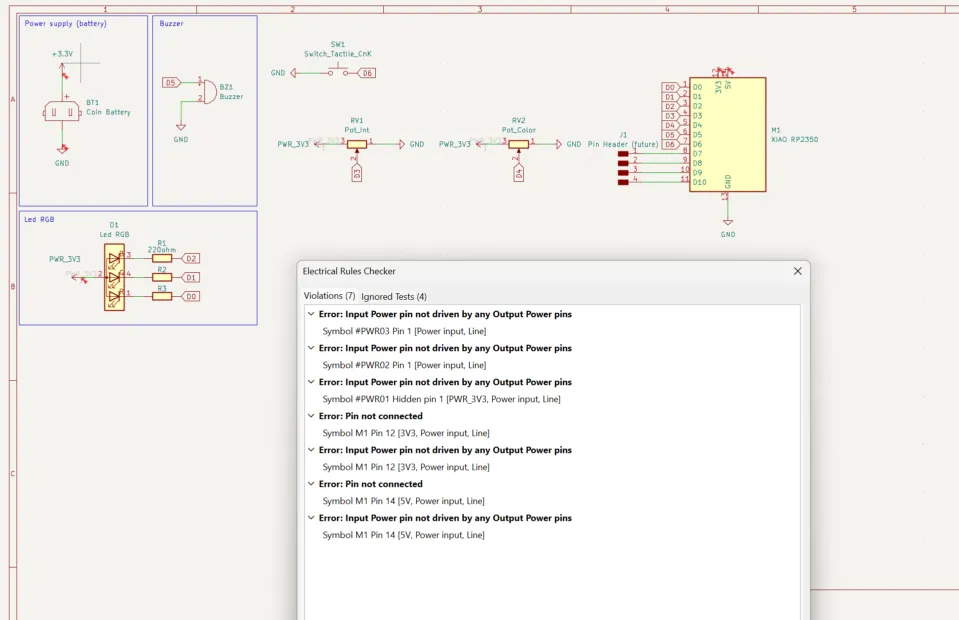
- Running checks: Performing Electrical Rules Check (ERC) and Design Rules Check (DRC) helps detect errors before and while building the PCB.
In future weeks this will help me to plan and design the PCB for my pill dispenser. I tried to add components that I may use on it like the leds, potentiometers and the buzzer.