8. Electronics Production
Group Assignment
This week we focused on two things: characterizing the design rules for our in-house PCB milling process, and submitting a PCB design to a board house.
This week’s work started as a group effort. We characterized the milling process together, which gave me a solid foundation for my individual work. More details on the group assignment can be found here.
Our Setup
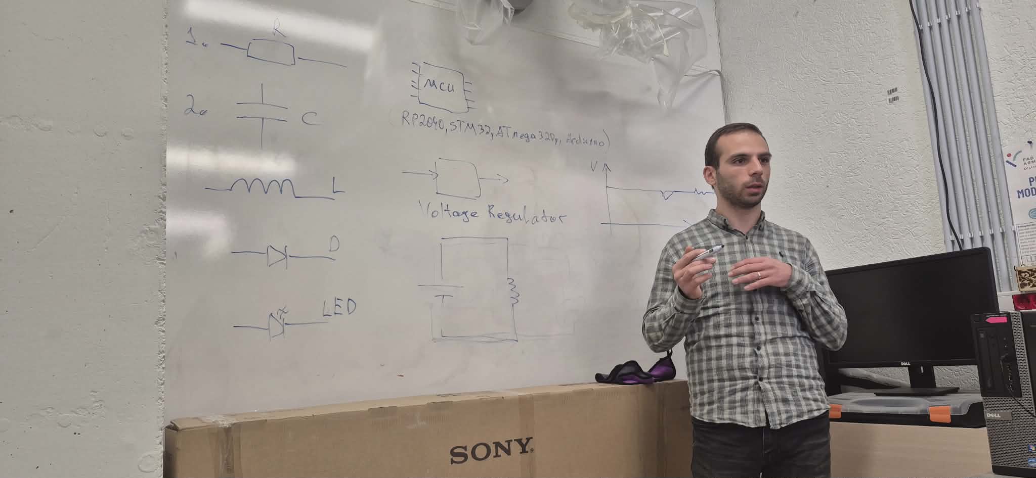
Both the Dilijan and Gyumri labs use the Roland SRM-20 CNC machine for milling PCBs. Before starting the practical work, our instructor Onik Babajanyan walked us through the essential electronic components — resistors, capacitors, LEDs, diodes, MOSFETs, voltage regulators, and transistors — and explained how each one functions in a circuit.
Preparing the Board
To secure the copper board to the MDF bed, we used double-sided tape. The milling depth for traces is only 0.1mm, so even slight warping can cause problems — either not cutting deep enough, or cutting too deep. The tape keeps the board flat and firmly in place.
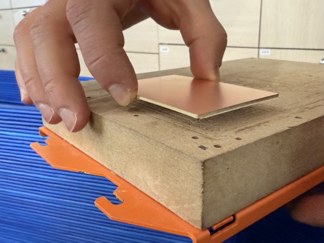
For stronger adhesion, we placed an 18mm plywood sheet on top and clamped it down for 10–15 minutes before starting.
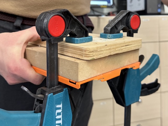
Once the board was secure, we put the removable table back in and fastened it with screws.
Machine Calibration
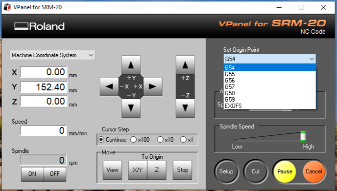
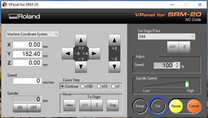
We used VPanel for SRM-20 to control the machine.
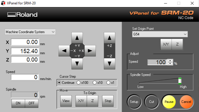
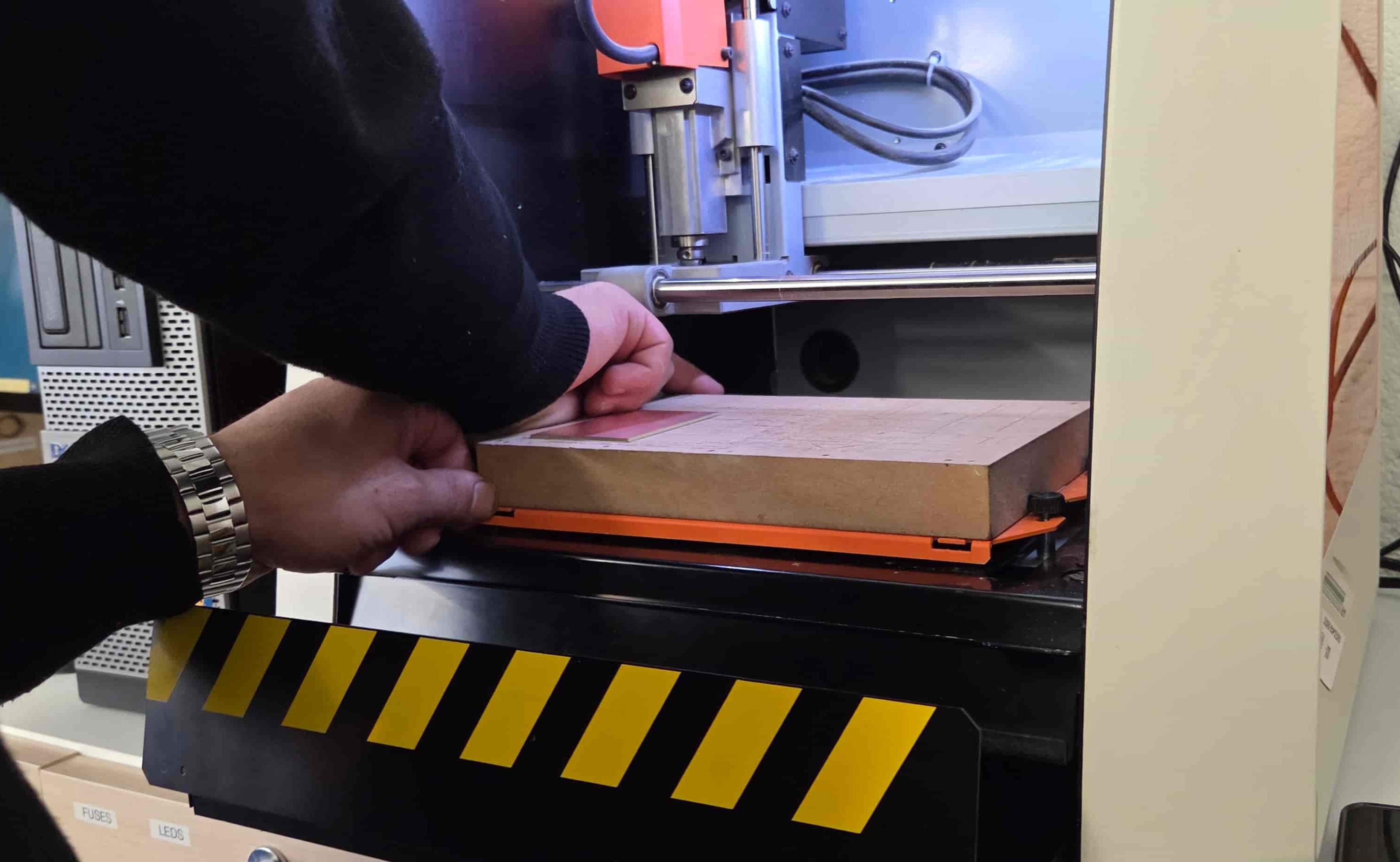
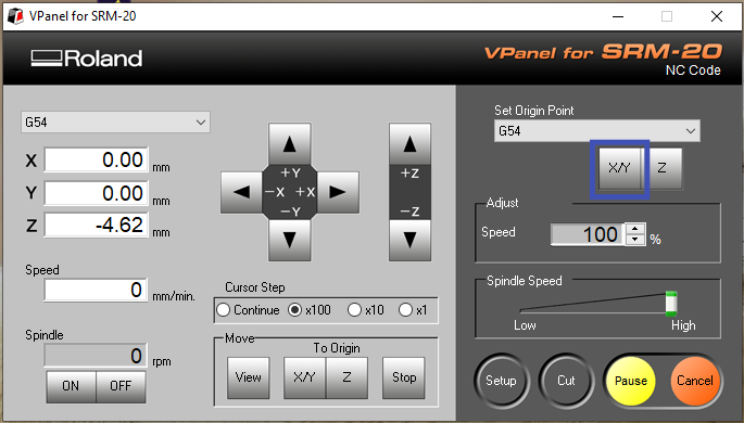
Because the board is replaced almost every session and isn’t always in the same position, XY zero needs to be reset each time. We moved the bit to the bottom-left corner and pressed the X/Y button to set the origin.
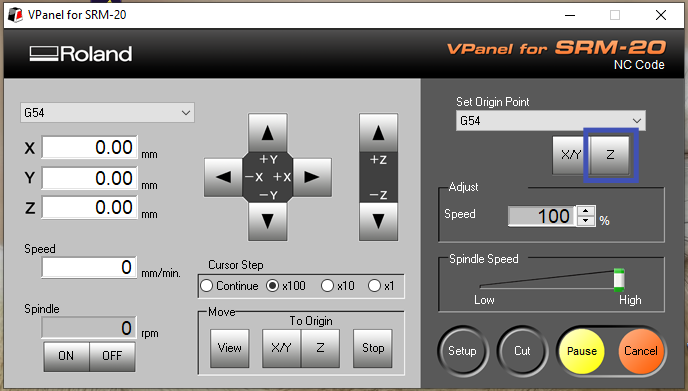
Z calibration is done manually — we lowered the bit close to the surface, released it with a hex key, let it touch the board, then tightened and pressed Z to zero.
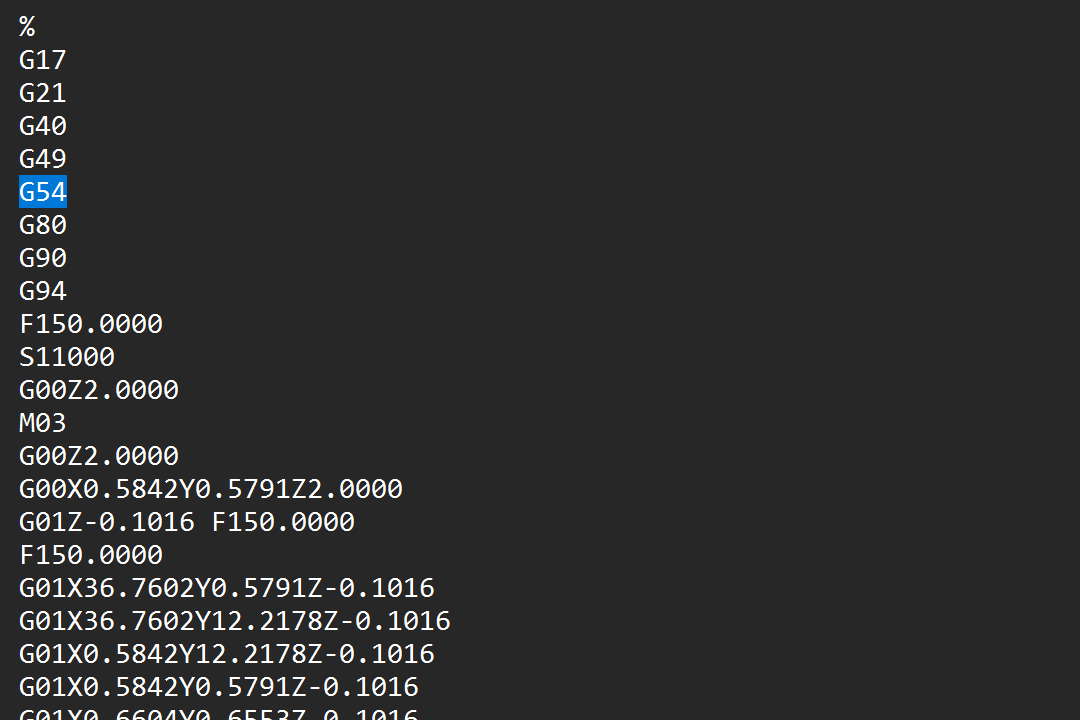
One important detail: when using .nc files, coordinate systems G54–G59 are available. Files generated with modsproject default to G54, so the zeroing needs to match that.
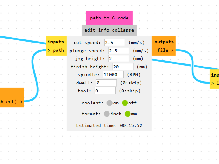
G-code Generation
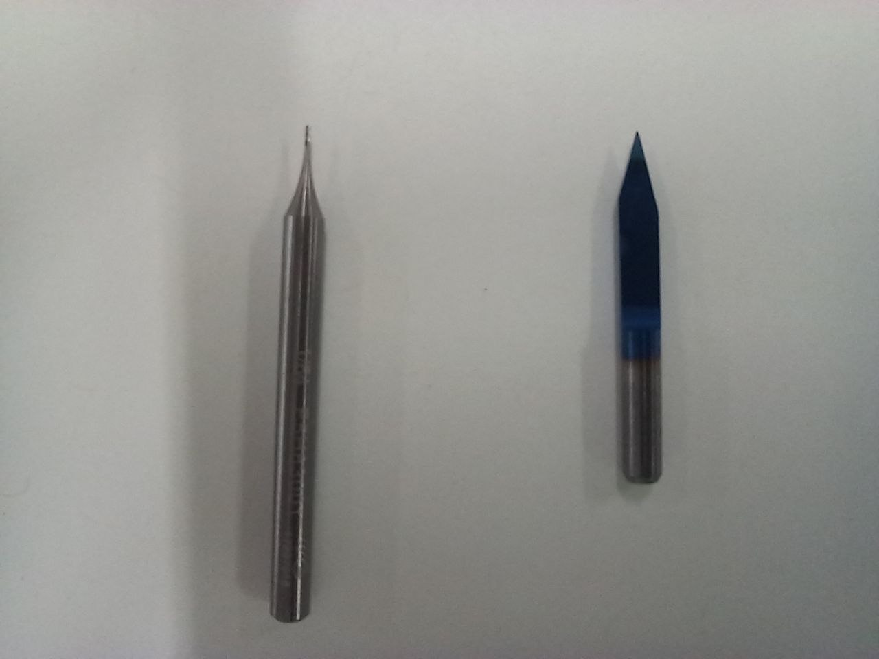
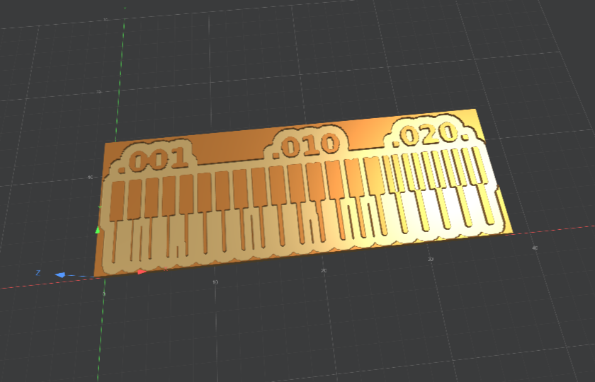
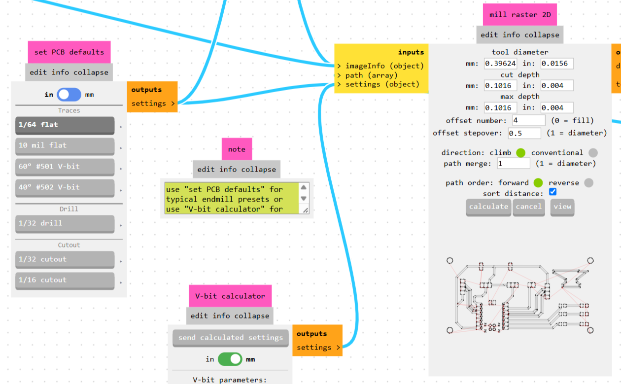
As a test we used the standard Fab Academy line test design. We wanted to compare two bit types: a 1/64” flat end mill and a 30° V-bit.
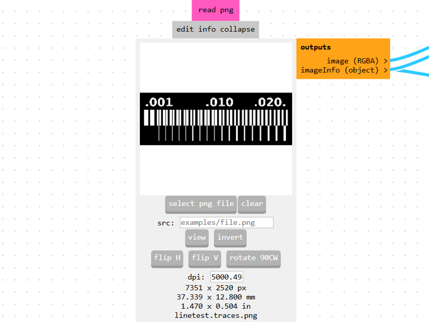
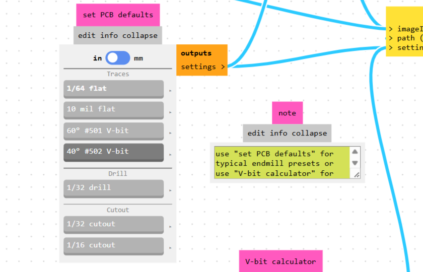
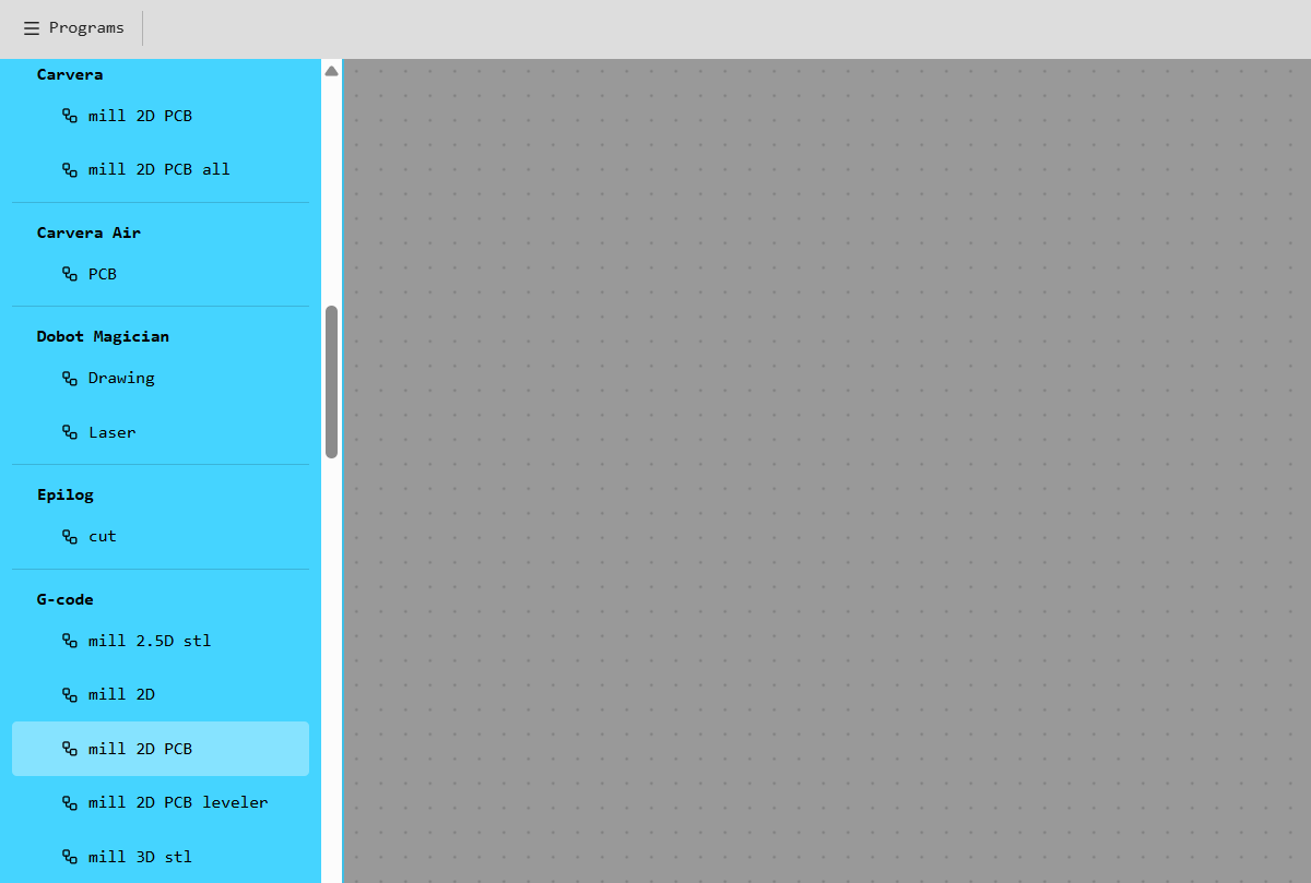
For G-code we used Fab Mods — under Programs → mill 2D PCB. It accepts SVG or PNG input; we used PNG.
Flat End Mill
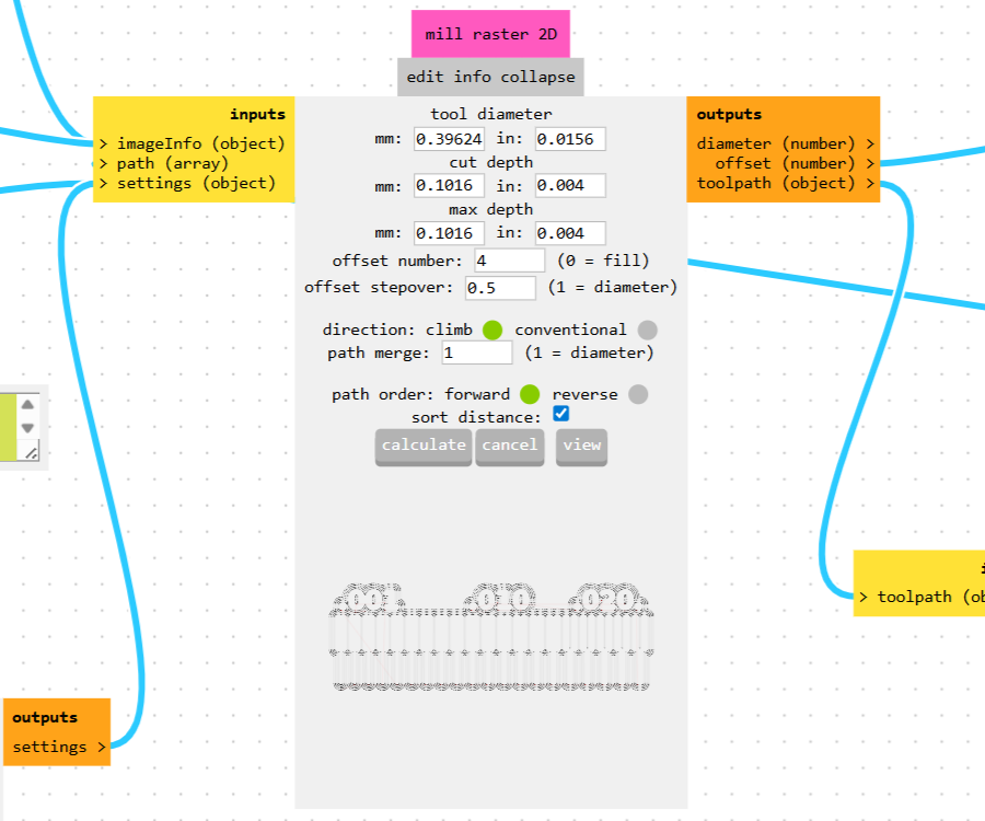
We selected Traces as the operation and set the tool diameter to 0.4mm (metric bits in the Gyumri lab). Max depth was left at 0.1mm — the copper layer is only 0.07mm thick, so that’s enough. Cut depth stayed at 25% of the bit diameter.
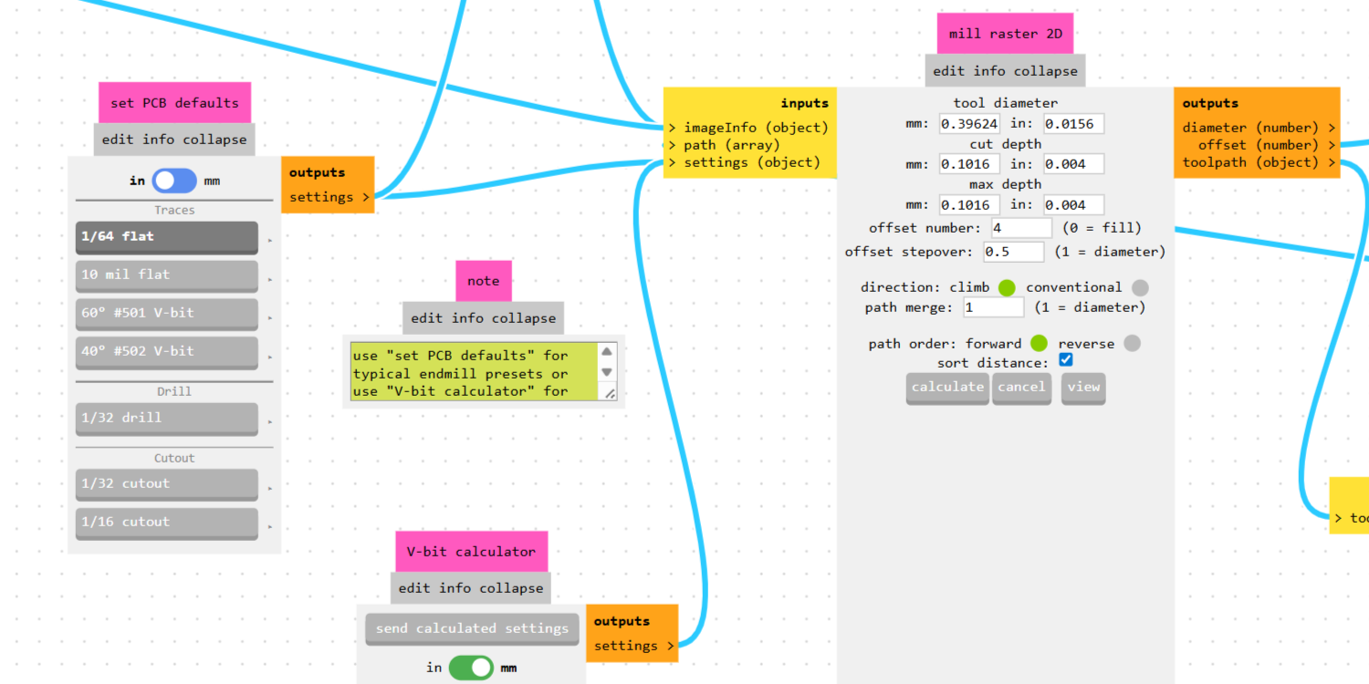
Worth noting: the actual spindle speed doesn’t reach the set value — it runs at around 9000 RPM in practice.
After clicking Calculate, a 3D preview and path visualization appeared before saving the file.
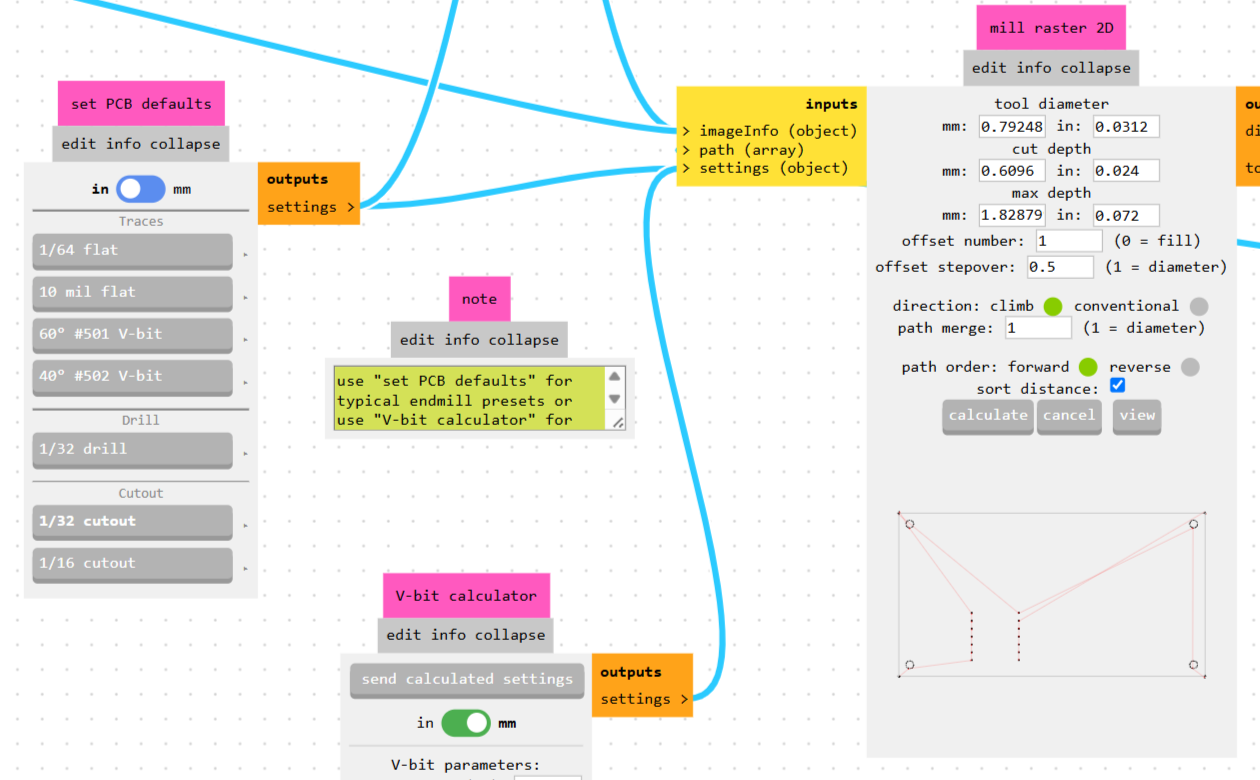
V-bit
The process is the same, but the standard tool options only offer 60° and 40° — our bit is 30°. We used the V-bit calculator, entered a tip diameter of 0.1mm and a 30° angle, set cut depth to 0.1mm, and clicked Send calculated settings.
Milling
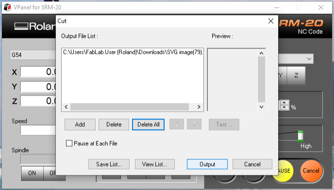
We opened VPanel, clicked Cut, cleared the previous file with Delete All, loaded the new .nc file, and clicked Output.
Results
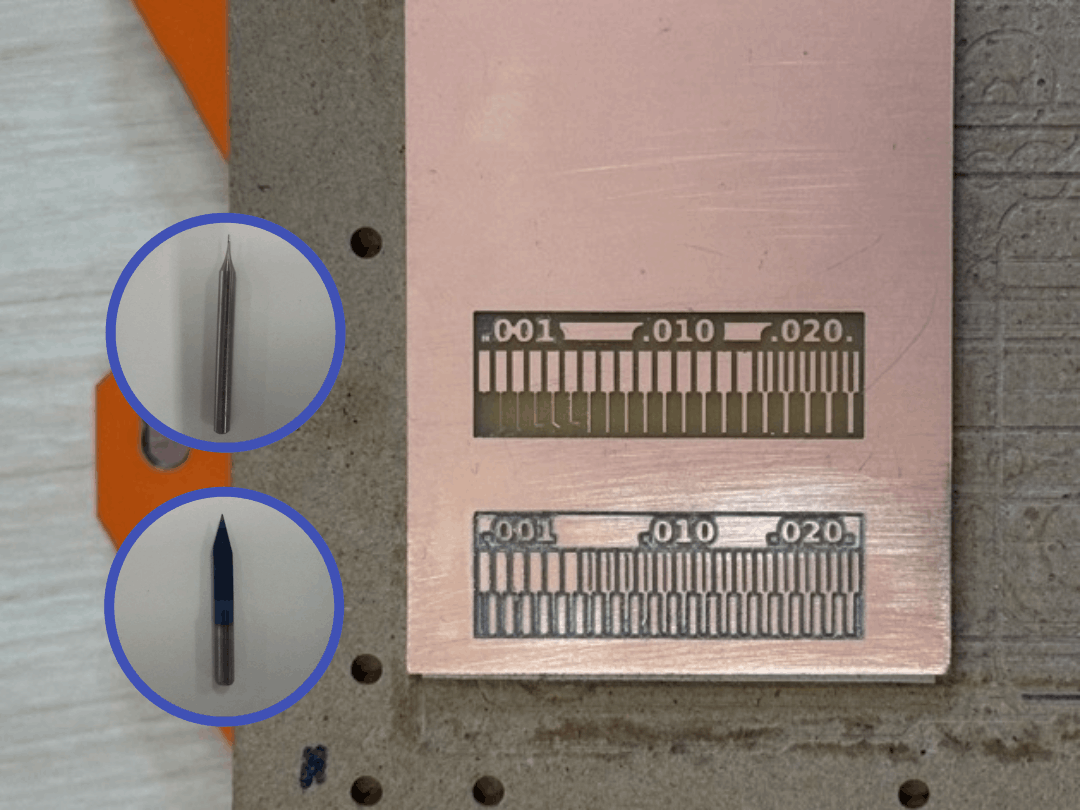
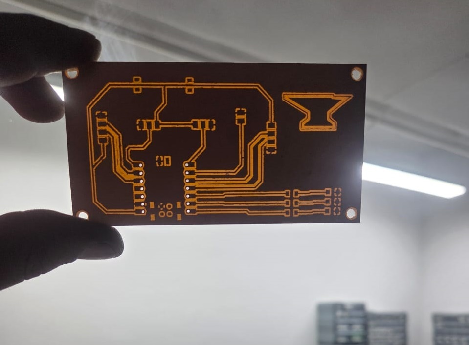
The flat end mill produced clean, well-defined traces across all widths — even the narrowest gaps at 0.001” were clearly separated.
The V-bit results were less consistent. With the offset number set to 4 and a very small tip diameter, some copper areas between passes weren’t fully cleared. We also sanded the V-bit section after milling, which affected how it looks in comparison.
For reliable PCB fabrication, the flat end mill is the clear choice.
Sending a PCB to a Board House
For the group assignment, we also documented the process of sending a PCB design to a board house, using PCBasic as an example.
We uploaded a board design (1 layer, 32.4 × 77.4 mm, FR4 material, 1.6 mm thickness) and requested a quote for 10 pieces.
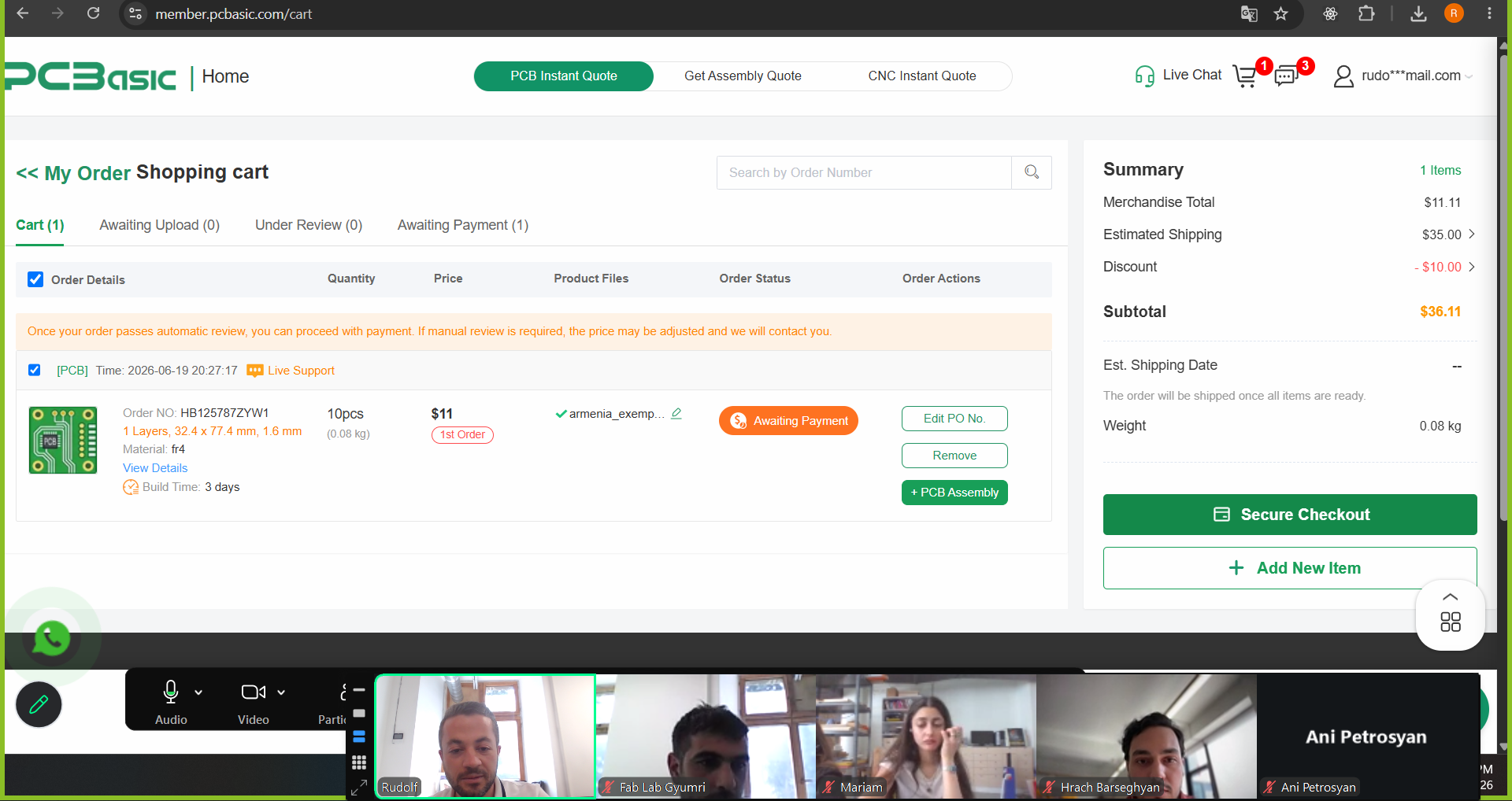
The site automatically reviewed the file, gave us a price of $11 for the order with an estimated 3-day build time, and the order reached the Awaiting Payment stage in the cart.
We stopped here without completing the purchase, since we don’t actually need this PCB manufactured — the assignment only requires documenting the workflow up to the final payment step, not placing the order.
Individual Assignment
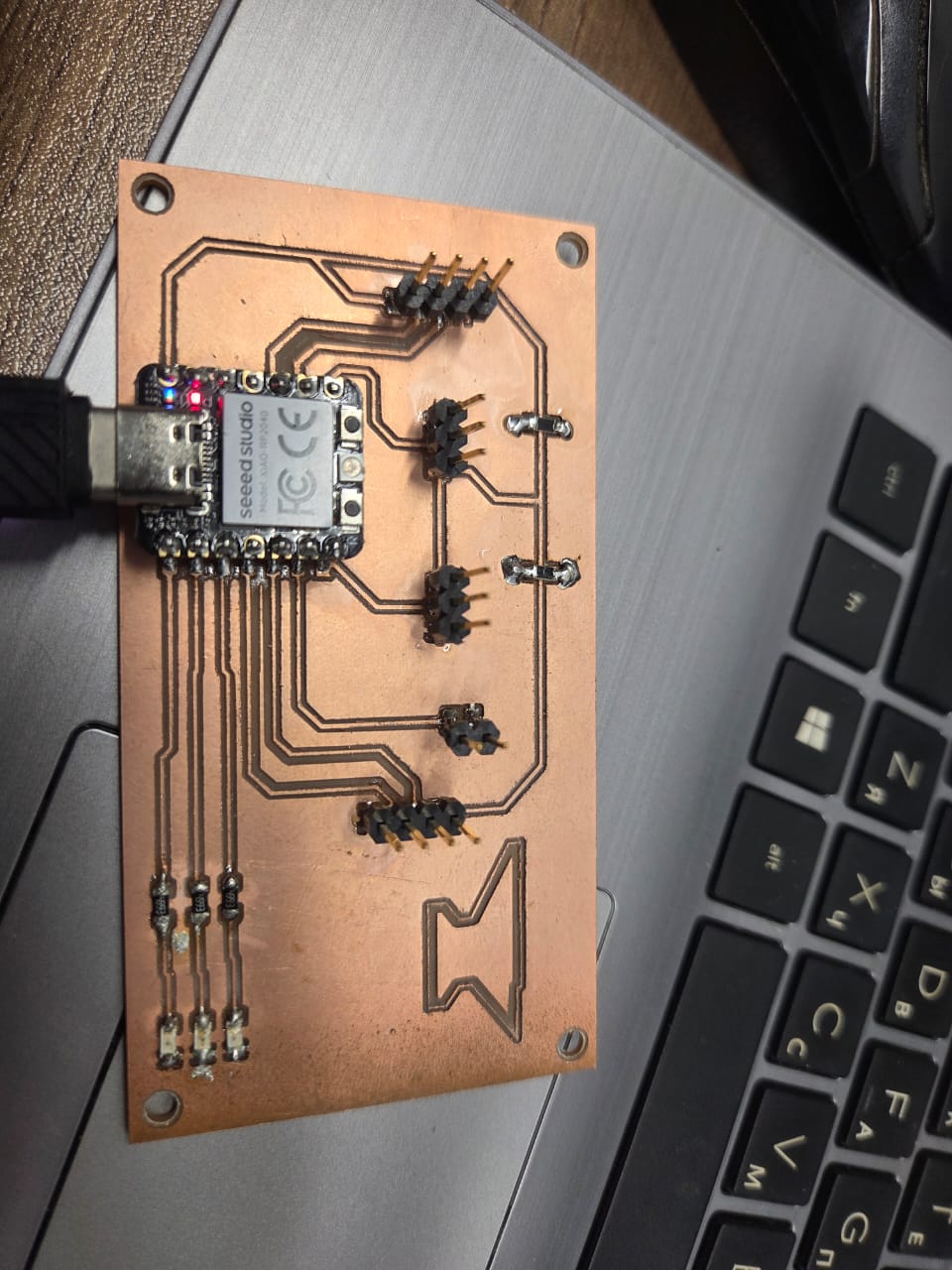
For this assignment, I milled and soldered the board I had designed in Week 6 — the board built around the XIAO RP2040, with pin headers for the gas sensor, a buzzer, three status LEDs, and a few spare pins.
Exporting the Design
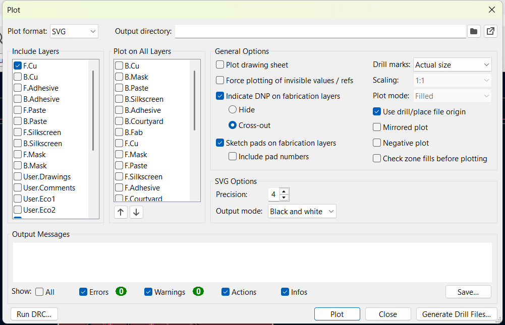
Before generating any toolpaths, I needed to export my design from KiCad as SVG files. In the PCB Editor, I went to File > Fabrication Outputs > Gerbers (.gbr), set the plot format to SVG, and made sure only the layers I actually needed were checked: F.Cu (the copper traces) and Edge.Cuts (the board outline and mounting holes). I exported each of these as a separate file, since they need different milling bits later.
Generating the Toolpath
I used Fab Mods to generate the G-code, the same way as in the group milling characterization — under Programs, selecting mill 2D PCB.
For the traces, I loaded the F.Cu SVG file. By default, the copper areas that should remain show up as the background, and the gaps between traces show up as the shape — which is the opposite of what the mill needs to cut. So before generating the path, I applied the invert function, which flips this so the mill correctly removes copper between the traces instead of cutting away the traces themselves.
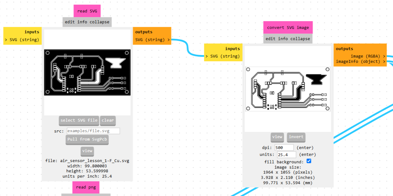
After inverting, I selected the 1/64” flat end mill — based on the group test, this bit gave cleaner results than the V-bit — and generated the toolpath.
For the board outline and the mounting holes, I loaded the Edge.Cuts SVG separately. This file doesn’t need to be inverted, since it’s just the cut line itself, not a copper pattern. I generated a second toolpath here with a larger bit, since the outline doesn’t need the same fine resolution as the traces.
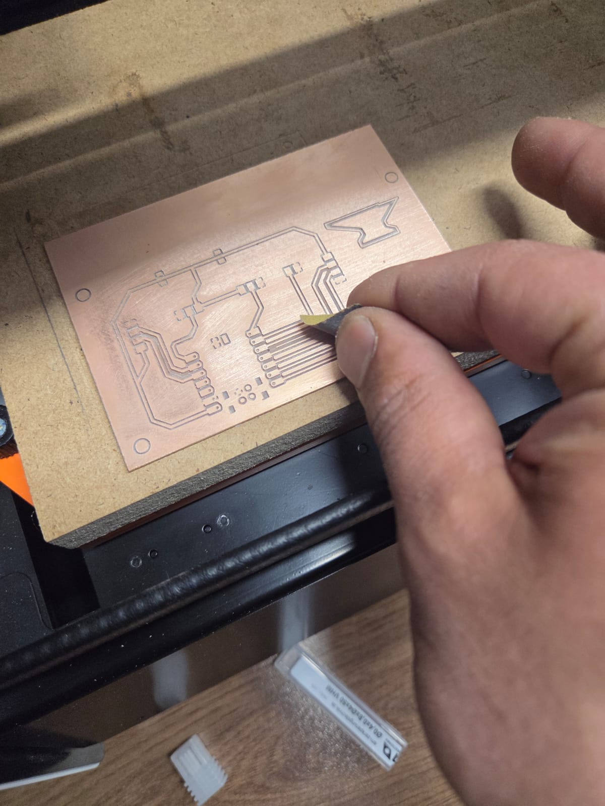
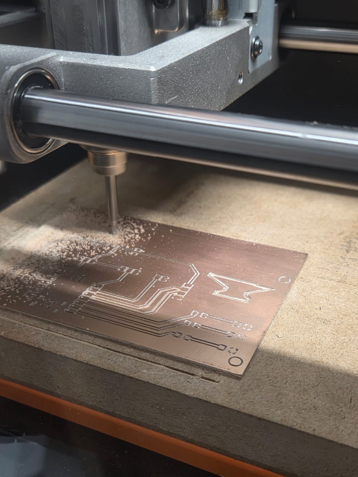
Milling
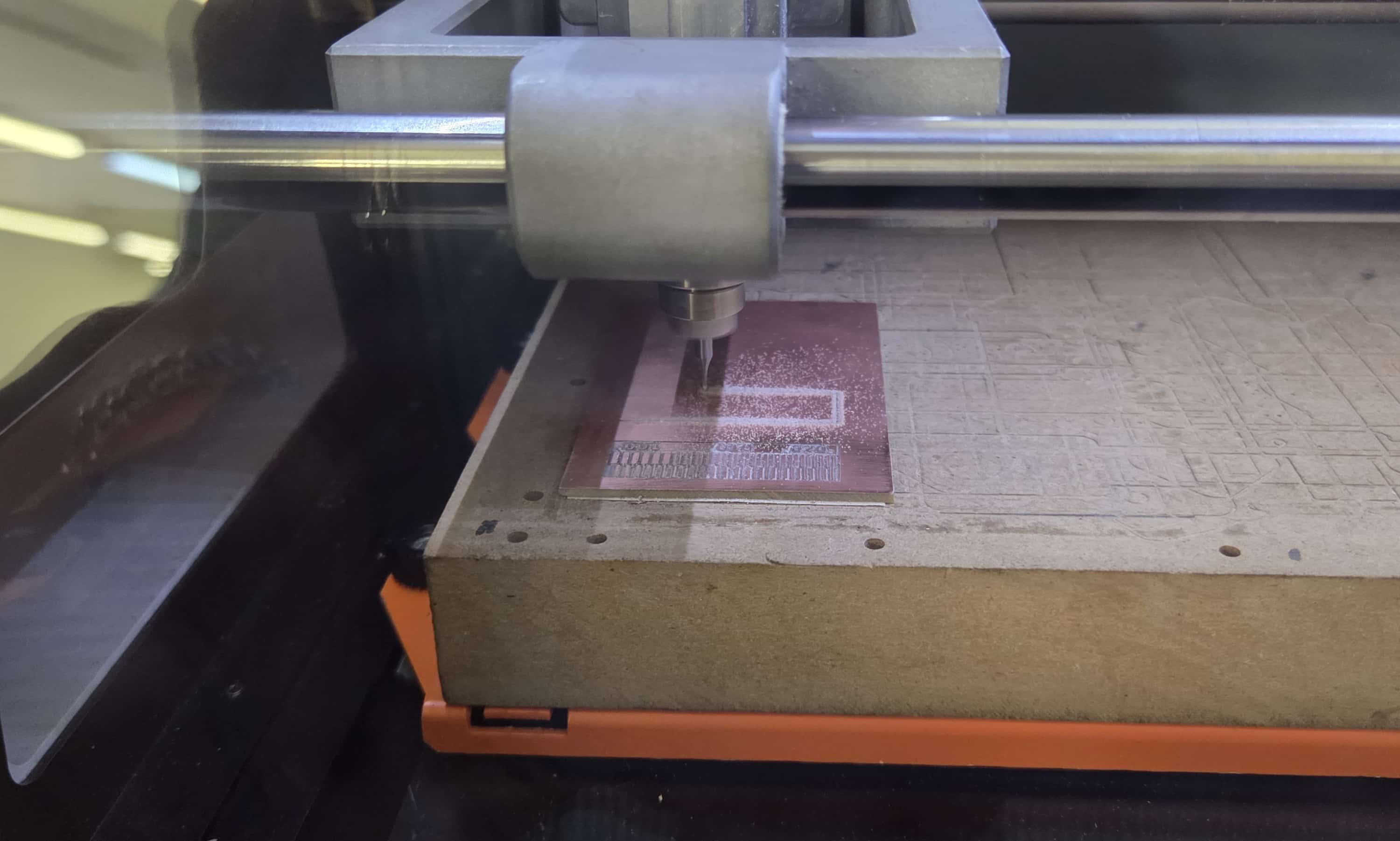
I taped my copper board to the SRM-20 bed the same way as during the group test, zeroed the X/Y and Z axes, and ran the traces file first.
The traces came out cleanly after milling.
After that, I changed to the larger bit, re-zeroed the Z axis, and ran the outline file to cut the board shape and the mounting holes.
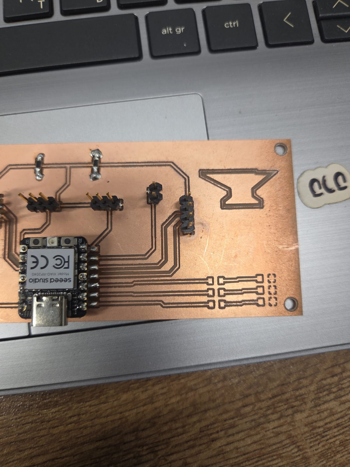
Here is the board after both milling passes were complete — traces and outline cut — before any soldering:
Soldering
Once the board was milled, I soldered on the components. The three SMD LEDs and their resistors went directly onto the board, along with the pin headers.
Components used:
| Component | Quantity | Notes |
|---|---|---|
| Seeed Studio XIAO RP2040 | 1 | Microcontroller |
| SMD LED 1206 | 3 | Red, Yellow, Green |
| Resistor 1kΩ 1206 | 3 | Current limiting for LEDs |
| Pin header 2-pin | 4 | Sensor and buzzer connectors |
| Pin header 3-pin | 2 | Sensor connectors |
| Pin header 4-pin | 1 | I2C connector |
| DC barrel jack (2x5.5mm) | 1 | 12V power input |
| NCP1117 voltage regulator SOT-223 | 1 | 12V to 5V |
Soldering setup and tools:
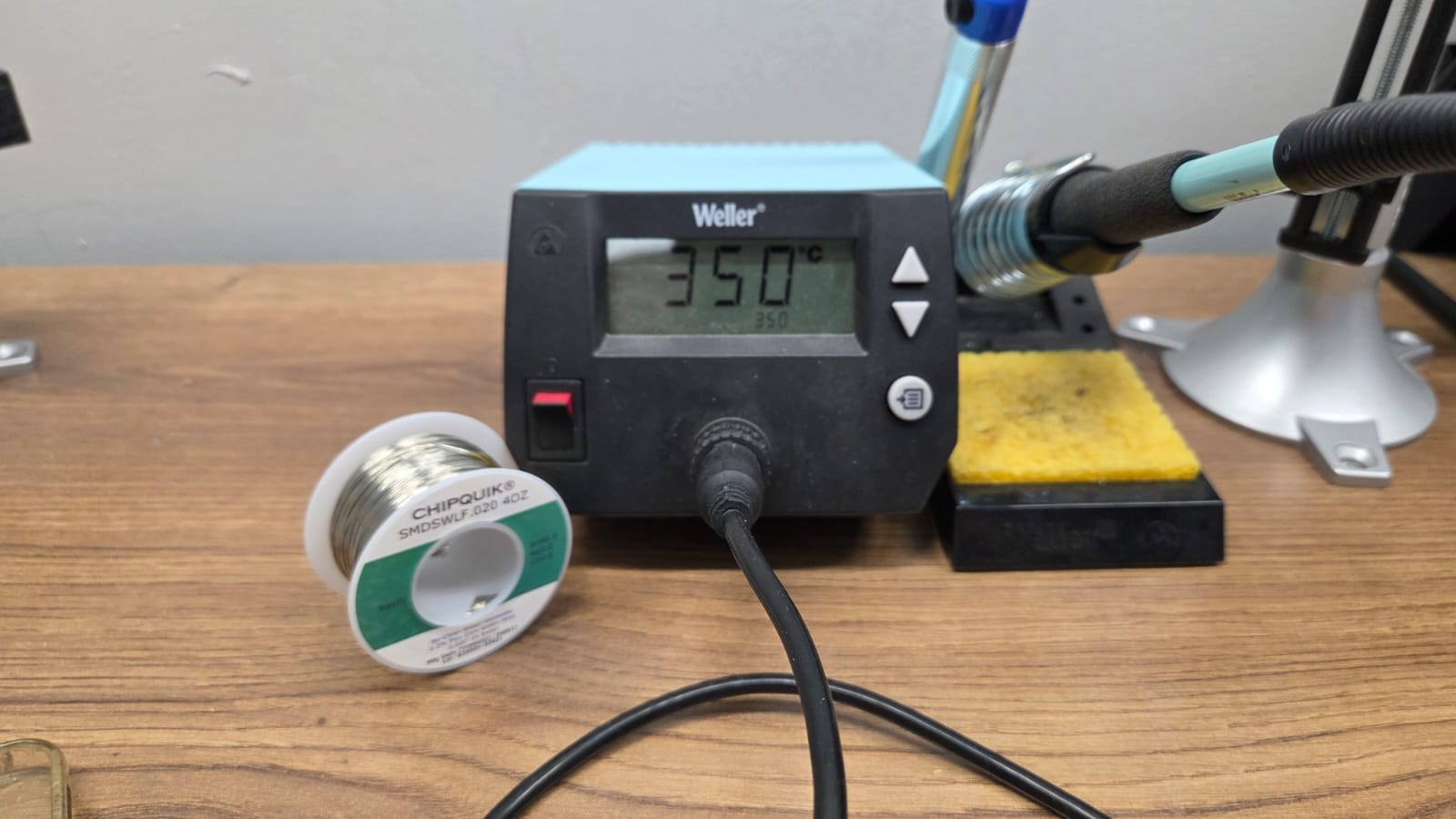
- Weller soldering station — temperature set to 350°C
- Chipquik SMDSWLF.020 solder — lead-free, 0.5mm diameter
- Tweezers — for placing SMD components
- Flux — for cleaner joints on SMD pads
- Microscope/magnifier — for inspecting small SMD pads
I didn’t solder the gas sensor or the other external sensors directly onto the board — instead, since those connect through pin headers, I’ll wire them externally with jumper wires whenever I need them, rather than fixing any specific sensor permanently to the board.
I didn’t run into the ground plane routing issue some of my classmates had (the one usually solved with 0 Ω bridge resistors) — my GND zone routed cleanly without needing any bridges.
Testing
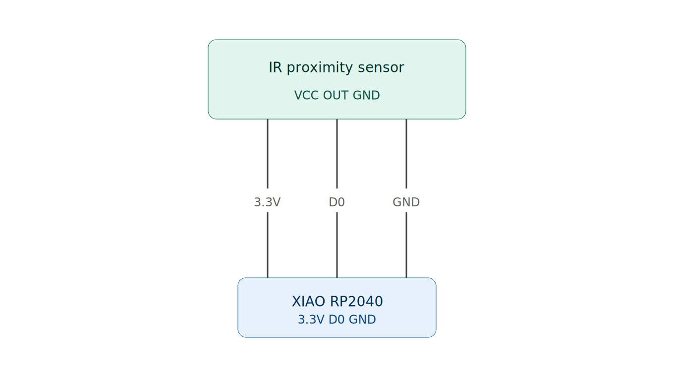
The board is powered directly through the XIAO RP2040’s USB connector. To check that it was working, I connected an infrared obstacle sensor to one of the spare GPIO pins and wrote a small program so the board’s LEDs would react to it: green LED on by default, switching to the yellow and red LEDs blinking when the sensor detected an object in front of it.
The wiring follows the same setup I first tested in Week 4 — VCC to 3.3V, GND to GND, and the signal output to a digital GPIO pin.
AI prompt used:
“Write Arduino code for XIAO RP2040 that reads a digital IR obstacle sensor on pin D0. Keep the green LED on pin D3 on by default. When the sensor detects an object (HIGH), turn off the green LED and blink the yellow (D2) and red (D1) LEDs alternately every 200ms.”
Test code:
#define IR_PIN     D0  // IR sensor signal pin
#define LED_GREEN  D3  // green = safe / no detection
#define LED_YELLOW D2  // yellow = warning blink
#define LED_RED    D1  // red = warning blink

void setup() {
  pinMode(IR_PIN, INPUT);          // sensor input
  pinMode(LED_GREEN, OUTPUT);
  pinMode(LED_YELLOW, OUTPUT);
  pinMode(LED_RED, OUTPUT);
  digitalWrite(LED_GREEN, HIGH);   // default: green on
}

void loop() {
  if (digitalRead(IR_PIN) == HIGH) {  // object detected
    digitalWrite(LED_GREEN, LOW);
    digitalWrite(LED_YELLOW, HIGH);
    delay(200);
    digitalWrite(LED_YELLOW, LOW);
    digitalWrite(LED_RED, HIGH);
    delay(200);
    digitalWrite(LED_RED, LOW);
  } else {                             // no object
    digitalWrite(LED_GREEN, HIGH);
    digitalWrite(LED_YELLOW, LOW);
    digitalWrite(LED_RED, LOW);
  }
}
This confirmed that the USB power path, the GPIO pin I used for the sensor, and the LED outputs were all working correctly on the board.