6. Electronics Design
Group Assignment
This week’s group assignment was to use the lab’s test equipment to observe the operation of an embedded microcontroller — at minimum, using a logic analyzer.
We used a GW Instek GDS-1152A-U oscilloscope (150 MHz bandwidth, 2 channels, 1 GSa/s sampling) to look at signals coming from an XIAO RP2040.
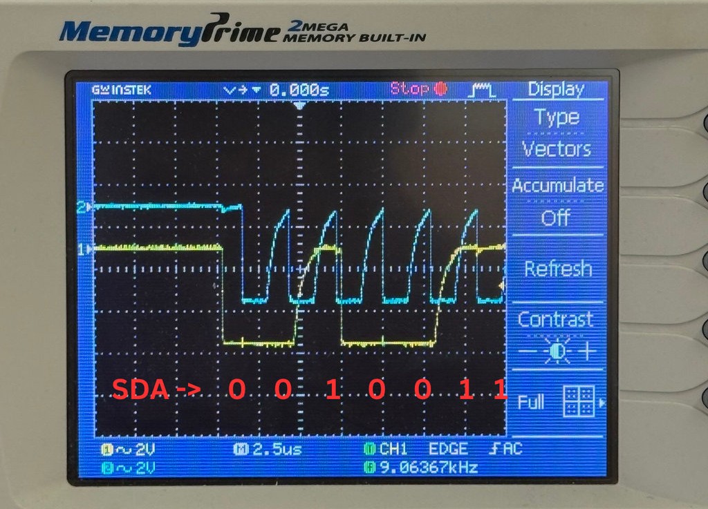
First, we probed the I2C lines (SDA/SCL) while the RP2040 was sending data to an LCD, and read the signal timing directly off the screen. It was really interesting for me to actually see what a digital signal looks like on screen, instead of just imagining it from code.
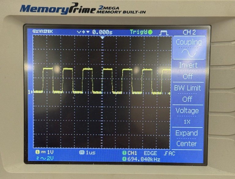
We also ran a simple pin toggle test to see how fast the microcontroller’s main loop could run, comparing MicroPython against C++.
More details on the full setup and code are on the group assignment page.
Individual Assignment
This week I designed my own PCB from scratch. My instructor Rudolf Igityan helped me a lot along the way, especially by walking me through how he had approached his own board design in a previous Fab Academy cycle.
The Board
My goal was to design a small monitoring board built around the XIAO RP2040, which would be powered through its USB port. The board needed to:
- Read a CO/CO2 gas sensor (I’m planning to use an MQ-2)
- Drive a buzzer that turns on if the gas reading goes above a set threshold
- Drive 3 SMD 1206 LEDs (green, yellow/orange, red) to show the reading level: green for normal, orange for elevated, and red — together with the buzzer — for a dangerous level
- Expose a few spare microcontroller pins through pin headers, so the board could also be reused for other sensors later
Install KiCad
I started by installing KiCad, the free and open-source EDA software for designing schematics and PCBs.
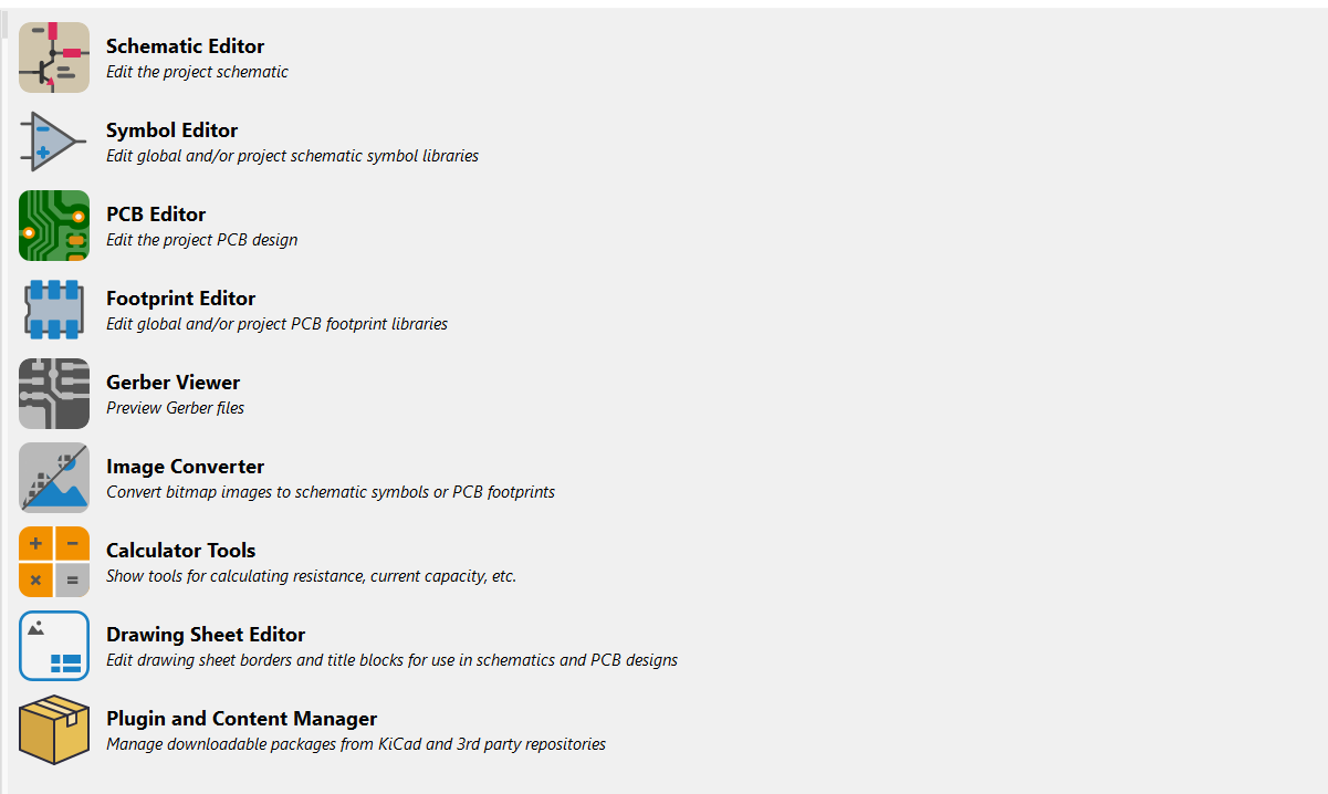
The software offers a wide range of features, but for the purposes of this assignment, I worked with two of them: Schematic Editor and PCB Editor.
Installing KiCad FabLib
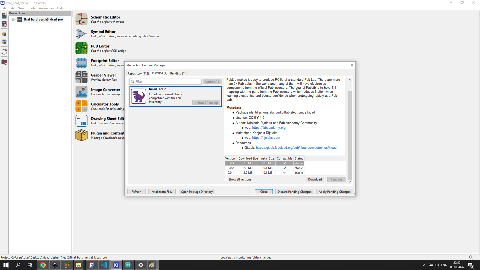
To access the standard Fab Academy component footprints, I installed the KiCad FabLib plugin through the Plugin and Content Manager (Tools → Plugin and Content Manager). I searched for “fab” and found the KiCad FabLib — a component library compatible with the Fab Inventory, maintained by the Fab Academy community.
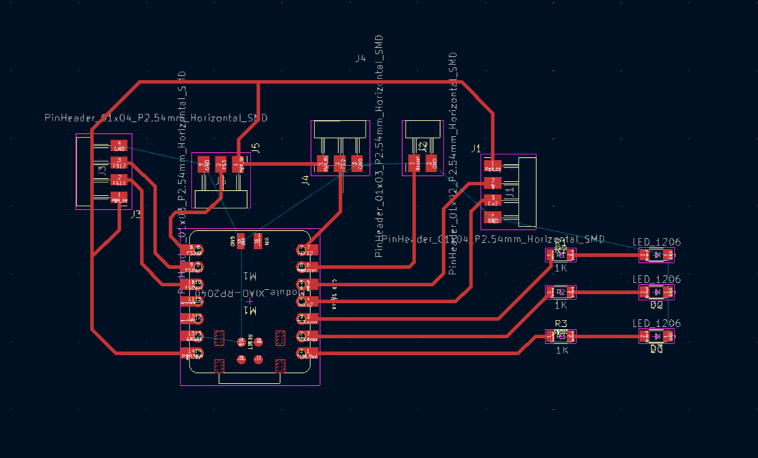
Schematic Design
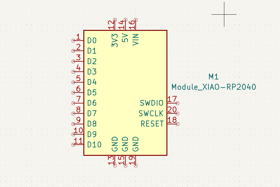
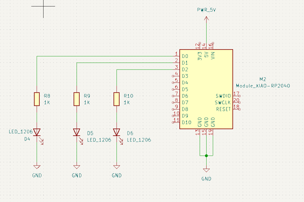
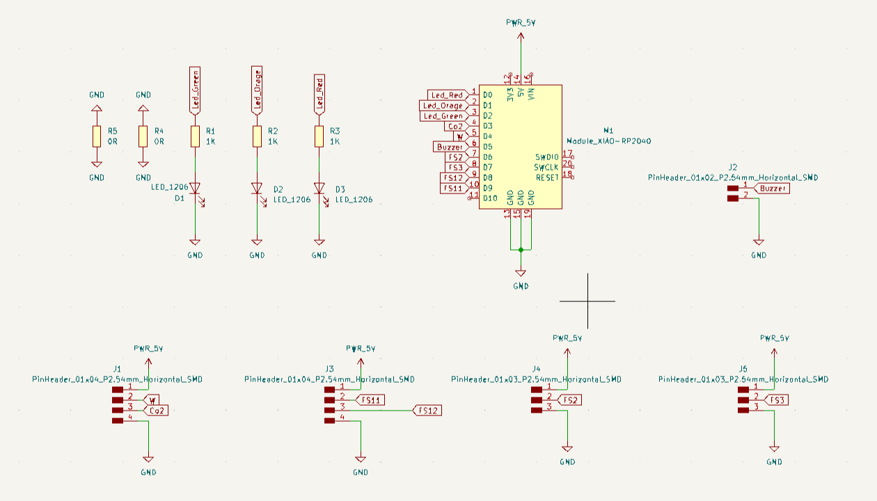
I opened the Schematic Editor and started by placing the XIAO RP2040 module, since it’s the controller everything else connects to.
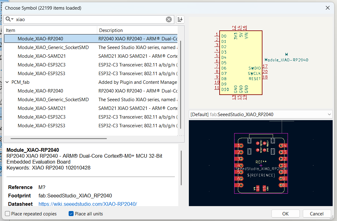
To add a component, I pressed A (or used Place > Add Symbol), searched for the part, and selected it from the list. When a component is found, KiCad also shows its footprint in a small preview window before placing it — this is useful to check that you’re picking the right physical package before it gets added to the schematic.
For all the external sensors, I didn’t add the sensor itself as a schematic symbol — instead, I added pin headers, so that the sensors could be connected externally with wires or a small breakout board. This applies to the gas sensor and to the spare pins. The LEDs, on the other hand, are SMD components soldered directly onto the board, so those I did add as real components.
Power and Ground
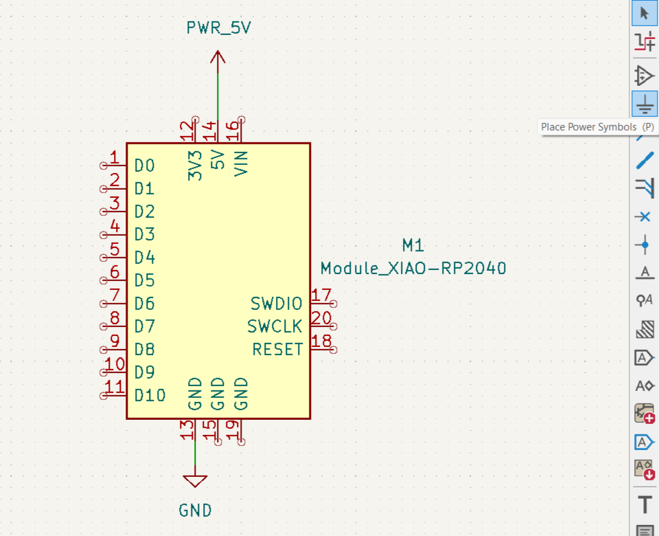
The XIAO RP2040 is powered through its USB connector, so no separate voltage regulator was needed on my board — I just had to bring out 5V and GND to the pin headers that needed them.
LEDs and Current-Limiting Resistors
Each LED (green, orange, red) is driven directly from a microcontroller pin, not from a separate 5V line. The XIAO RP2040’s GPIO pins output 3.3V, so that’s the voltage I used for the resistor calculation.
Looking at a typical SMD 1206 LED datasheet, the forward voltage is around 2.2V, with a recommended current of about 20 mA.
The voltage that needs to be dropped across the resistor is:
U = 3.3V - 2.2V = 1.1V
Using Ohm’s law:
R = U / I = 1.1V / 0.02A = 55 Ohm
The closest standard resistor value I had available was 100 Ohm, which is higher than the calculated 55 Ohm. This means the LEDs run dimmer than their rated brightness, but since these are just status indicators (not meant to be very bright), that’s not a problem for this board — if needed later, I can swap in a lower-value resistor.
Each LED’s resistor connects to GND on the other side:
GPIO pin → Resistor (100 Ohm) → LED → GND
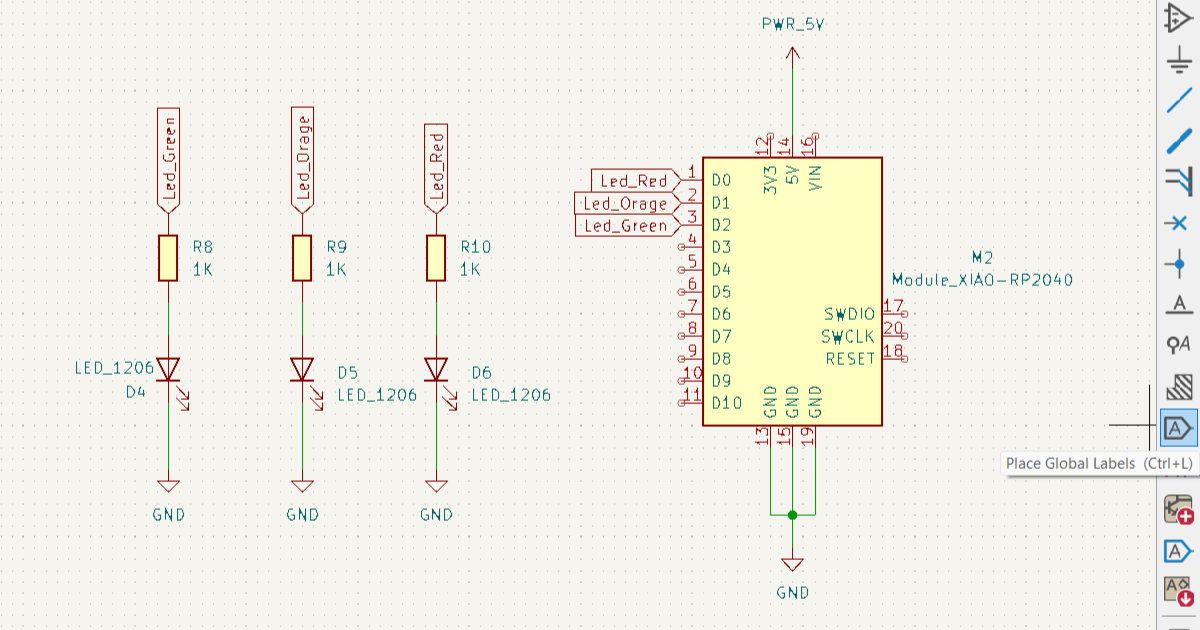
To avoid confusion in the future when placing tracks on the diagram, I used the Place Global Labels tool and gave them names according to what they are connected to, for example Led_Green.
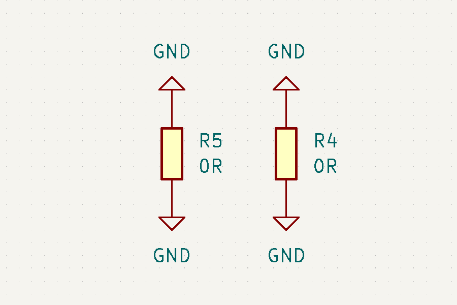
The Two 0 Ohm “Bridge” Resistors
While laying out the PCB later, I ran into a routing problem: the GND zone (the filled copper area connected to ground) got interrupted by traces crossing over it, breaking the ground plane into disconnected islands.
To fix this without adding extra wires on top, I added two 0 Ohm resistors (R4, R5) next to the green and orange LED resistors. A 0 Ohm resistor doesn’t do anything electrically — it acts purely as a bridge, letting a trace “jump over” a gap in the GND zone on the same layer, reconnecting the two separated parts of the ground plane.
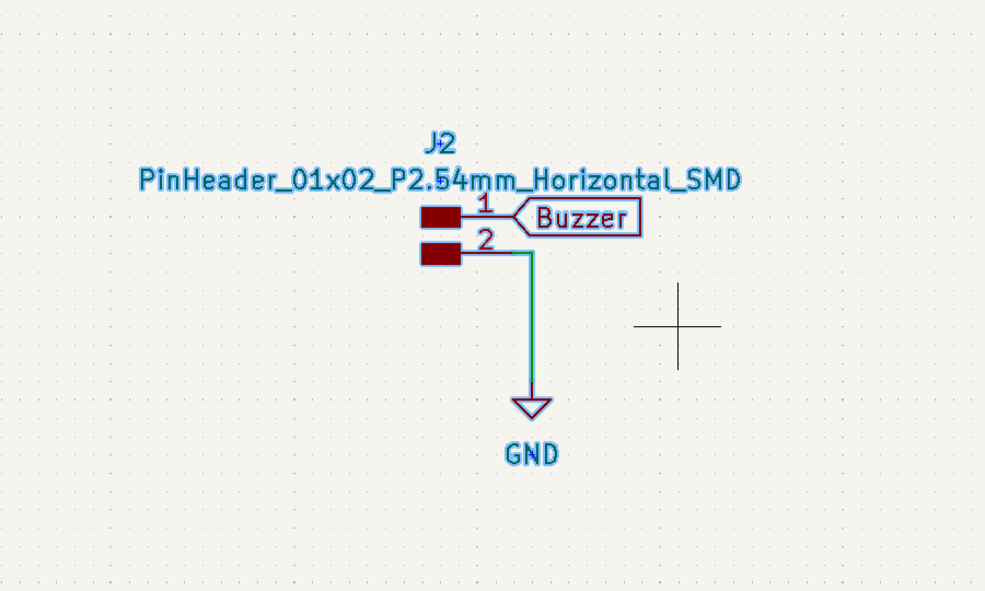
Buzzer
The buzzer needs a PWM signal to produce sound, so it’s connected to one of the XIAO’s GPIO pins (through a 2-pin header, J2) plus GND — no separate power line was needed for it.
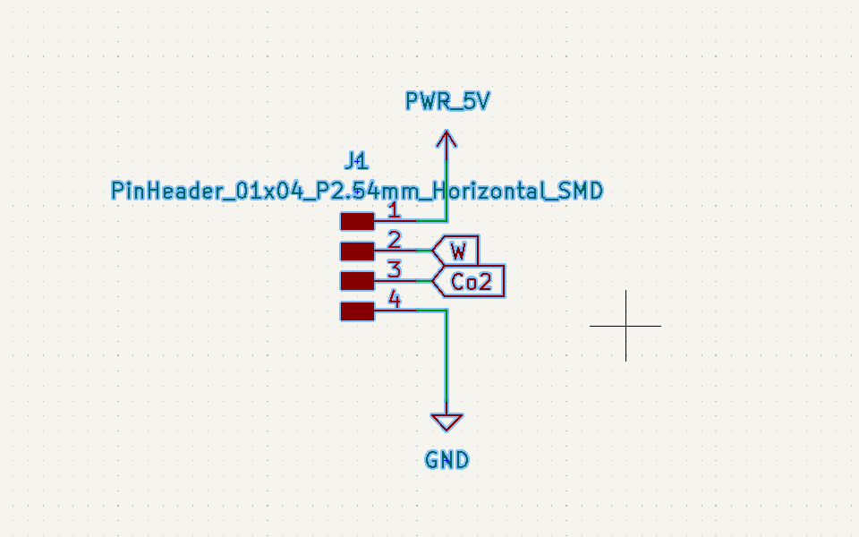
Gas Sensor Header
For the MQ-2 sensor, I wasn’t sure in advance whether I’d end up using its analog output or its digital output (most MQ-series sensors have both), so I left two signal pins broken out to the header instead of committing to just one. That way I can decide later, once I actually test the sensor, which output works better for my threshold logic.
The MQ-2’s heating element needs 5V, so this pin header also carries the +5V line, taken from the XIAO RP2040’s own 5V pin, plus GND.
I named one signal pin Co2, since that’s the gas reading I expect to use for the LED/buzzer logic, and the other simply W — I hadn’t fully decided what I’d use it for at that point, so I just picked a short label rather than leaving it unnamed.
Spare Pins
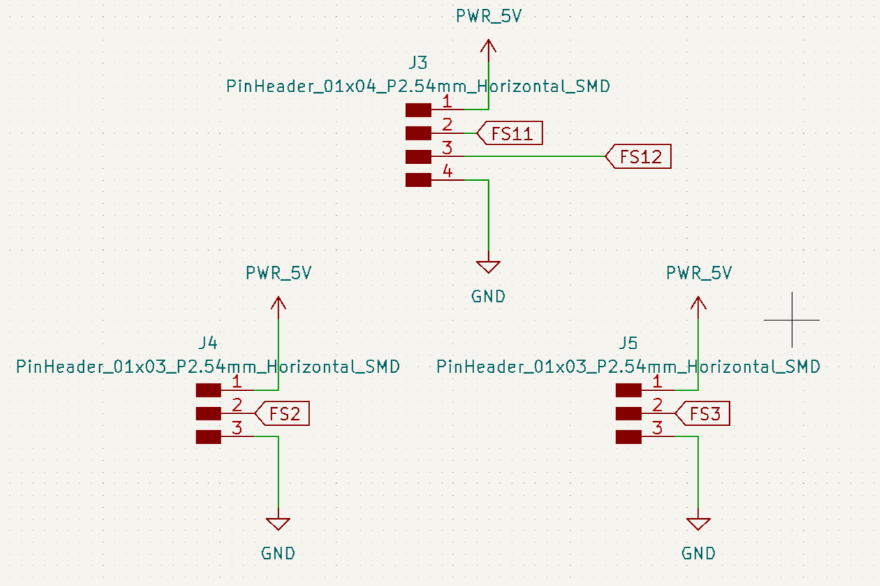
To make the board reusable for other sensors later, I broke out a few more spare GPIO pins to additional pin headers, labeled FS2, FS3, FS11, and FS12 (FS standing for Free Sensor) — each with its own 5V and GND.
Final Schematic
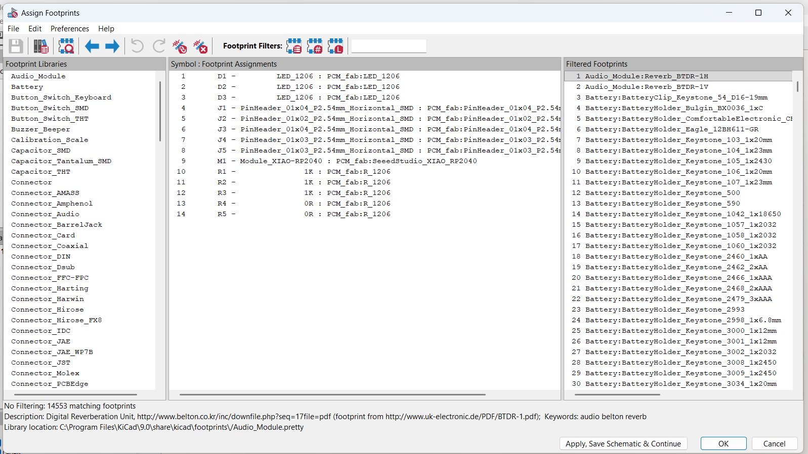
Once all the components were placed and connected — using both direct wires and global labels for the power rails — I went to Tools > Assign Footprints to double check that every component had a footprint set. Without this, KiCad won’t let you generate the PCB layout properly.
ERC — Electrical Rules Check
Before moving to PCB layout, I ran the Electrical Rules Checker (Inspect > Electrical Rules Checker).
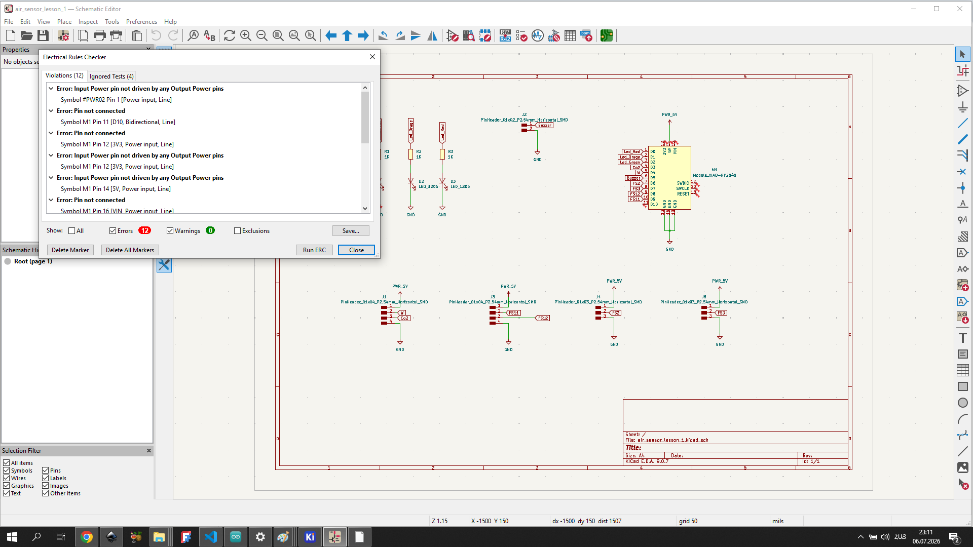
The ERC reported 12 errors — mostly “Pin not connected” warnings for unused pins on the XIAO RP2040 (3V3, 5V, VBUS, and a few GPIO pins that I intentionally left unconnected since they’re not used in this design) and “Input Power pin not driven” errors for the same power pins. These are expected for a board where not every microcontroller pin is used, and they don’t affect the board’s functionality.
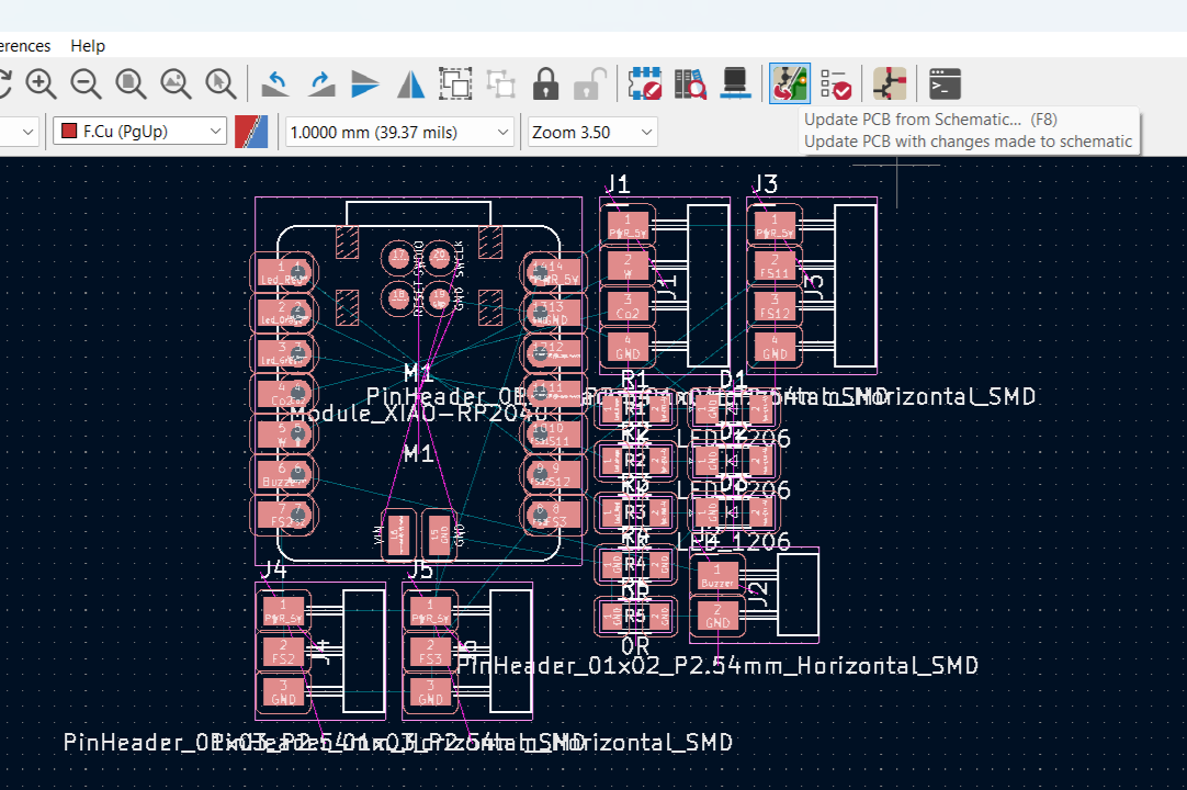
PCB Design
With the schematic complete, I switched to the PCB Editor and used Update PCB from Schematic (F8) to bring all my components into the PCB view.
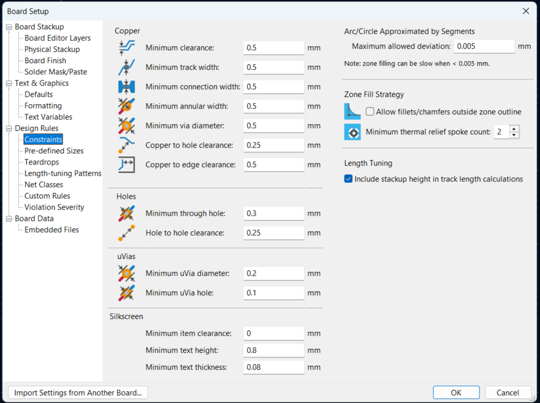
Before placing anything, I set up the Design Rules (Edit board setup → Design Rules → Constraints) — minimum clearance and minimum track width — based on the 1/64 inch end mill we use for PCB milling at the lab.
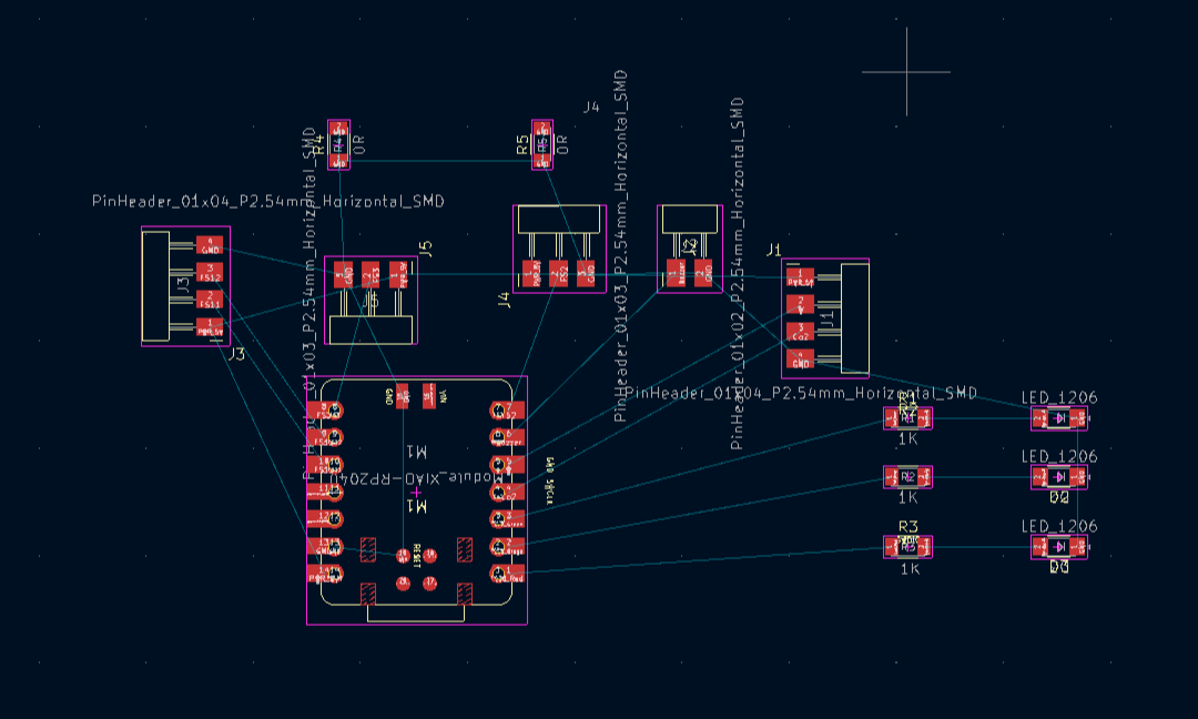
I then arranged the components on the board: the XIAO RP2040 in the middle, the pin headers around the edges close to where their wires would need to exit, and the three LEDs with their resistors lined up together on one side for a clean look.
Routing and the GND Zone
I routed the signal traces between the components:
and then used the Add Filled Zone tool to flood the rest of the board with a GND copper zone. This is where I ran into the trace-crossing problem mentioned earlier, solved with the two 0 Ohm bridge resistors.
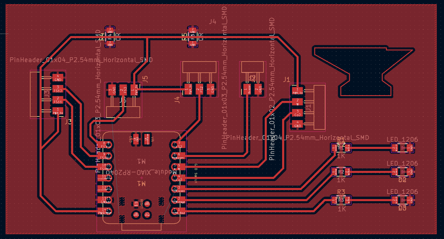
Mounting Holes and Board Outline
I added four mounting holes near the corners of the board for screws, and drew the board outline on the Edge.Cuts layer, which is the layer the milling machine uses to know where to cut the final contour of the board.
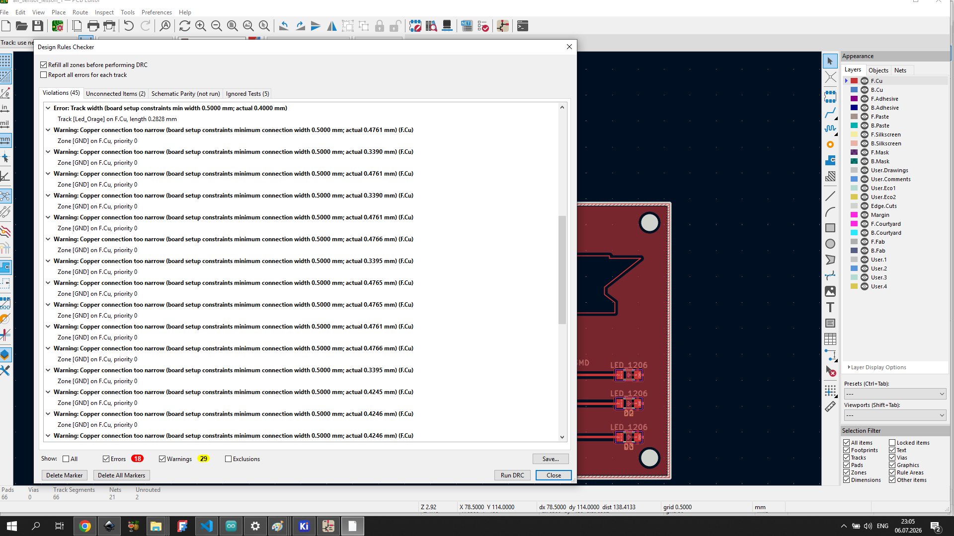
Design Rules Checker
Before considering the board finished, I ran the Design Rules Checker (DRC) to make sure the layout was actually ready for milling.
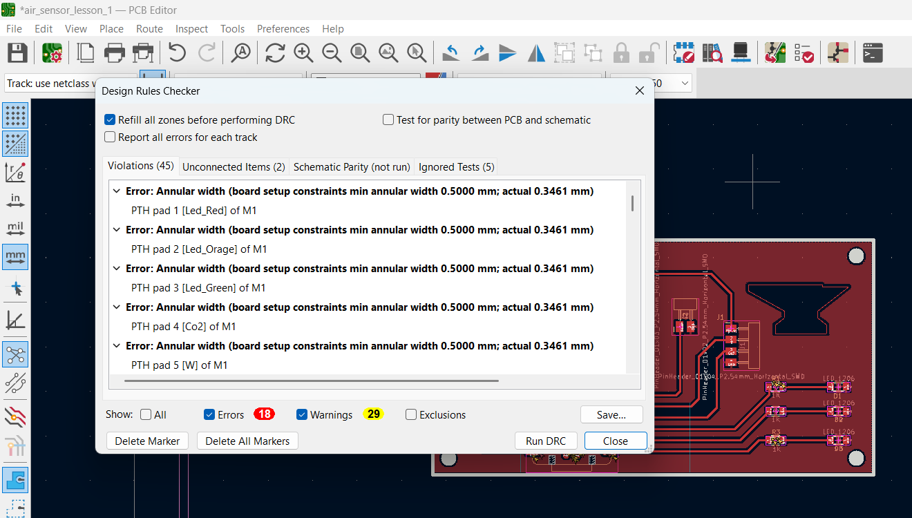
Most of the errors I got were related to clearance and track width violations — traces that were too close together or too thin for the values I had set earlier in the Design Rules. Such moments could not in any way affect the functionality of my board.
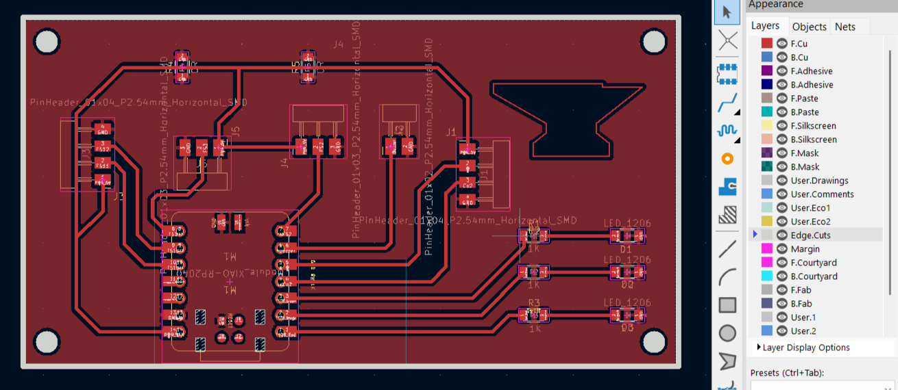
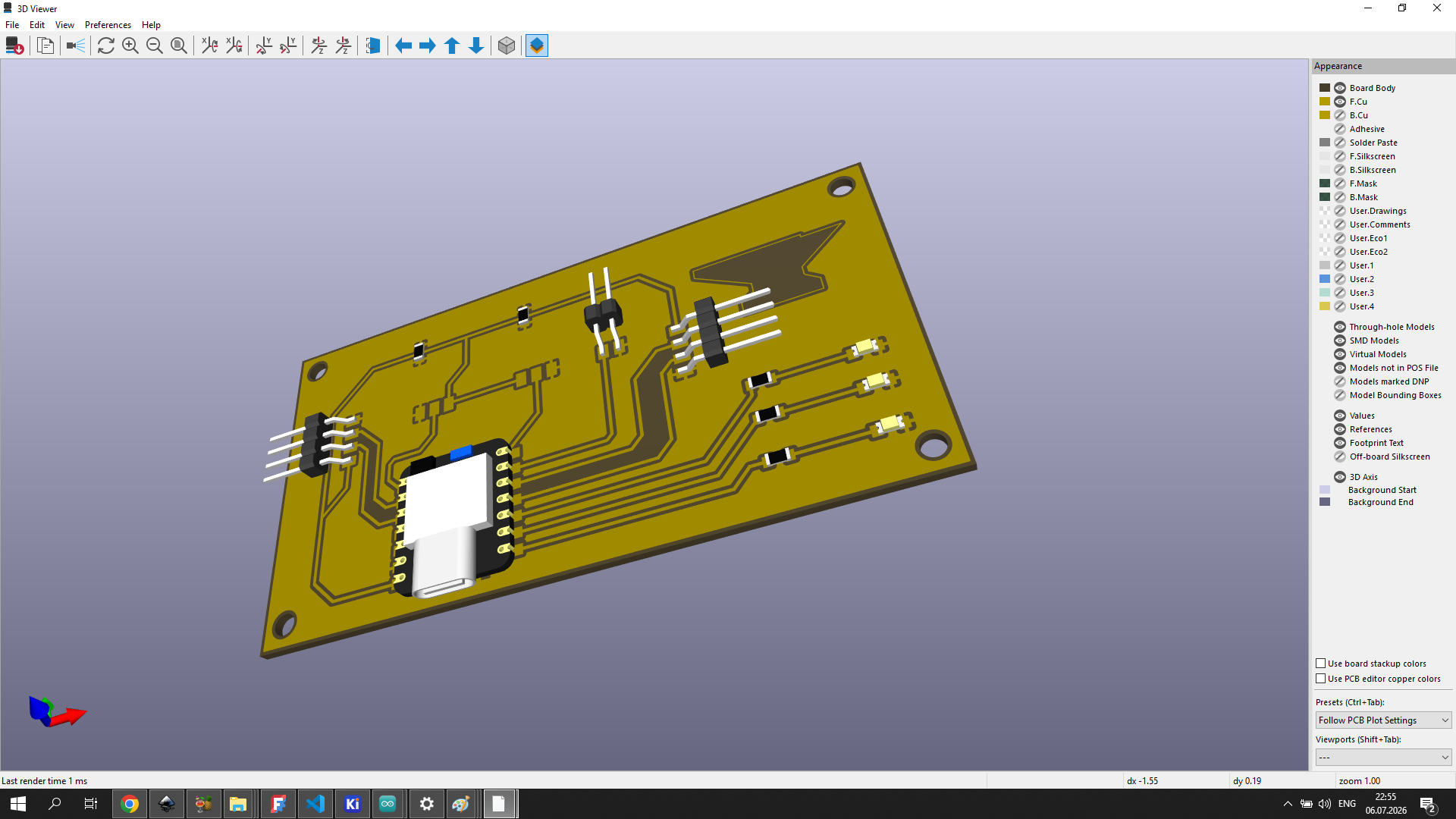
3D View
KiCad includes a built-in 3D viewer (View > 3D Viewer) that shows a photorealistic render of the board with all components in place. This was useful for a final visual check before sending the design to the milling machine.
Conclusion
This week I learned how to design a PCB completely from scratch. Working through the schematic forced me to think carefully about which signals needed power and ground, and the GND zone routing issue taught me a practical trick (0 Ohm bridge resistors) that I hadn’t seen before.