Week 08. Electronics Production
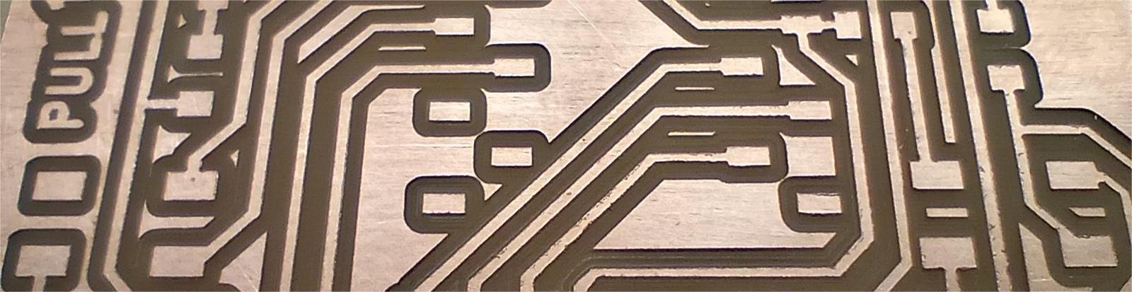
Table of Contents
- WEEKLY PLAN
- GROUP ASSIGNMENT: DESIGN RULES FOR PCB PRODUCTION
- INDIVIDUAL ASSIGNMENT: MAKE AND TEST A MICROCONTROLLER DEVELOPMENT BOARD
- USEFUL LINKS AND RESOURCES
- FILES
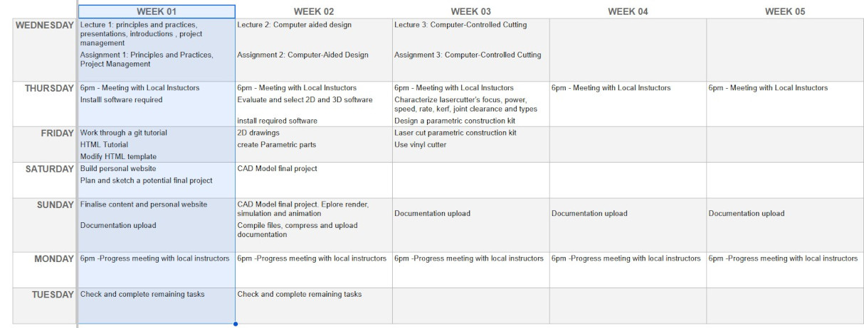
WEEKLY PLAN
Group assignment:
- Characterize the design rules for your in-house PCB production process
- Submit a PCB design to a board house
Individual assignment:
- Make and test a microcontroller development board that you designed
- Extra credit: make it with another process
GROUP ASSIGNMENT: DESIGN RULES FOR PCB PRODUCTION
This is the link to the Fab Lab León Group Assignments page. Since I am completing the group assignment on my own I left the documentation on this page.
WORKFLOW FOR ROLAND MODELA MDX-20A
I used to fabricate printed circuit boards (PCBs) using a UV light and an etching tank. This process involved working with chemicals and once the PCB was etched, I would drill holes for the components. This week, I am looking forward to learning about a different PCB fabrication process.
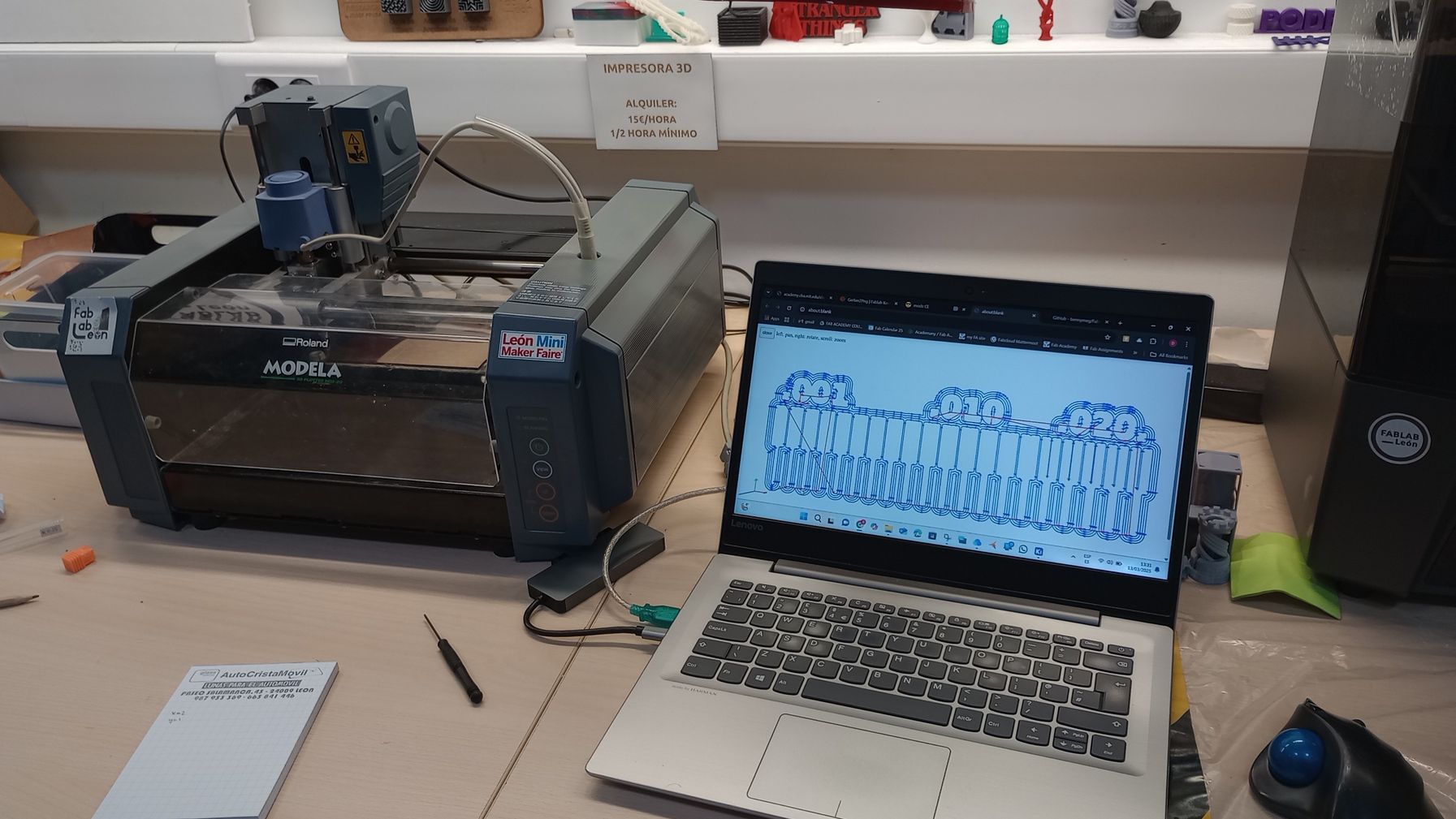
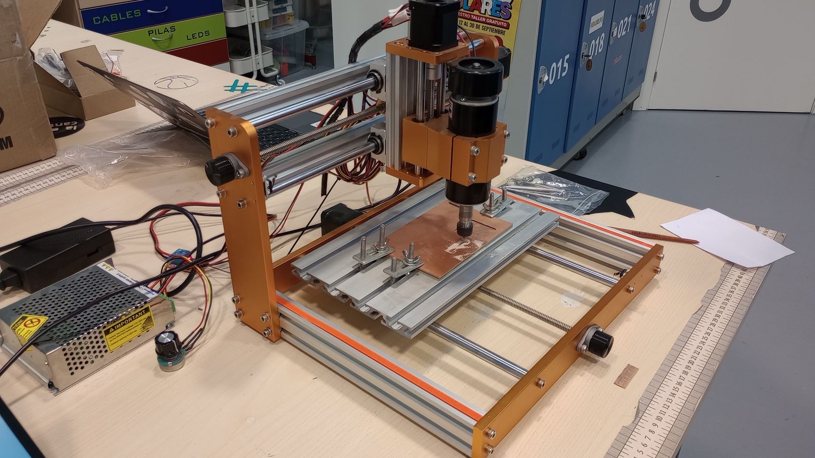
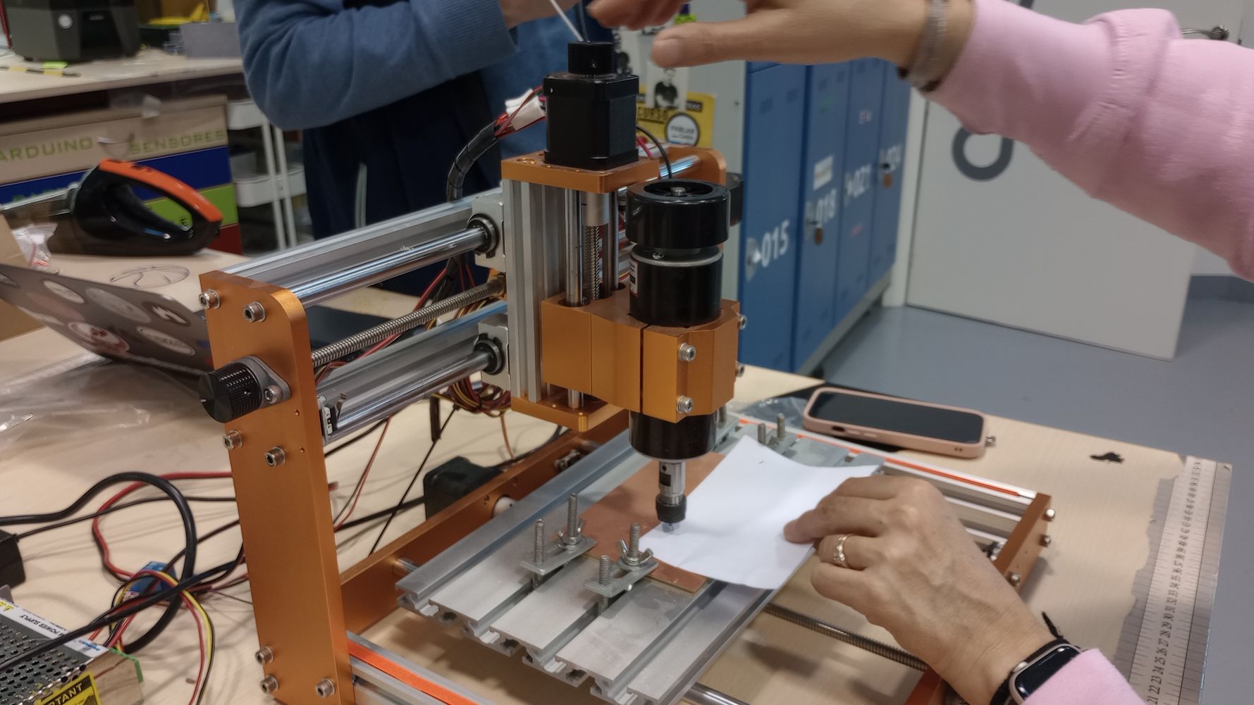
I spent two days at Fab Lab León, where I had the opportunity to use their CNC milling machine and learn about the production workflow they employ.
I started using their Roland Modela MDX-20A.
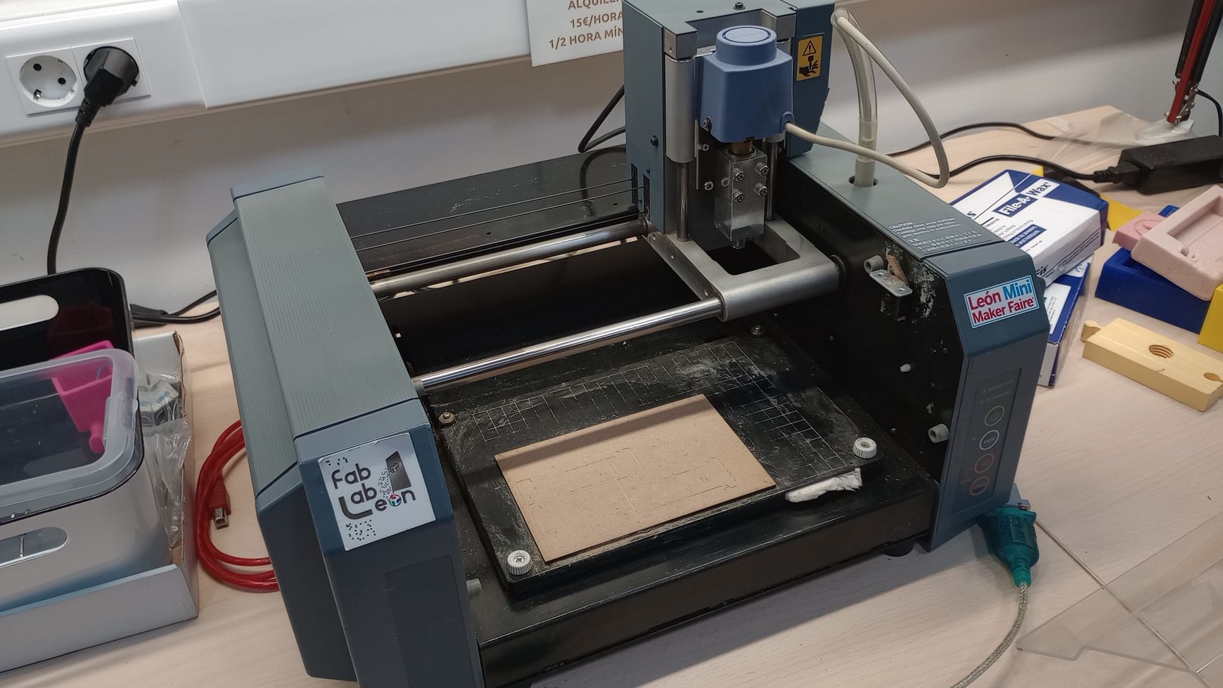
| Model | Roland MDX-20A |
| Working area | 203.2 mm (X) x 152.4 mm (Y) x 60.5 mm (Z) |
| Feed rate | 0.1 to 15 mm/sec |
| Spindle | 6500 rpm |
| Tool chuck | 1/8 in. or 6 mm tool chuck |
| Acceptable materials | Wood, Plaster, Resin (modeling wax, Styrofoam), wood, Aluminum (A5052 according to JIS), Brass |
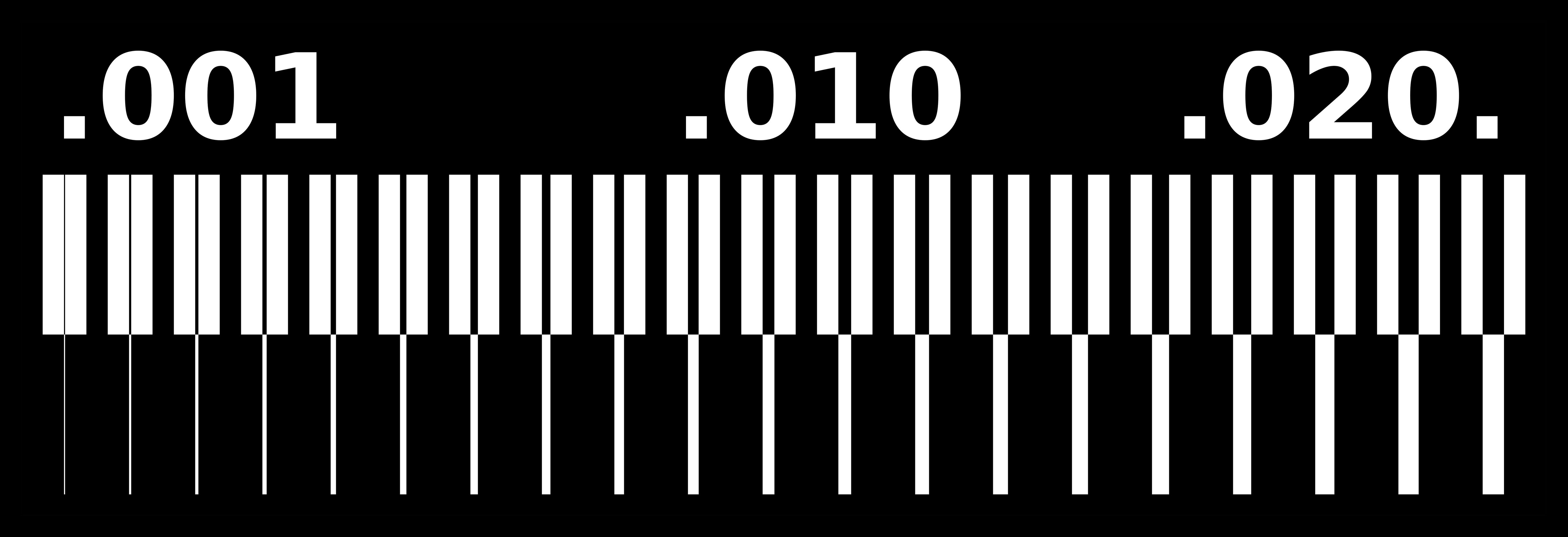
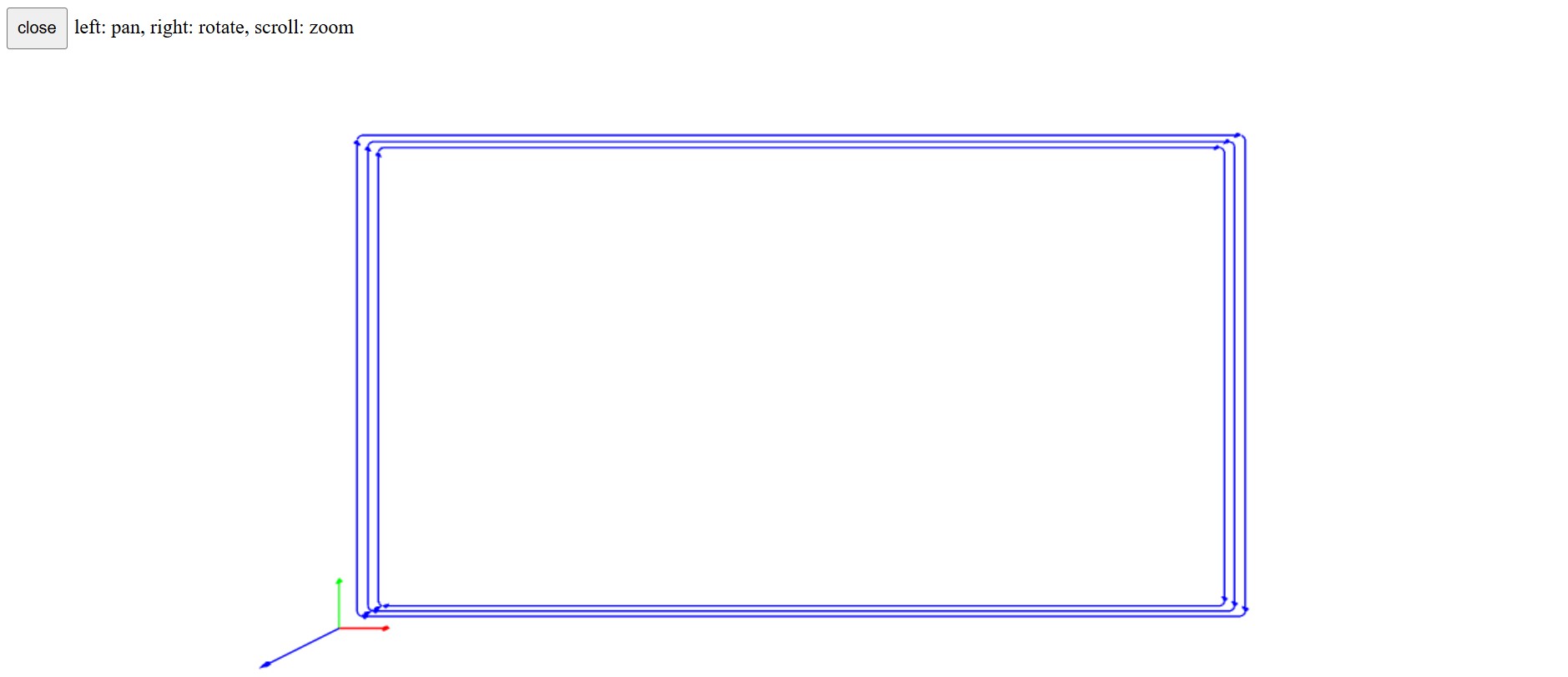
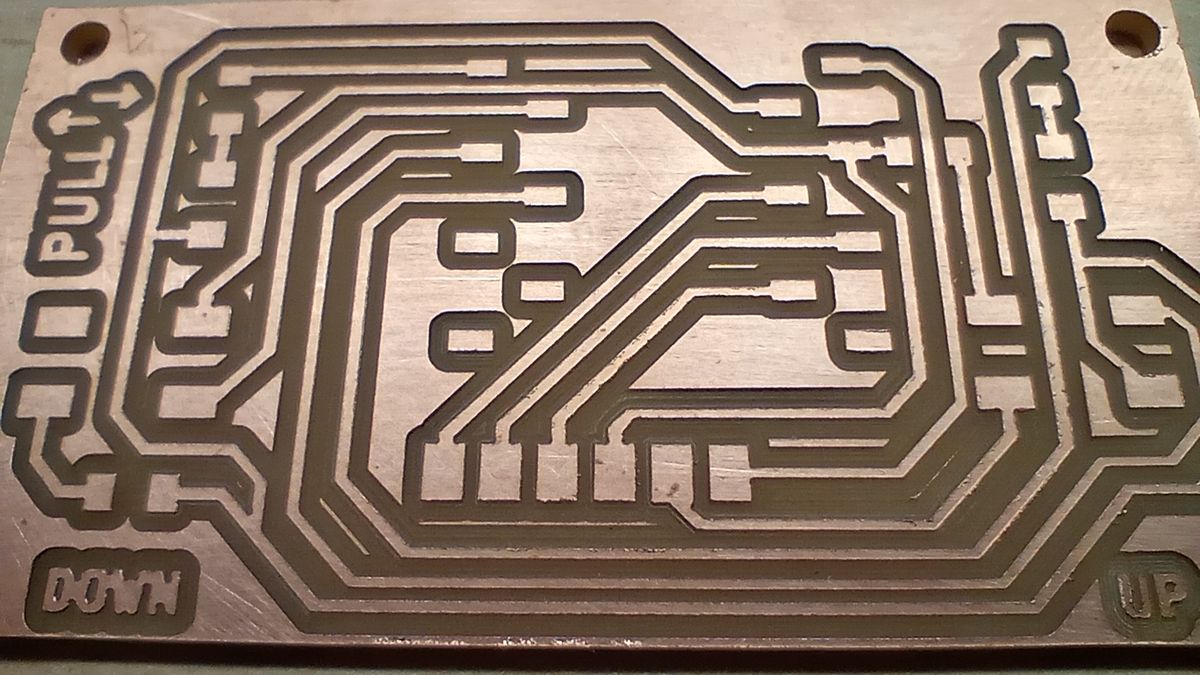
The following steps show the workflow process to cut the line test provided by Fab Academy, which involves preparing the file, selecting the toolpath strategies and setting up the machine.
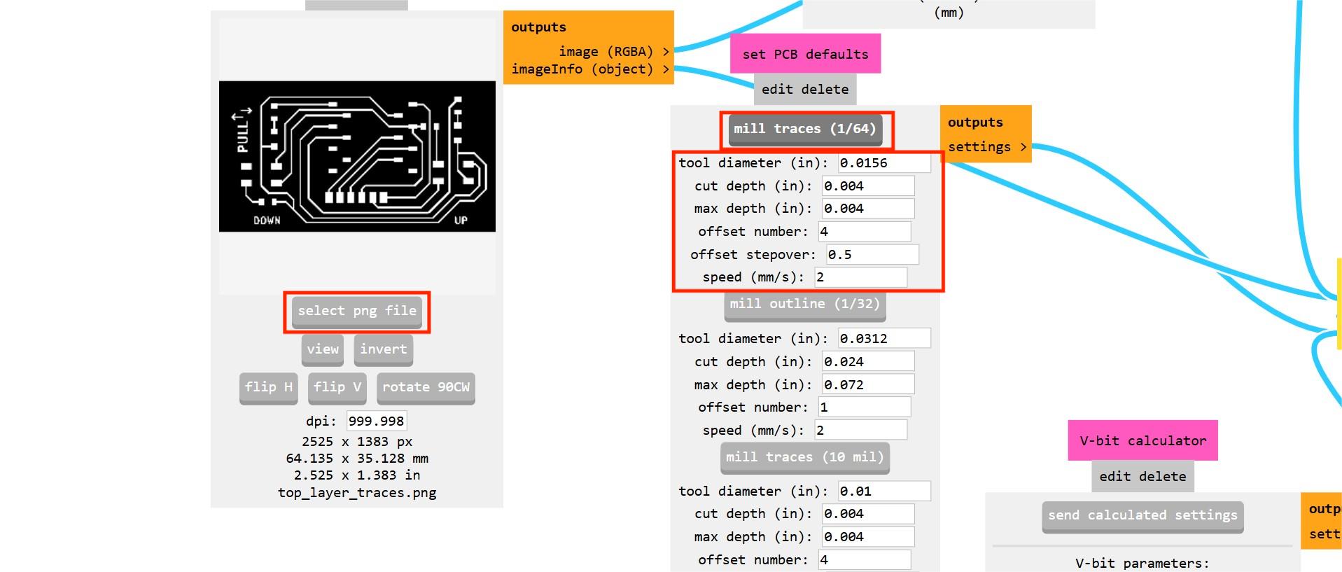
I start by downloading the png files for the traces and exterior edge.
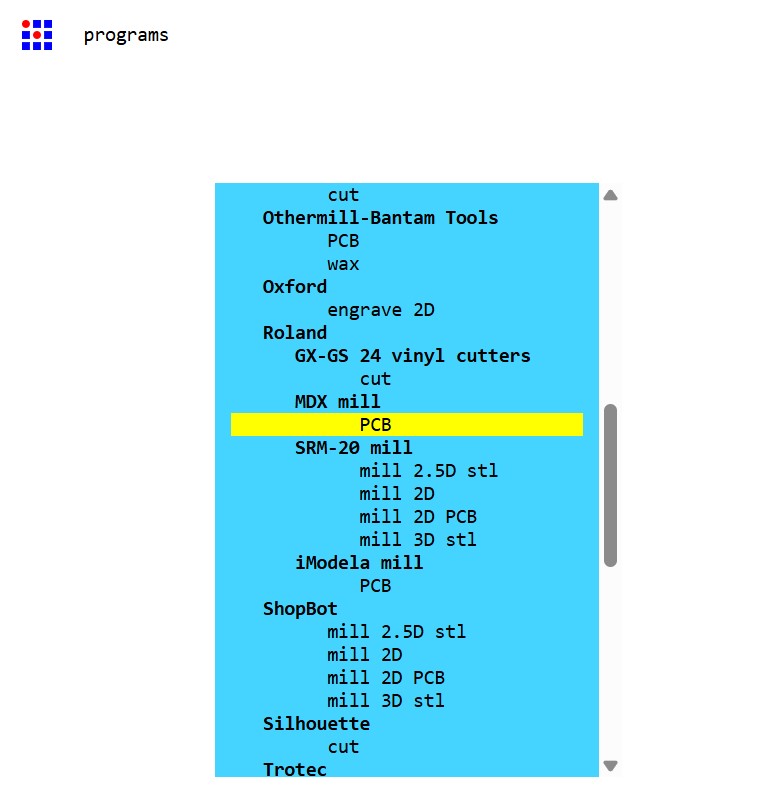
I open Mods>programs>open program and select Roland MDX mill PCB.
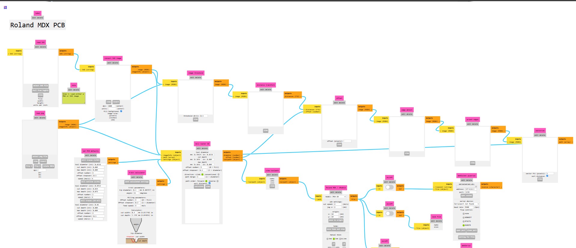
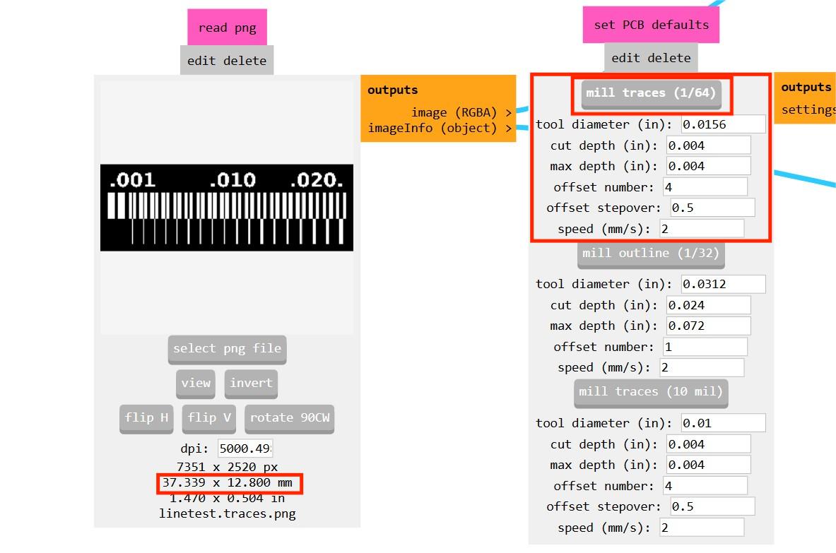
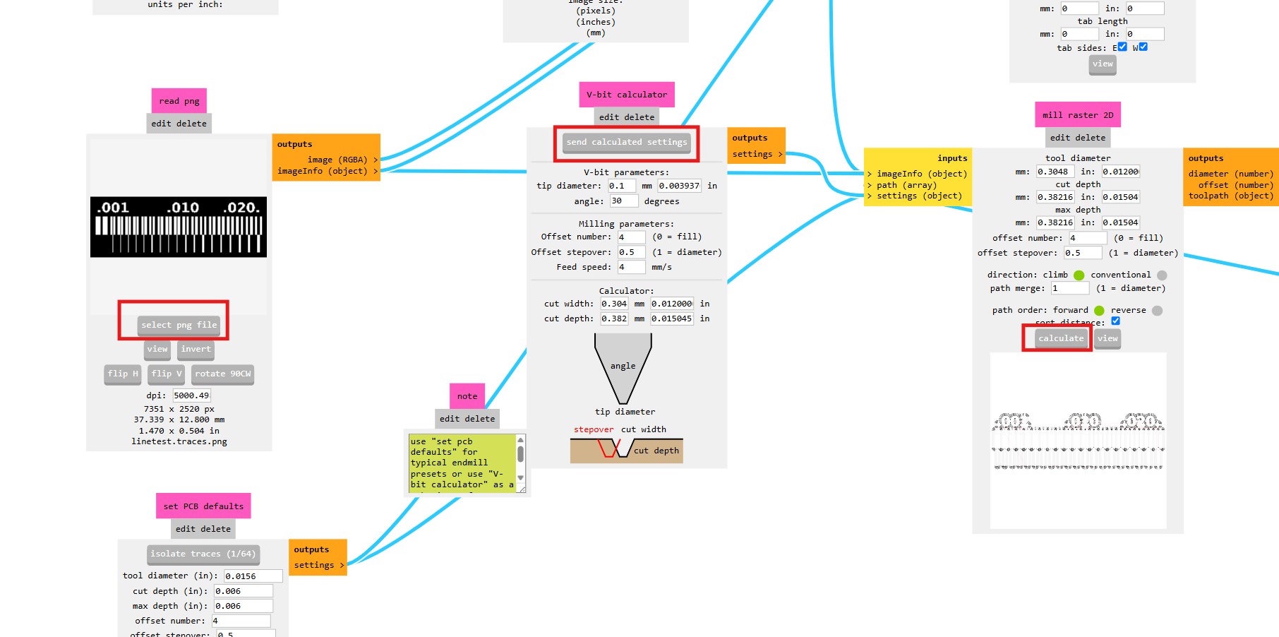
I load the traces png file and select the mill traces (1/64). This selects the milling strategy for traces, with a cut depth of 0.004in (0.10 mm), 4 passes around the traces, with a stepover of 0.5 times the tool diameter. Following Adrian’s recommendation I reduced the speed (feed rate) from 4 to 2 mm/s.
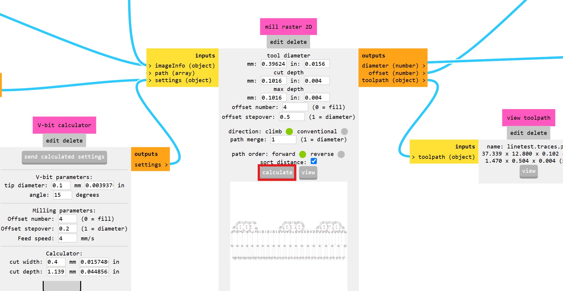
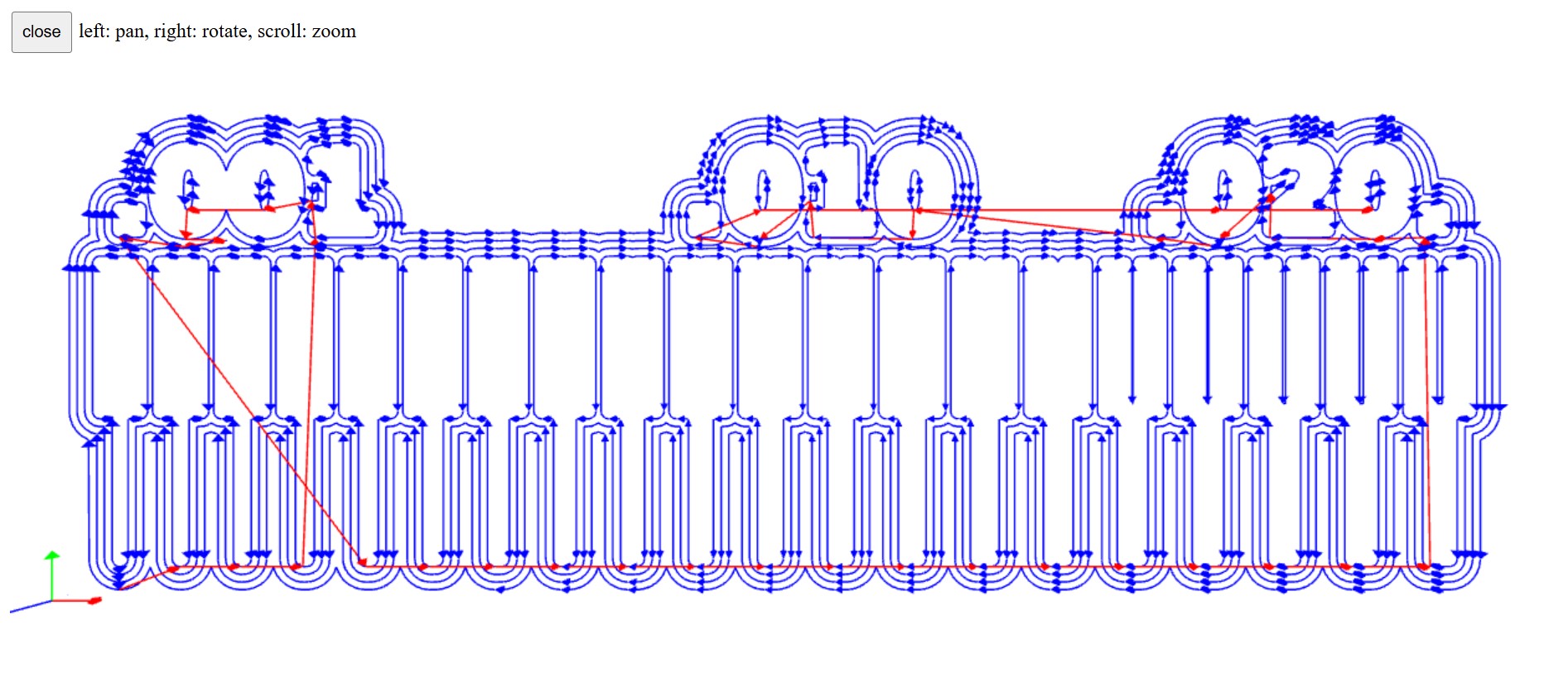
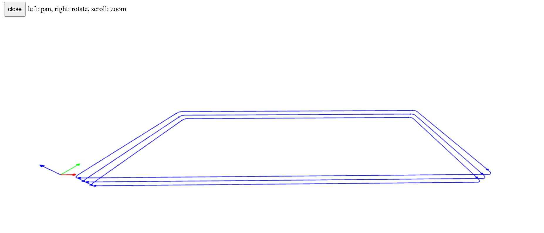
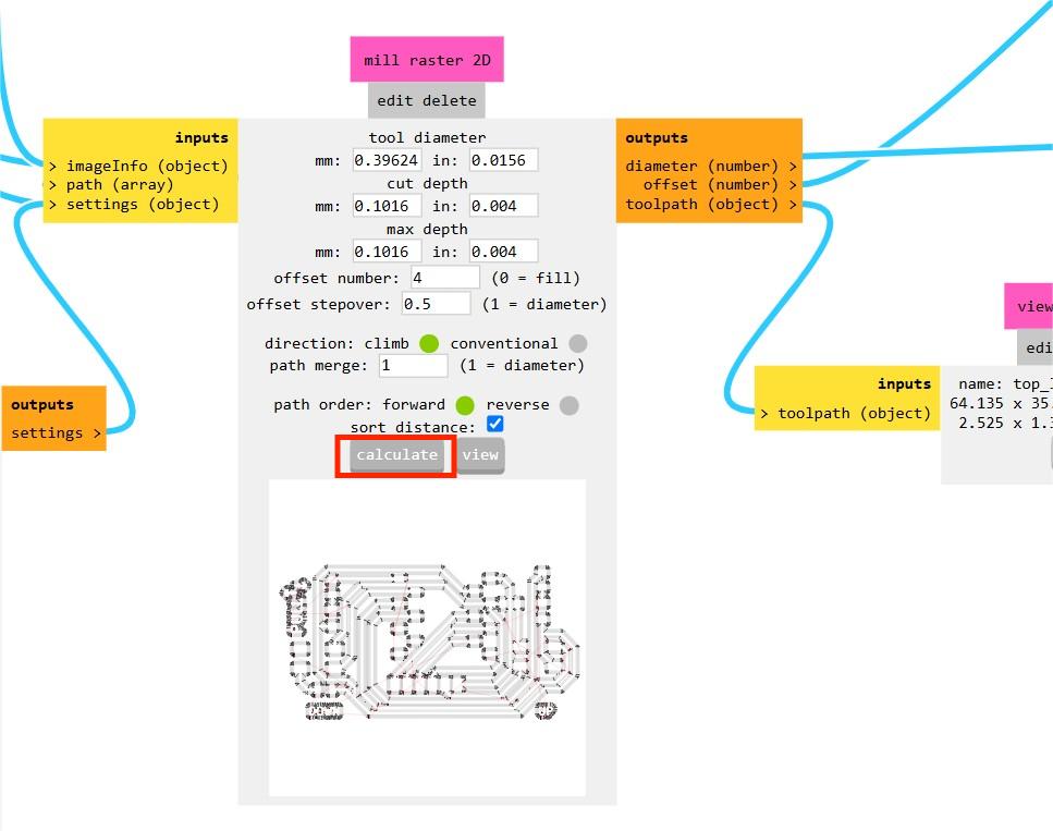
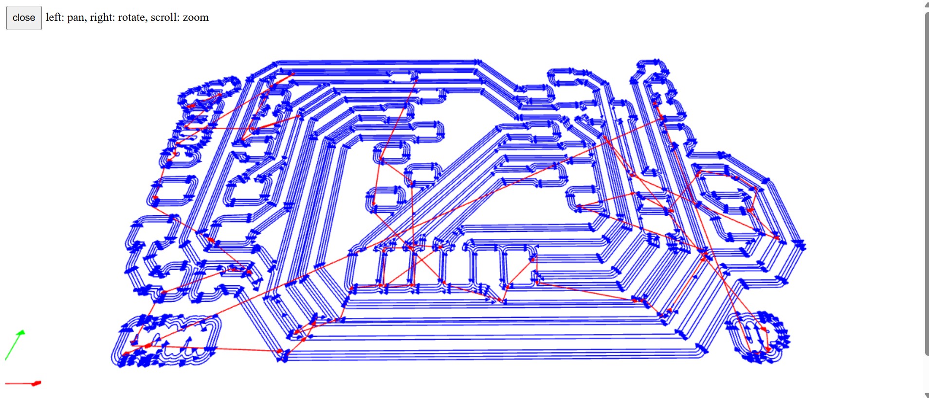
A new tab opens showing the generated toolpaths. The software uses the W&B image to generate toolpaths that will remove the material around the white traces and numbers.
CONNECTING TO THE ROLAND MDX-20A
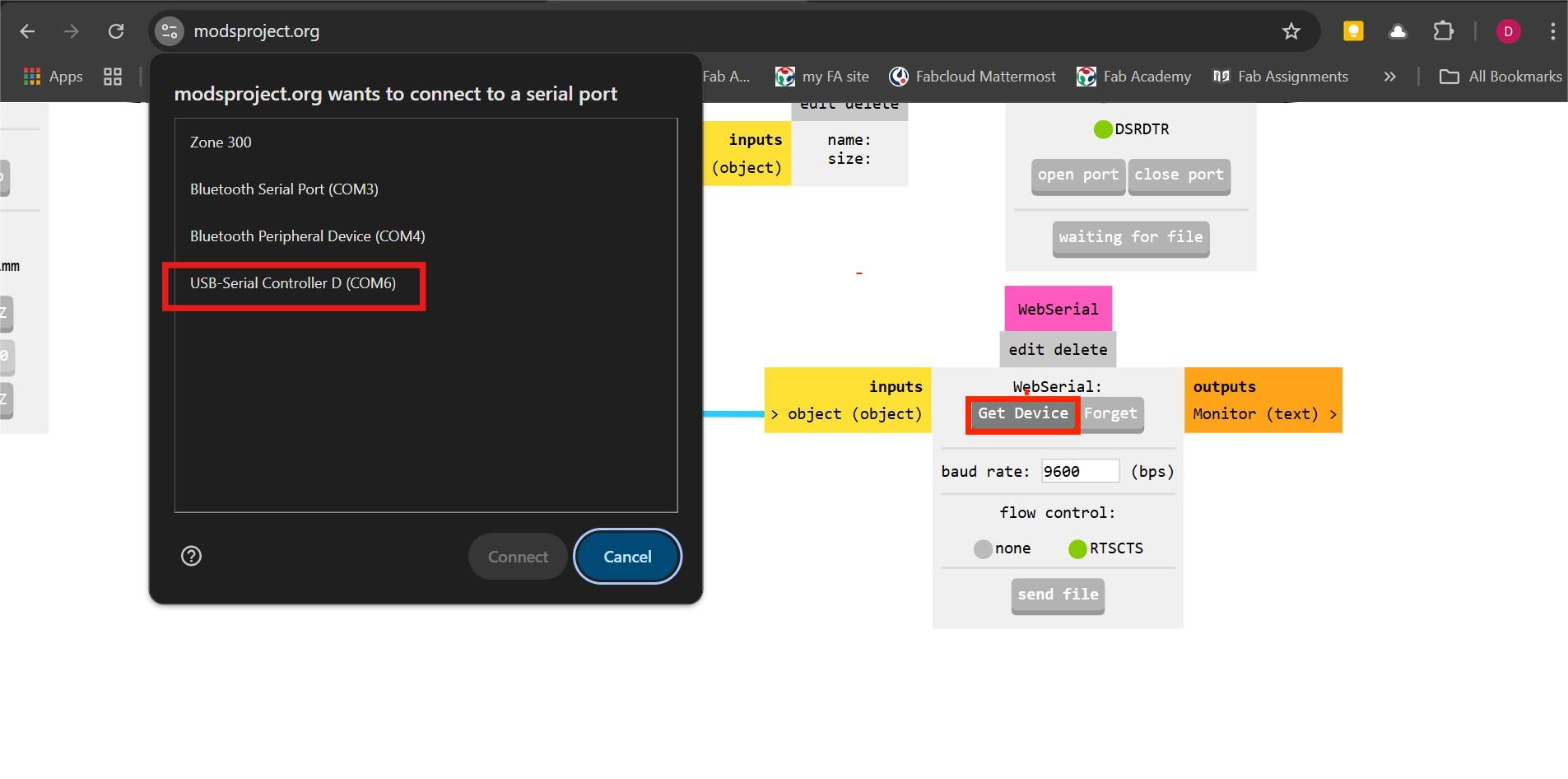
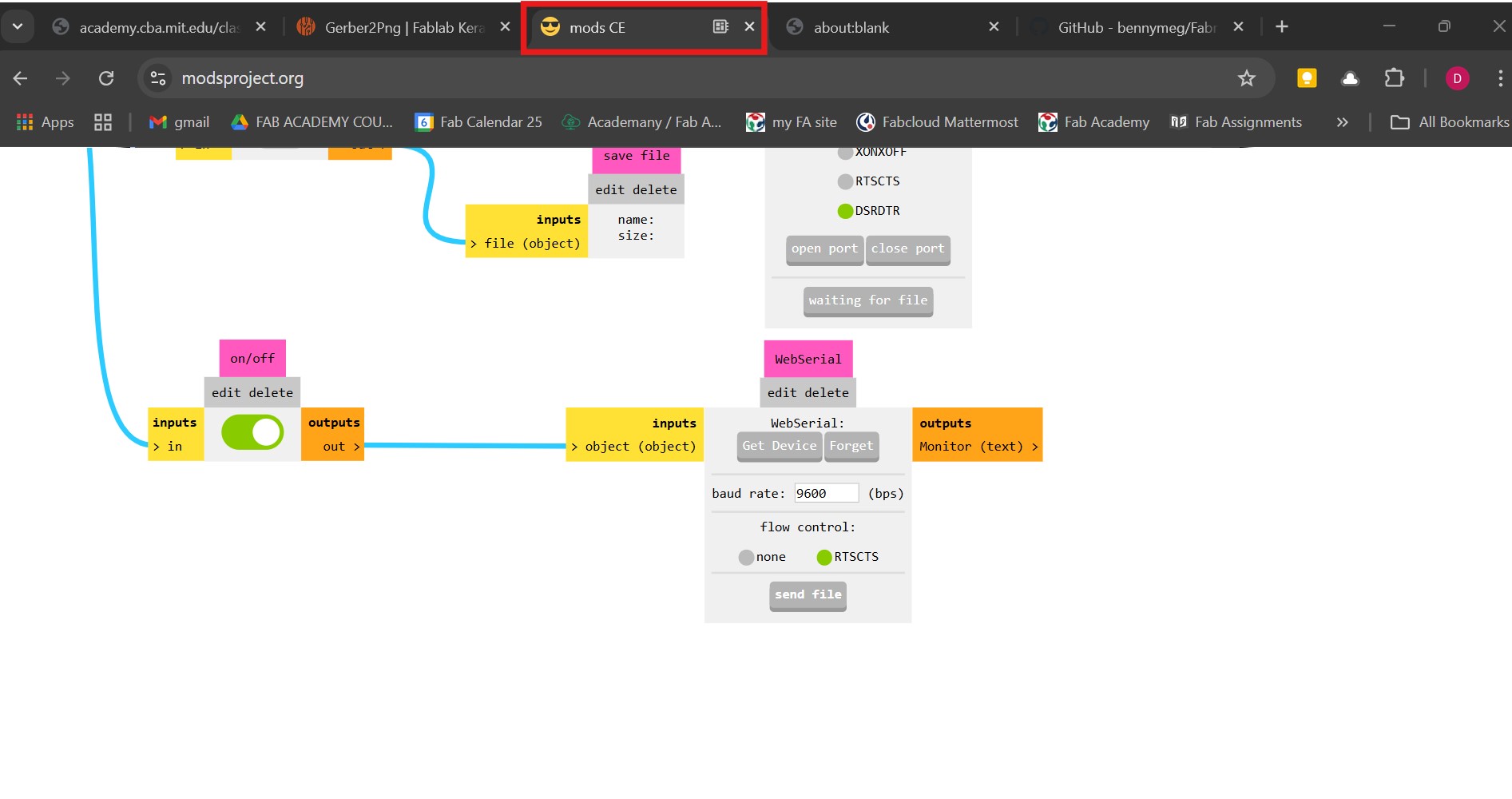
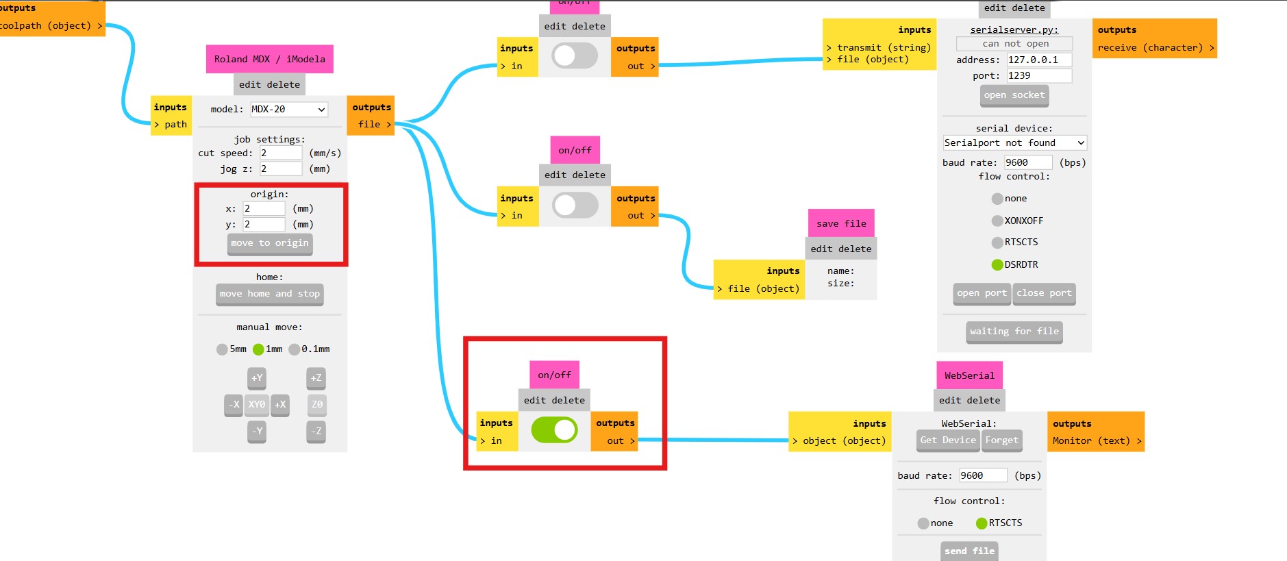
With the laptop connected to the machine via USB I go to Mods>Webserial and click on Get Device. I select the USB serial port. When the machine is connected a small icon appears on the browser tab.
SETTING UP THE CNC MILLING MACHINE
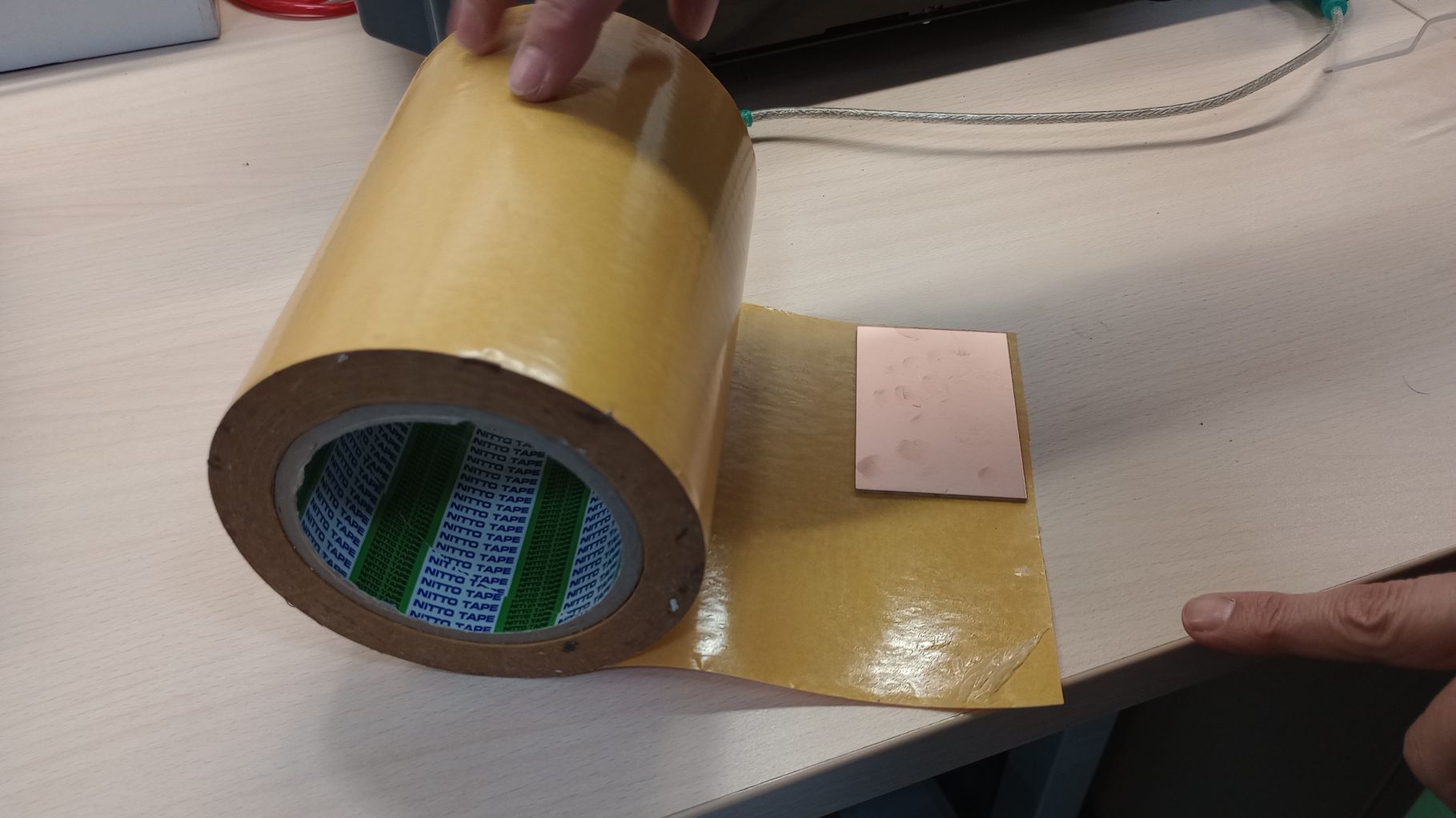
Now I proceed to set up the machine. I stick double sided tape to the PCB blank so I can secure it on top of the MDF sheet used as sacrificial piece.
Material: FR-1 (phenolic paper) Printed Circuit Board 75 x 50 mm
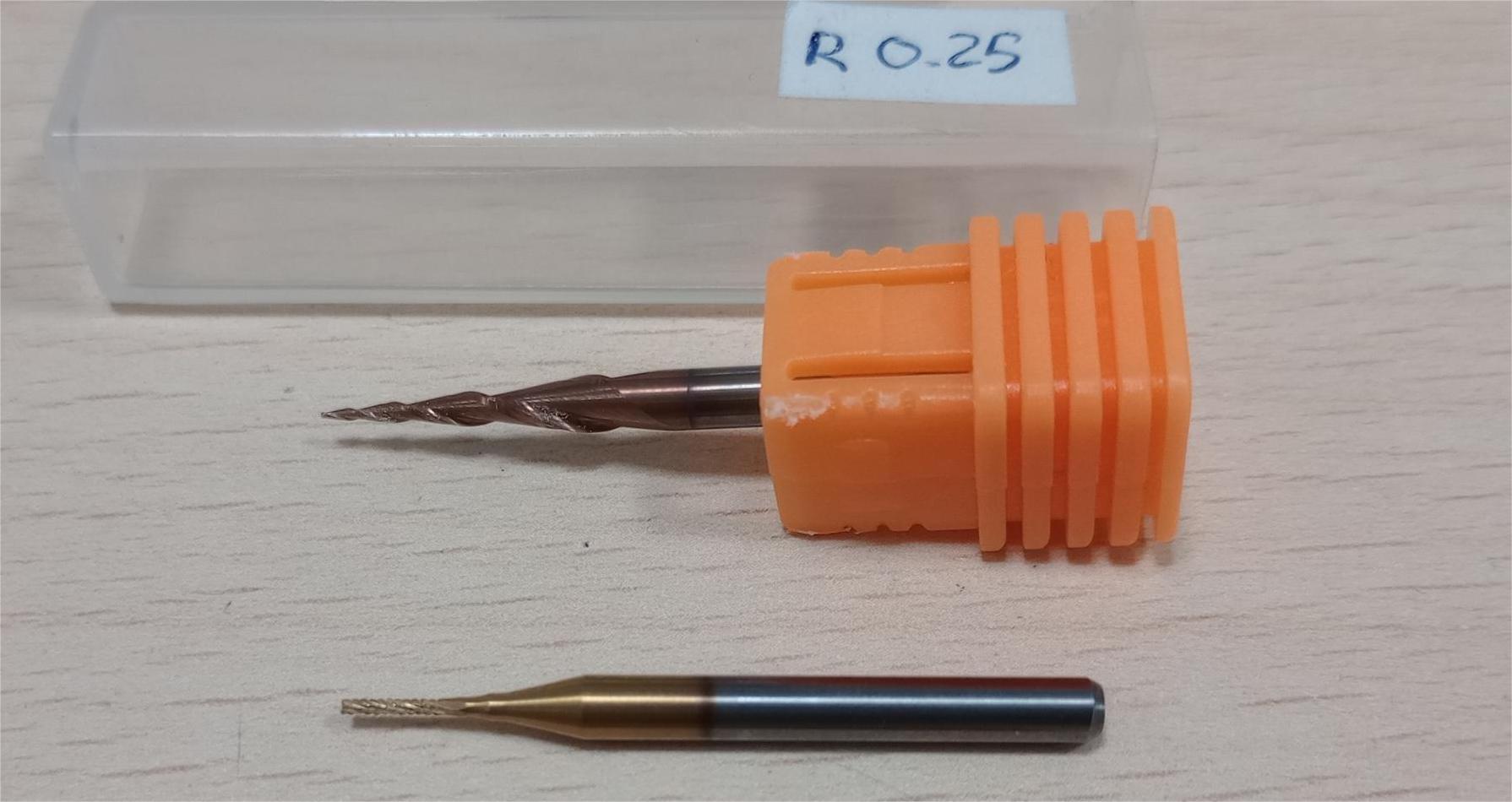
Fitting The End Mill And Setting Z0
To machine the traces: R0.25mm conical spiral ball nose bit
To cut the board edge: 1/32 in (0.8mm) end mill
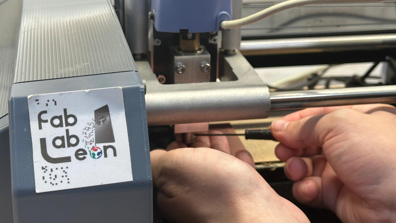
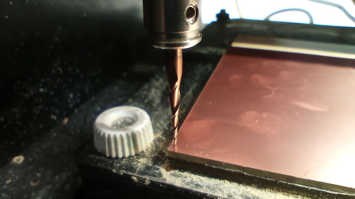
I start the machine without milling tools and let it move to the home position on the bottom left corner. I lift the carrier to have better access to chuck. With one hand I carefully place the cutting tool in the chuck and tighten one of the screws enough to hold the bit.
Using the TOOL DOWN button on the device I lower the carriage until the tip of the cutting tool is a few mm above the PCB surface. Then, I loosen the screw, let the bit touch the surface and now I tighten both screws. I take care not to over doing it to avoid damaging the threads on the chuck.
Setting XY origin
The home position is set up on the bottom left corner of the board. To avoid cutting right in the corner I set up the origin in Mods as X=2mm Y=2mm. I write it down just in case I loose the origin and I have to set it up again.
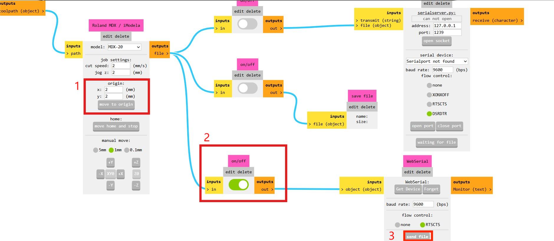
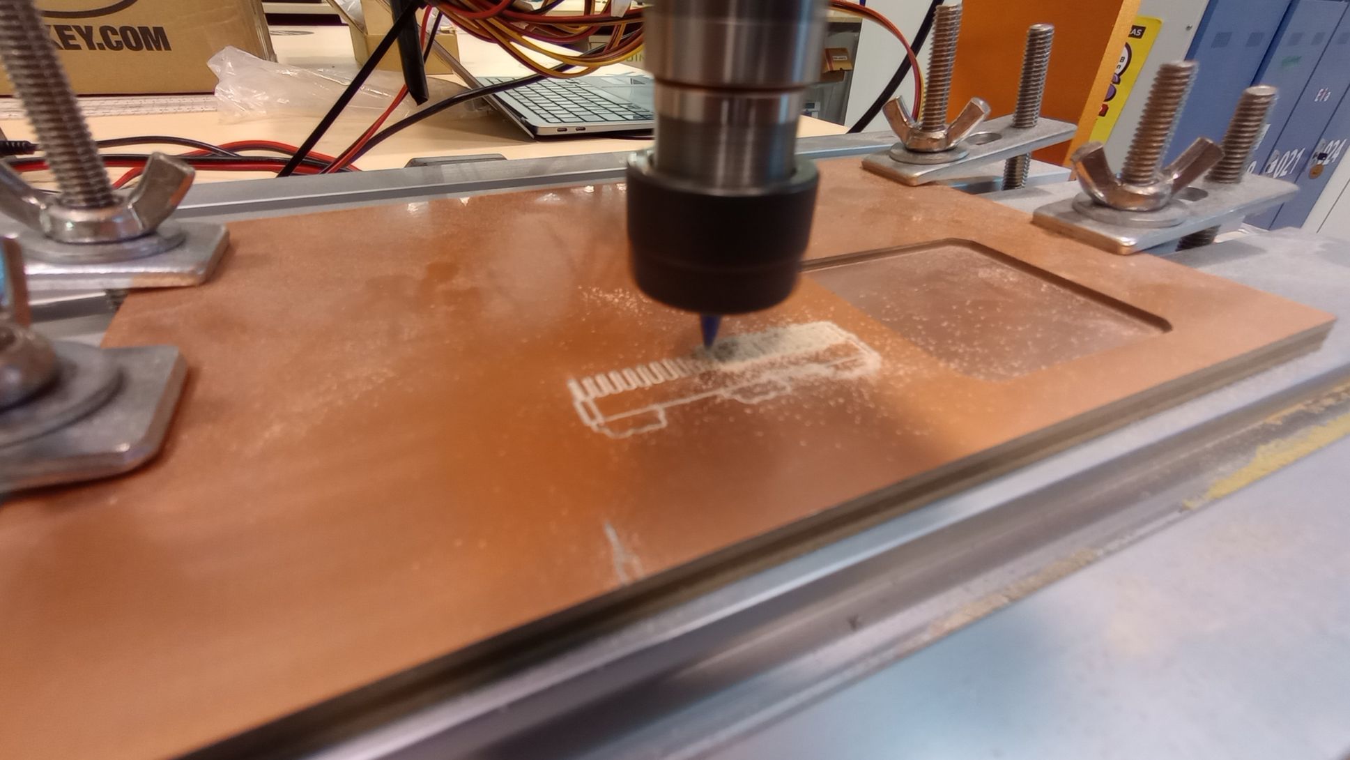
With the end mill fitted and the xyz origin for the job set up, I send the traces file to cut.
After the milling process finishes, I remove the end mill, I hoover the dust and I prepare the file to cut the edge.
Next, I load the interior png file in Mods and this I select the mill outline (1/32) strategy.
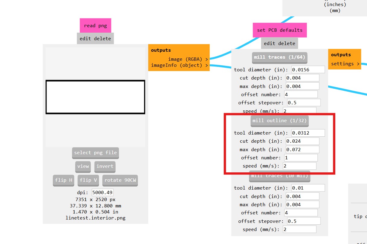
I click Calculate and toolpaths are generated. In this case 3 passes will cut through the thickness of the blank. As the blank is stuck with double sided tape there is no need for tabs.
I fit the 1/32 end mill on the milling machine repeating the process explained above to set up Z0. the XY origin values are the same as before.
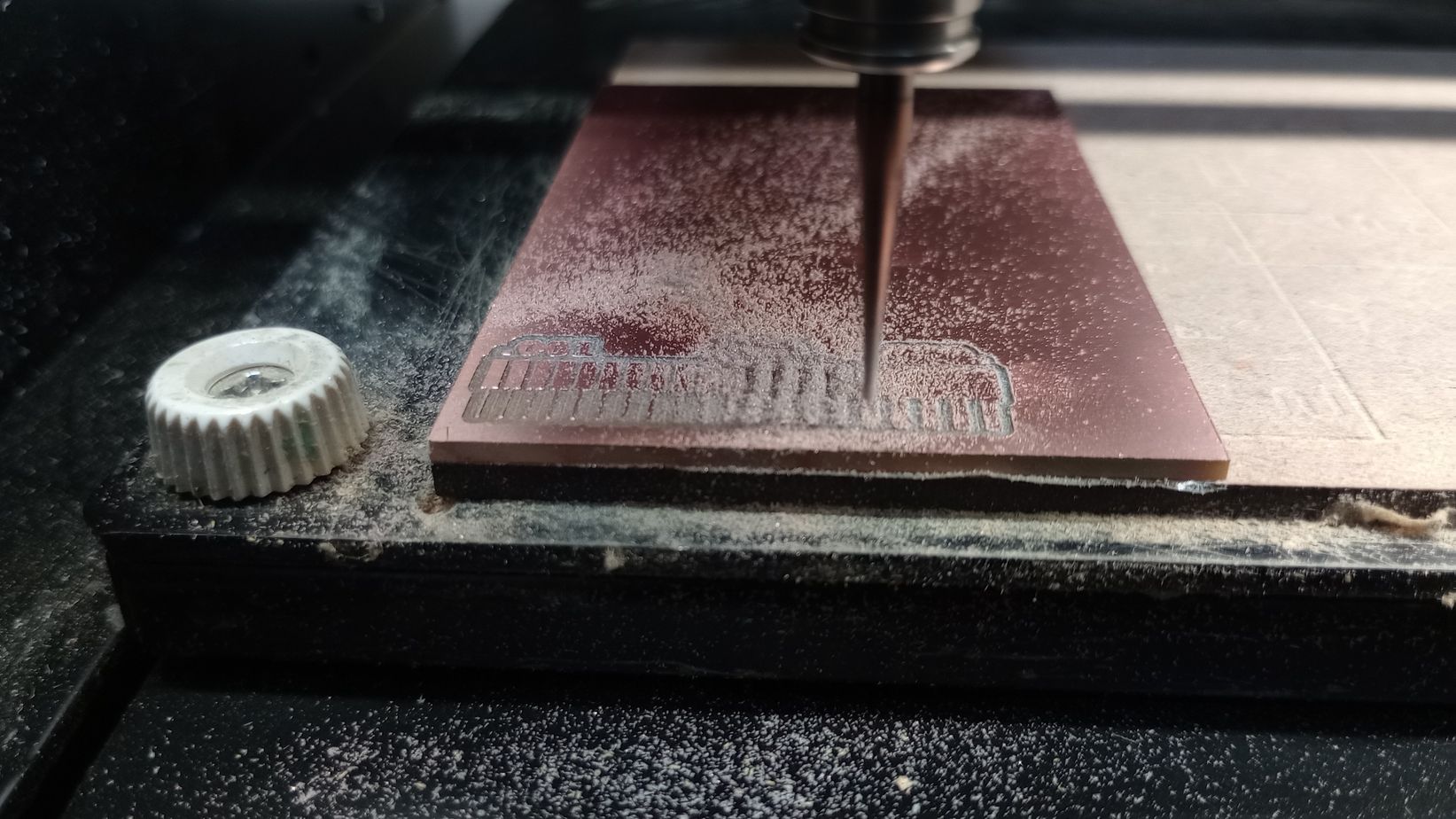
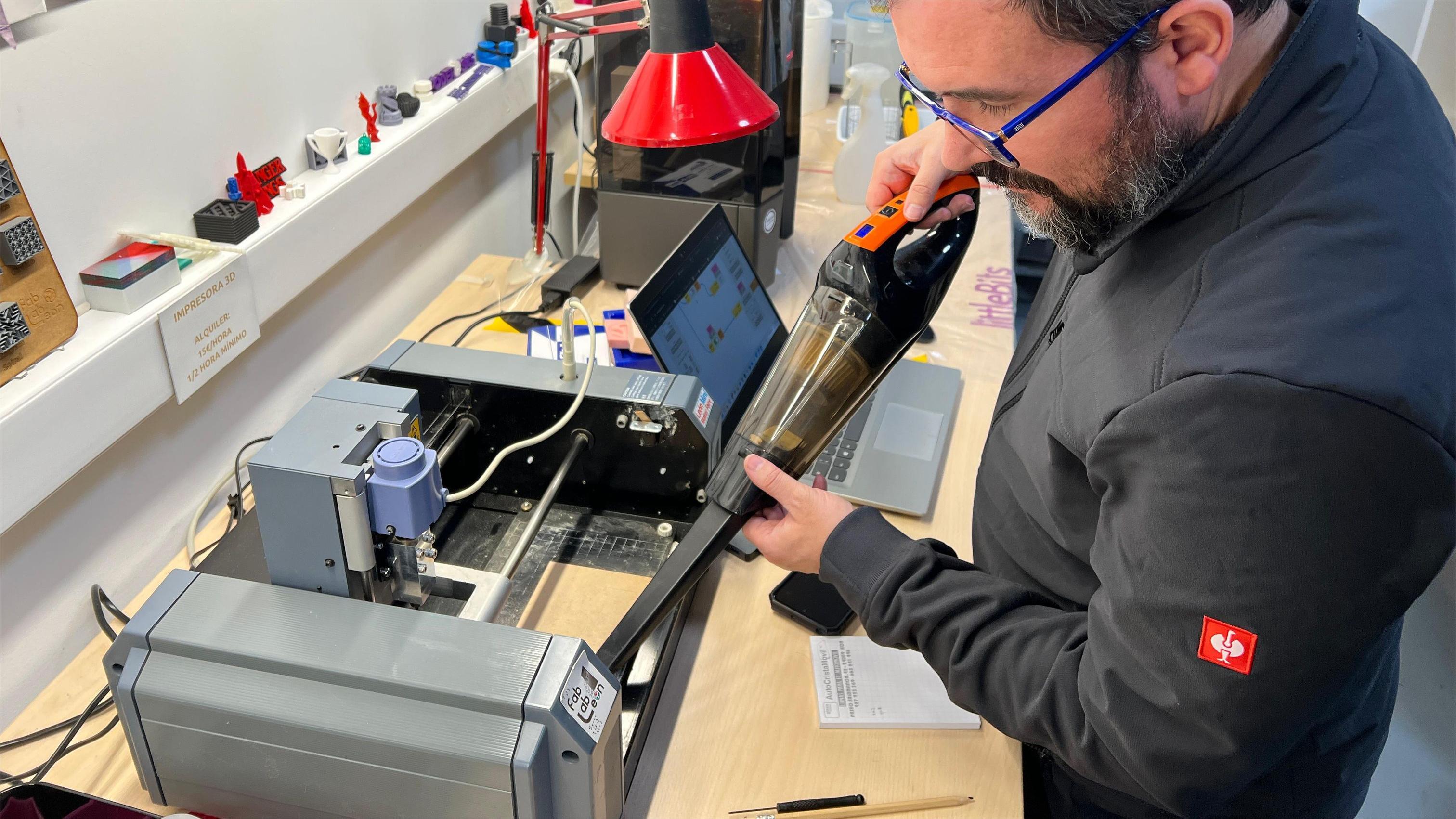
This time more dust is produced. As this type of machine does not have extraction I remove the dust with a handheld vacuum cleaner after each milling operation.
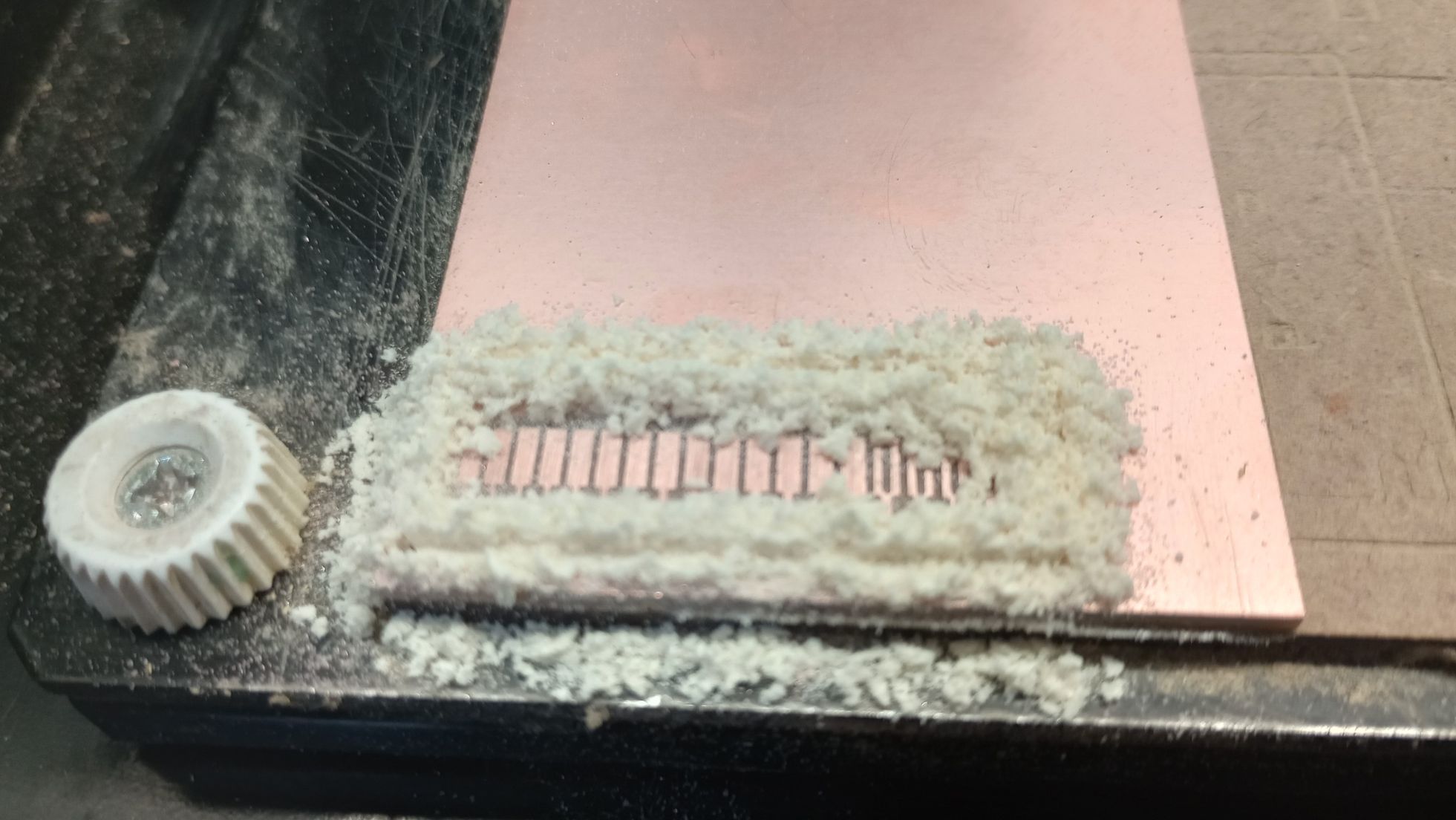
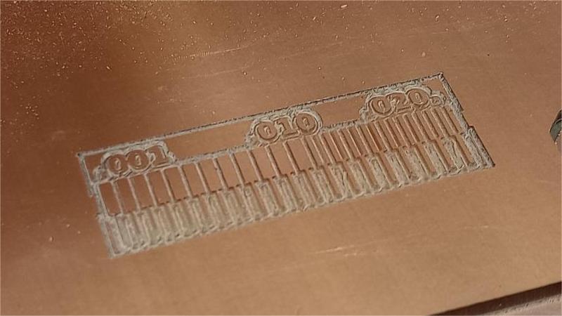
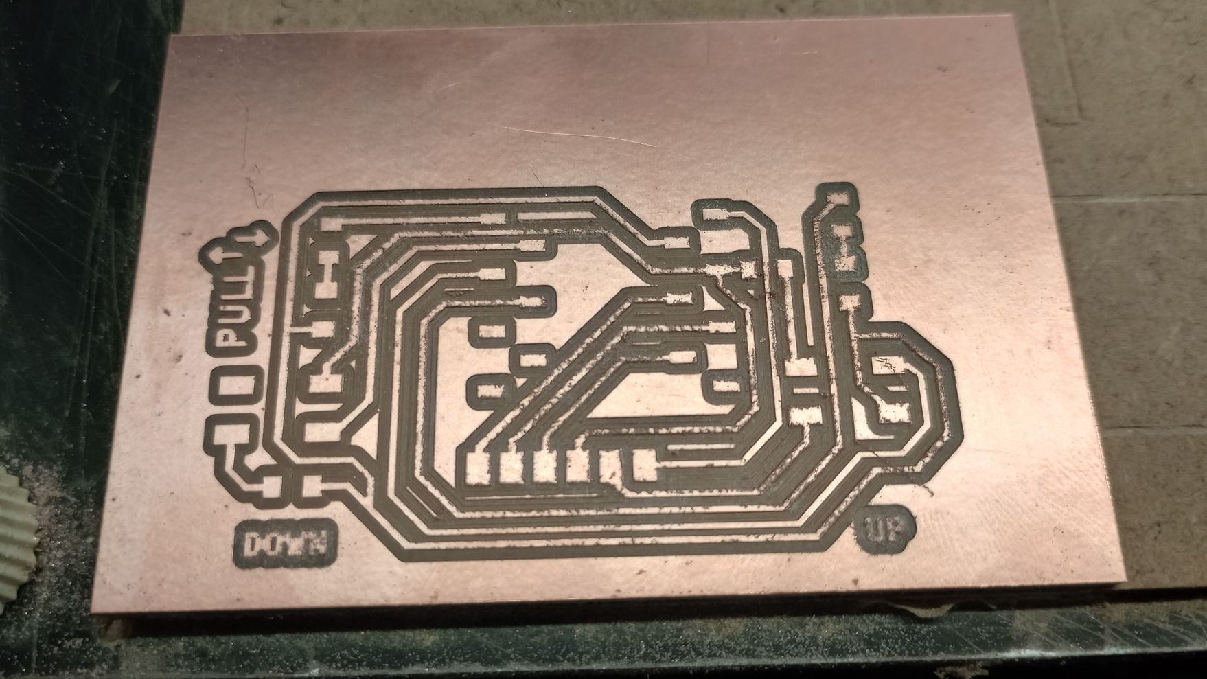
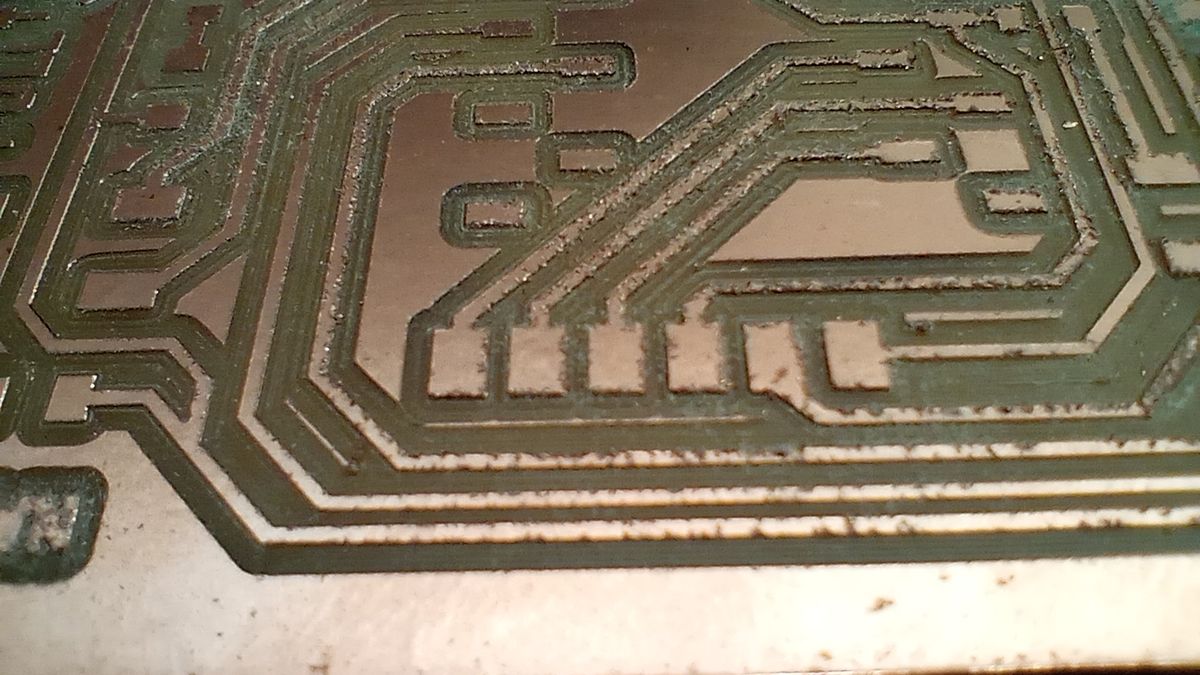
In the close-up photo, some copper burrs are visible on the edges of the test piece. It's important to handle the piece carefully, as the edges can easily cut your fingers. I use fine wire wool to clean, smooth, and remove any metal burrs
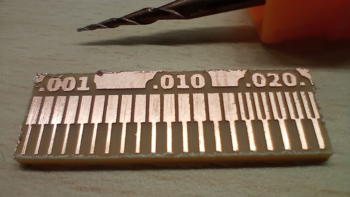
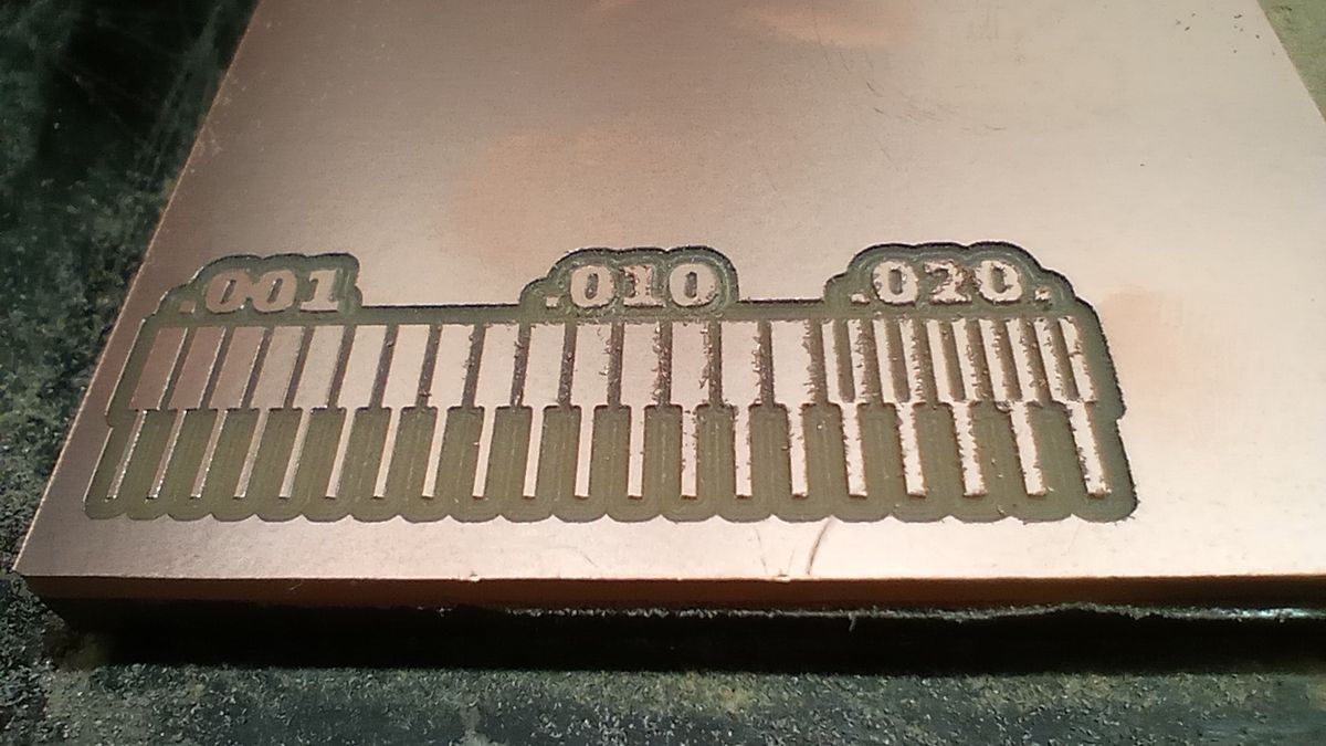
In this test, I observed that the conical ball nose tool used for milling the traces cannot cut more than five "between-tracks" lines on the upper part when the thickness is under 0.020. Additionally, I noticed that it failed to mill the finer tracks; the ones thinner than 0.001 all appear to be the same thickness, unlike what is shown in the PNG file.
However, this workflow and the milling tools can still be used for the individual assignment, where I will be fabricating the PCB board I designed during week 6.
WORKFLOW FOR LUNYEE 3018 Pro Ultra CNC
In this section, I am using the information in the Instructor Bootcamp 2024 (by Leen, Henk, Neil, Jean-michel) to set up and test the worklow for the CNC milling machine Lunyee 3018 Pro Max with a 500 Watt Daedalus Spindle.
- Working Area: X-axis travel: 300 mm , Y-axis travel: 180 mm , Z-axis travel: 80 mm
- Max Feed Rate: 1000 mm/min (depends on material and settings)
- Machine Accuracy: ±0.1 mm
- Spindle: 500w ,ER11, 12000rpm
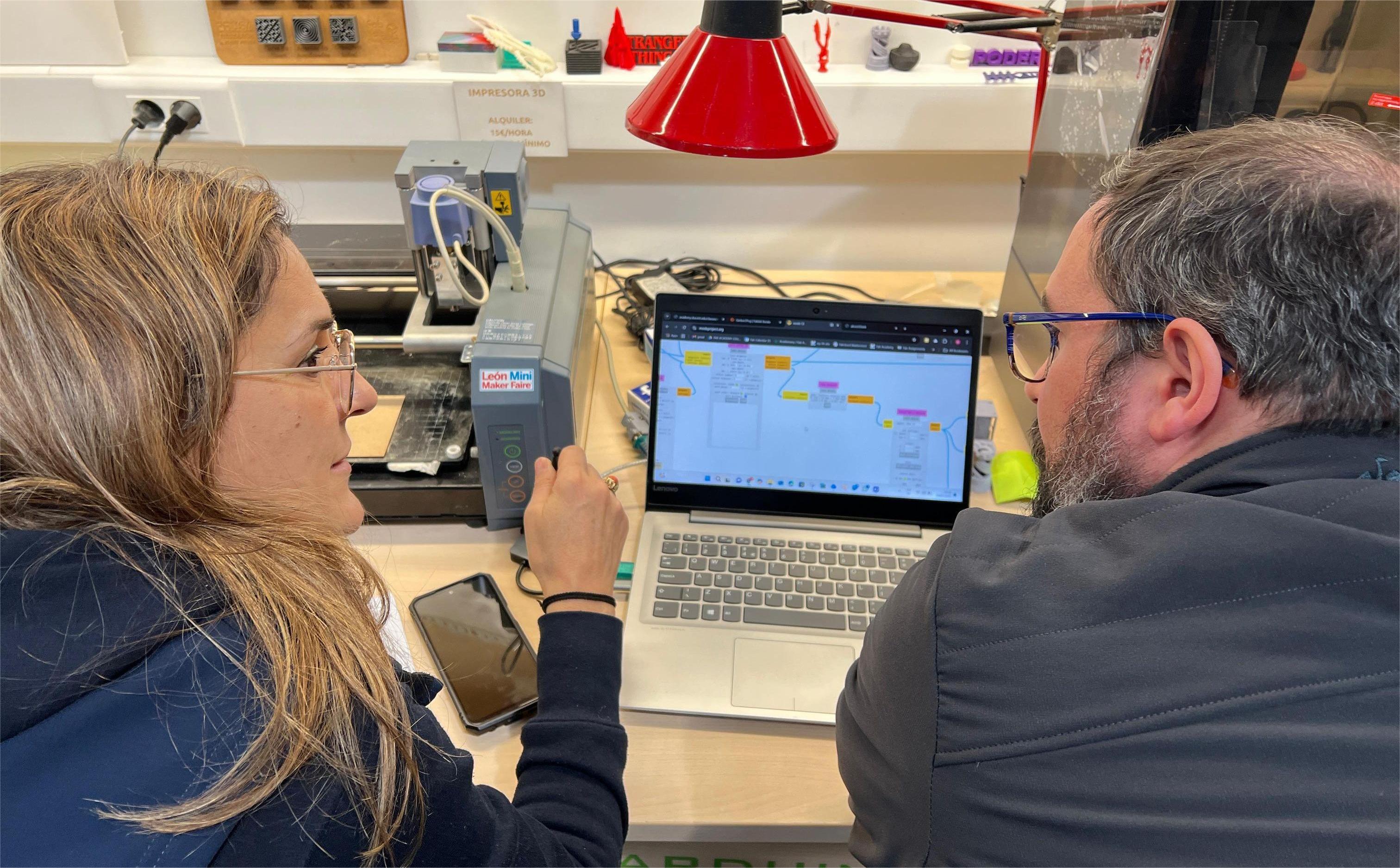
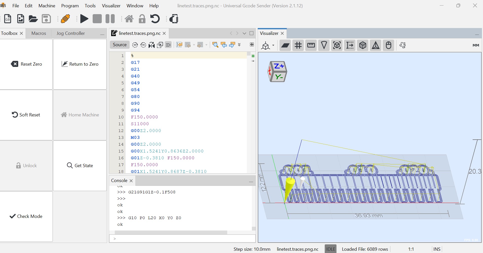
I install Universal Gcode Sender (UGS) and I set up the machine following the steps shown in the Instructor Bootcamp 2024 documentation.
I use the setup wizard to configure the machine. Next, I use Mods to generate the toolpath files and UGS to send the files to the machine.
The bit fitted is a V carve so that is the tool I select in Mods to generate the milling strategy.
In Mods I save the .nc files to machine the line test. I open the traces files in UGS and use the screen controls to move the spindle to the XY origin for the job.
 The Z0 can be set up by lowering the spindle manually and using a piece of paper to ensure the bit is touching the surface of the PCB blank.
Once the xyz origin is set up and the spindle speed controller around 40%, the file can be sent to the machine.
I repeat the process with the outline, this time adding tabs, as the PCB is held by clamps and not stuck with double-sided tape.
Submit a PCB design to a board house
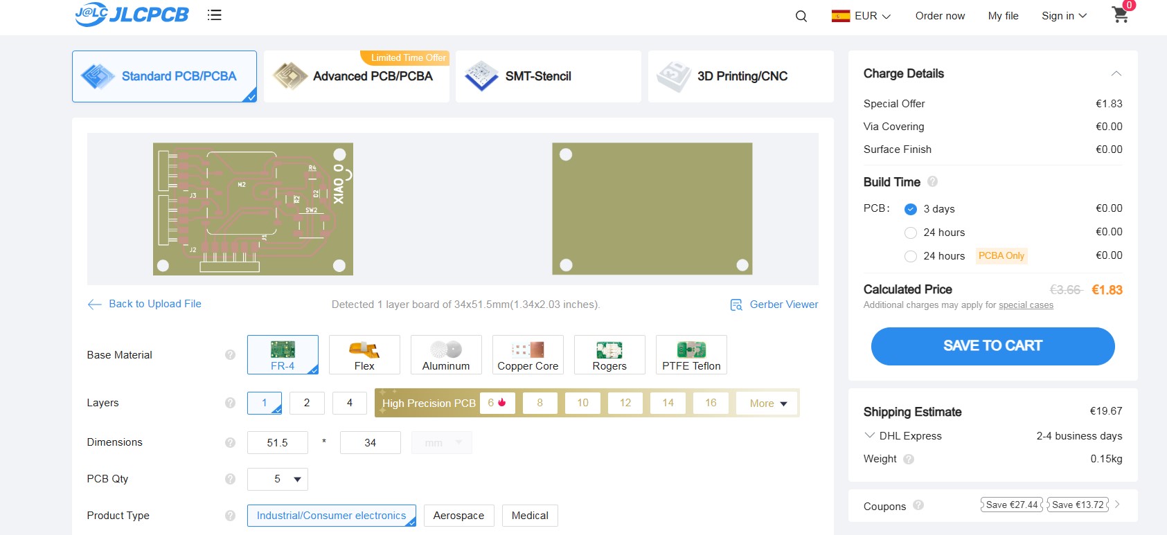
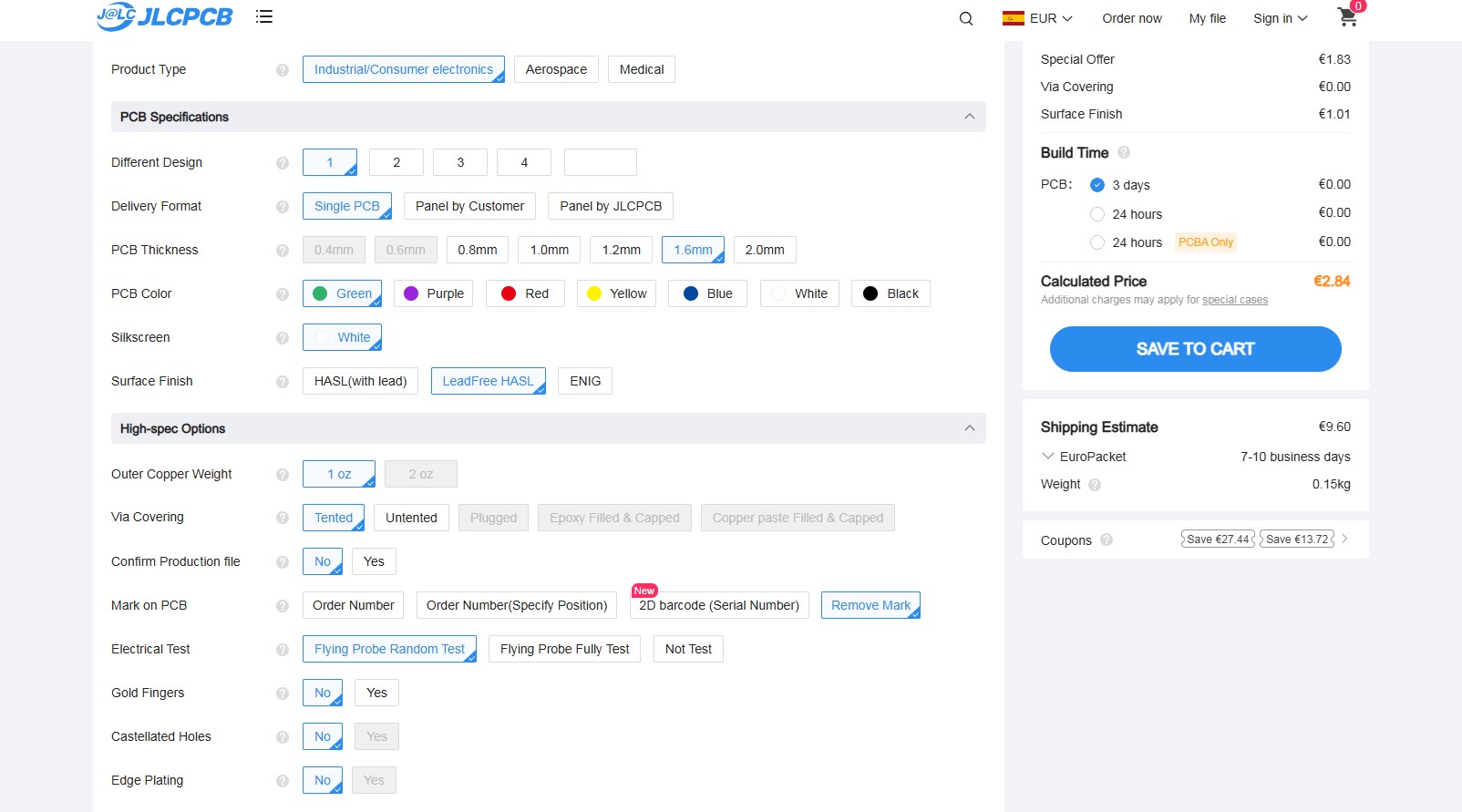
Top
INDIVIDUAL ASSIGNMENT: MAKE AND TEST A MICROCONTROLLER DEVELOPMENT BOARD
FIRST SPIRAL: MANUFACTURING DESIGNED PCB
FILES PREPARATION
After understating the PCB manufacturing process, it is time to manufacture the board I design during Electronics design (Week 06)
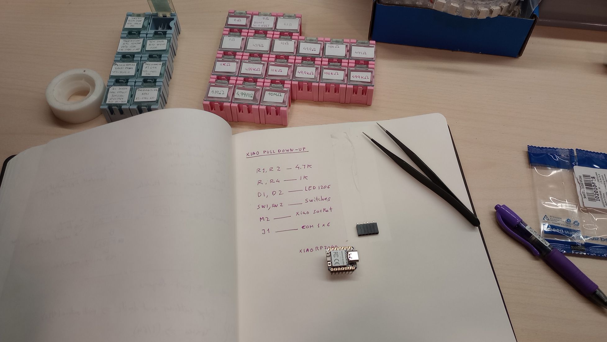
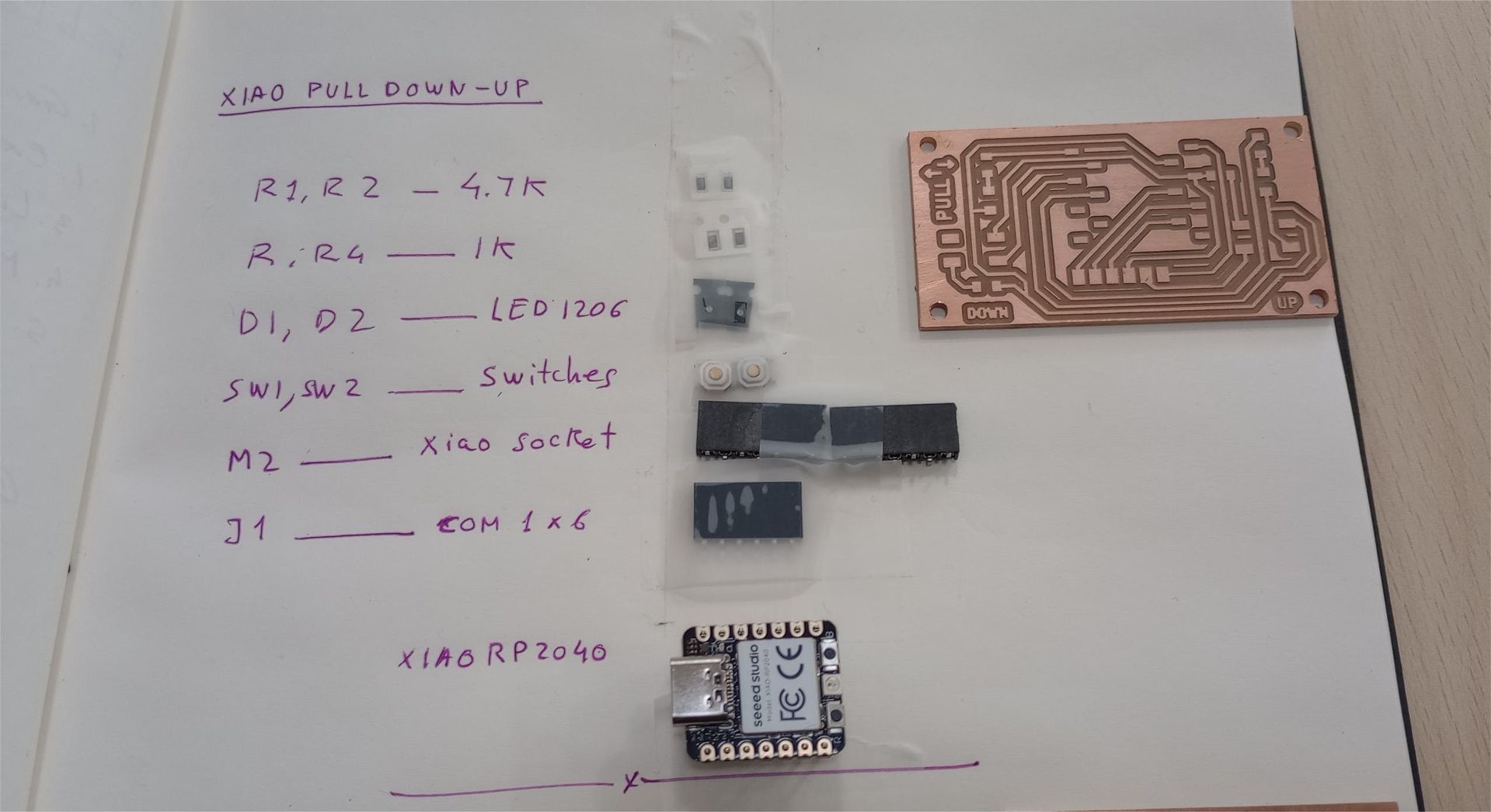
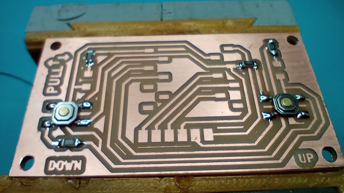
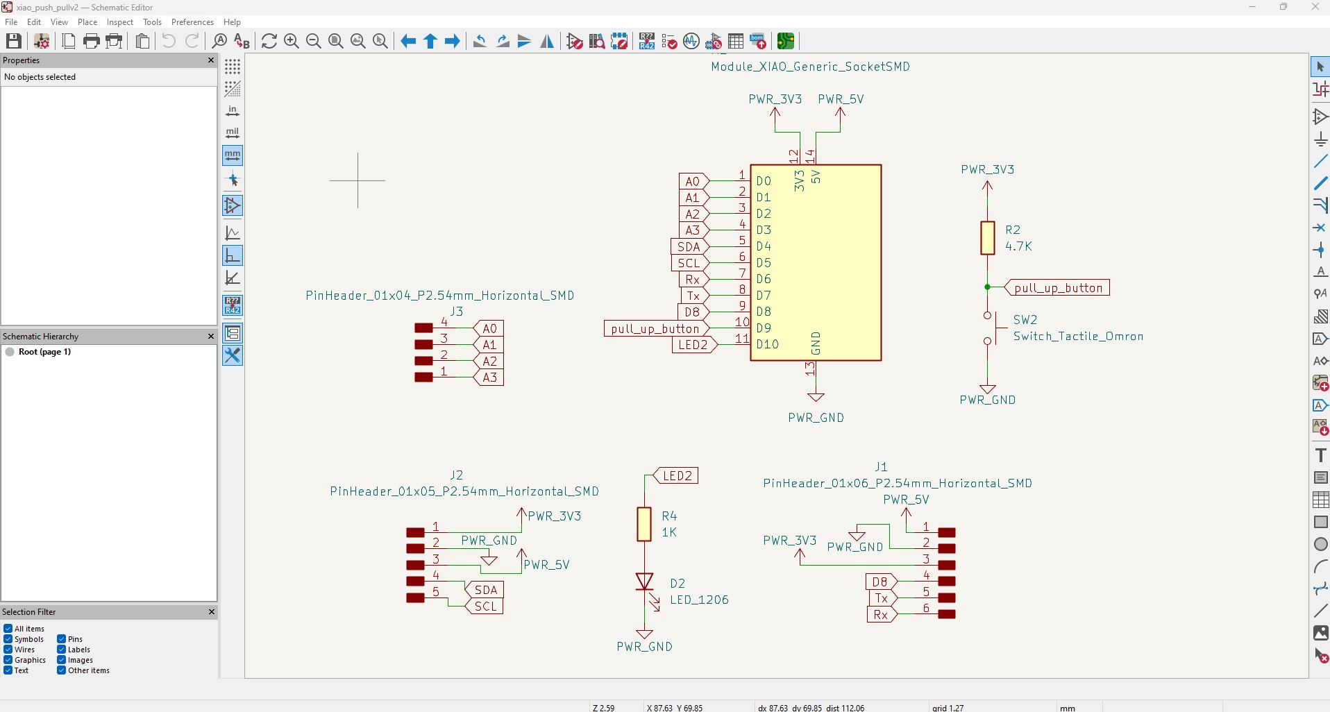
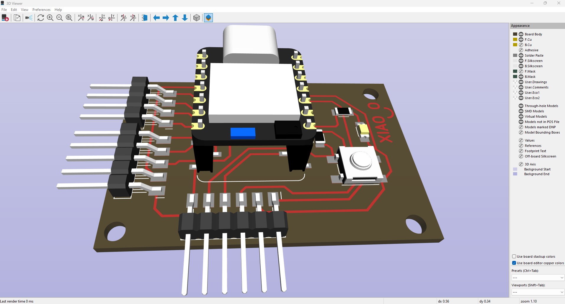
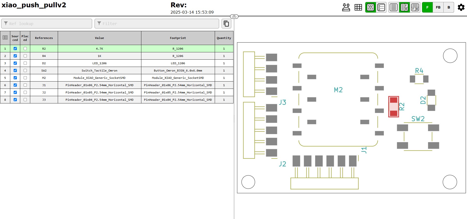
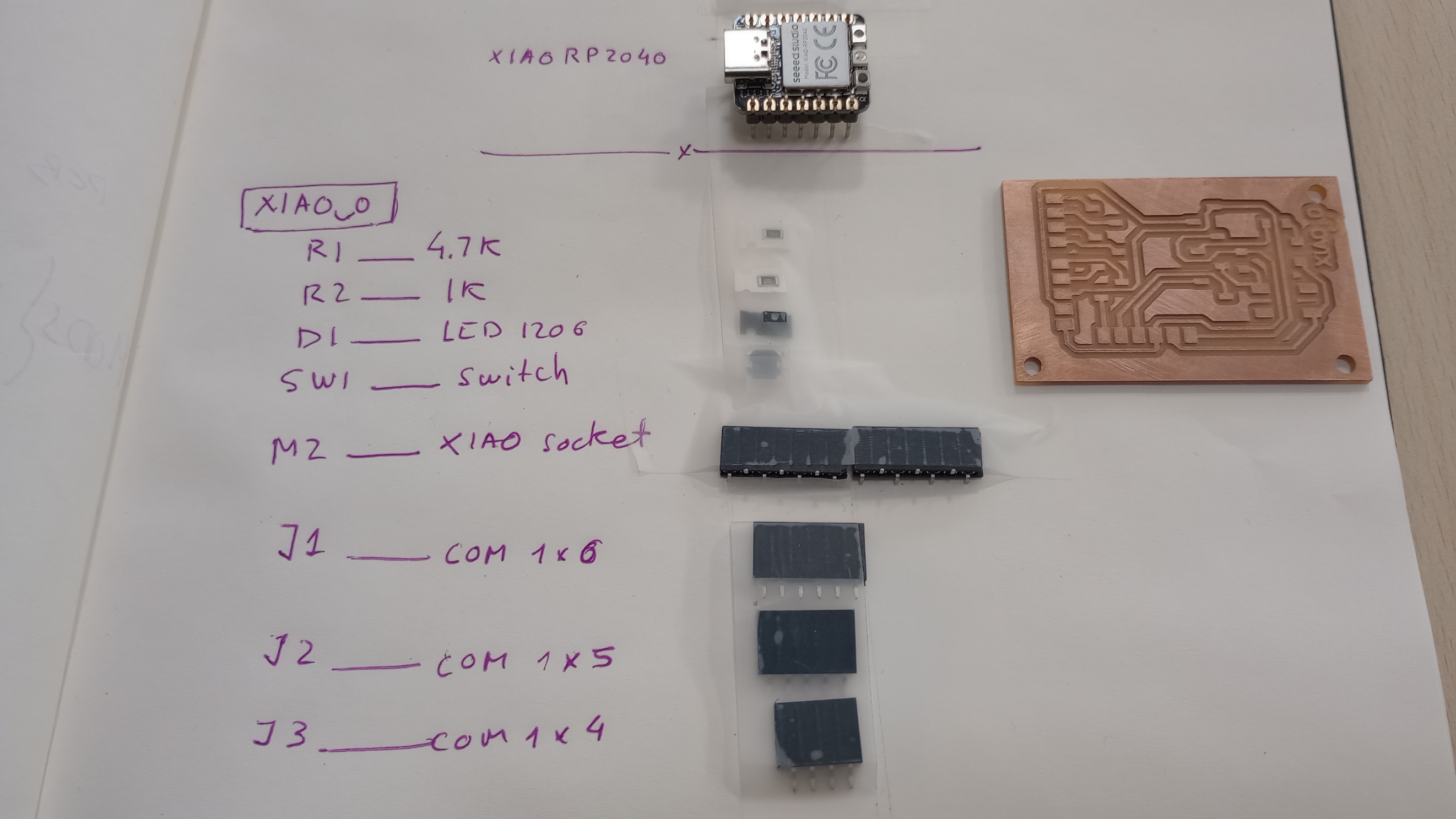
I am milling this board as it is, without any redesigning. If I have time I’ll redesign the board and manufacture the new version too. The board has a pull down and a pull up circuit, a Xiao RP2040, and 6 header pins.
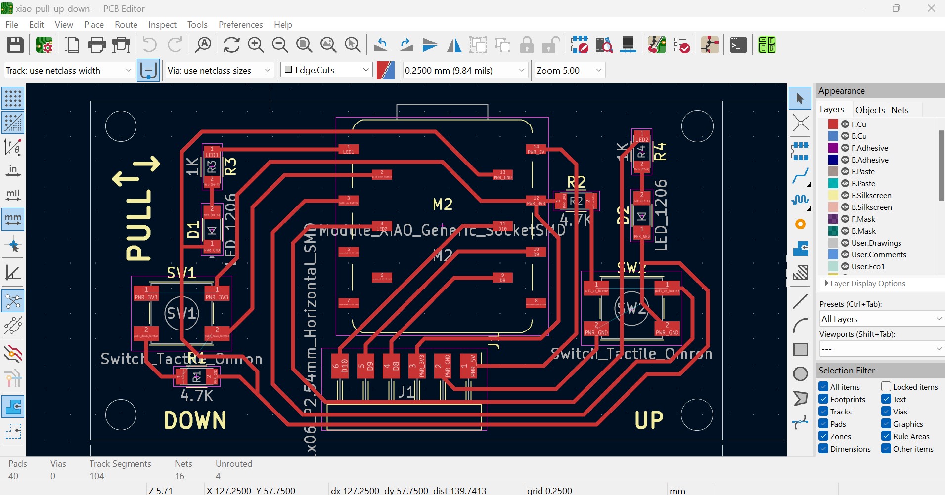
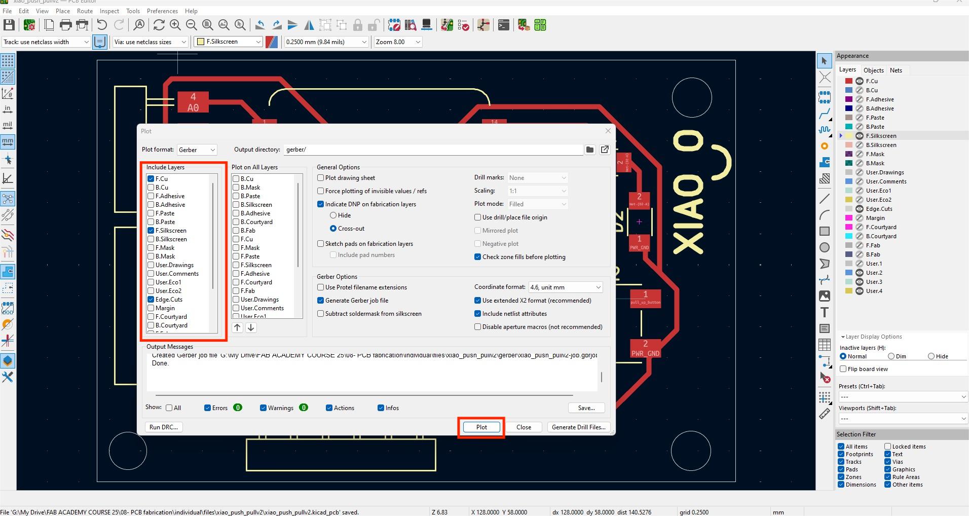
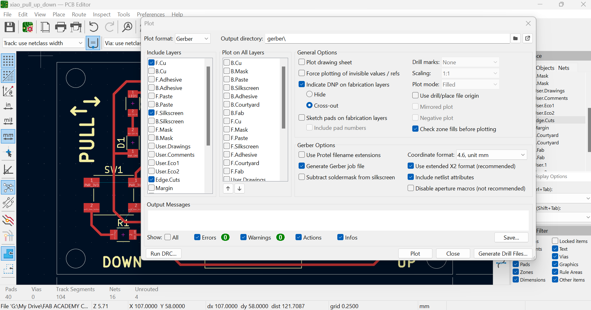
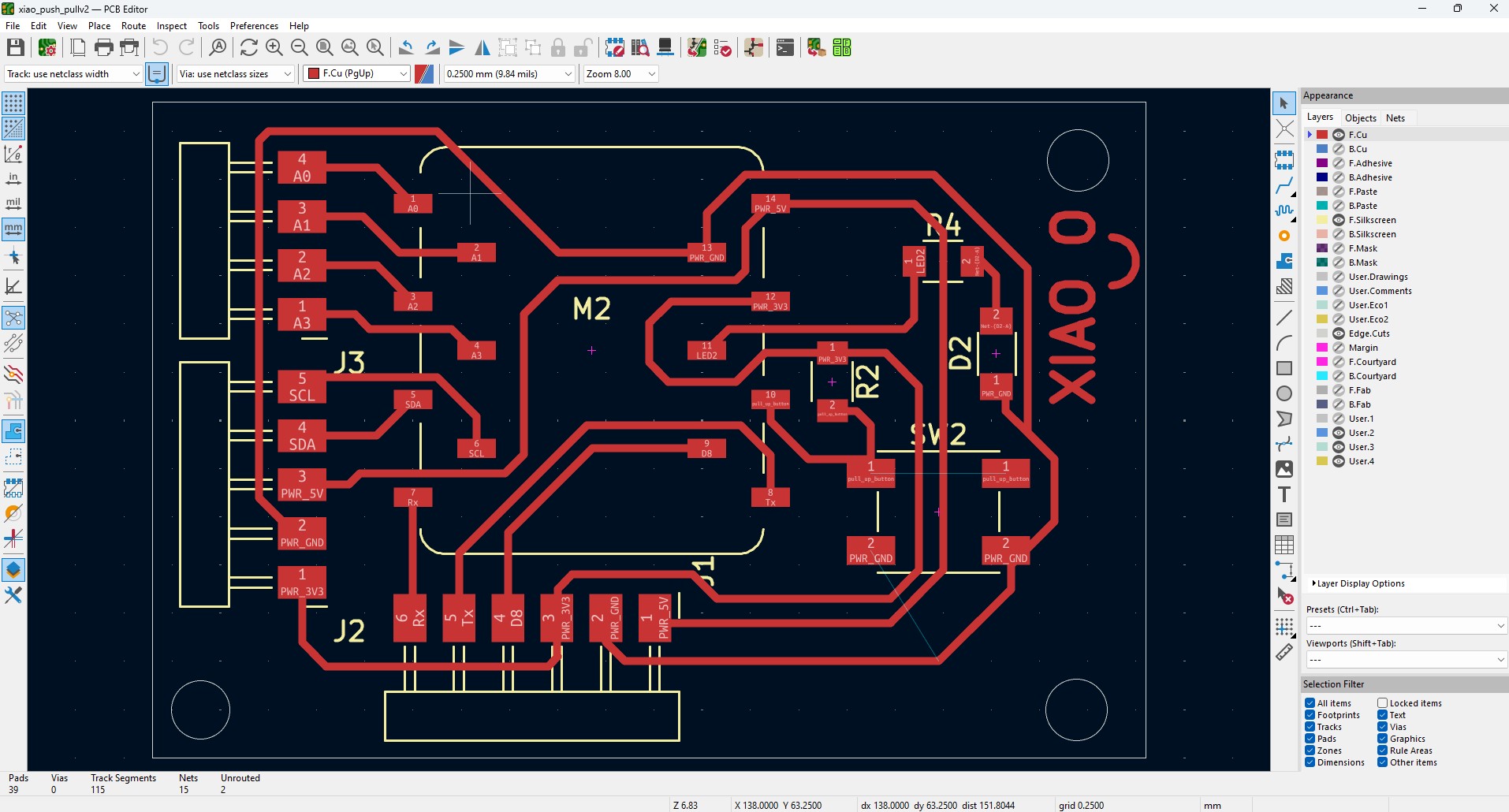
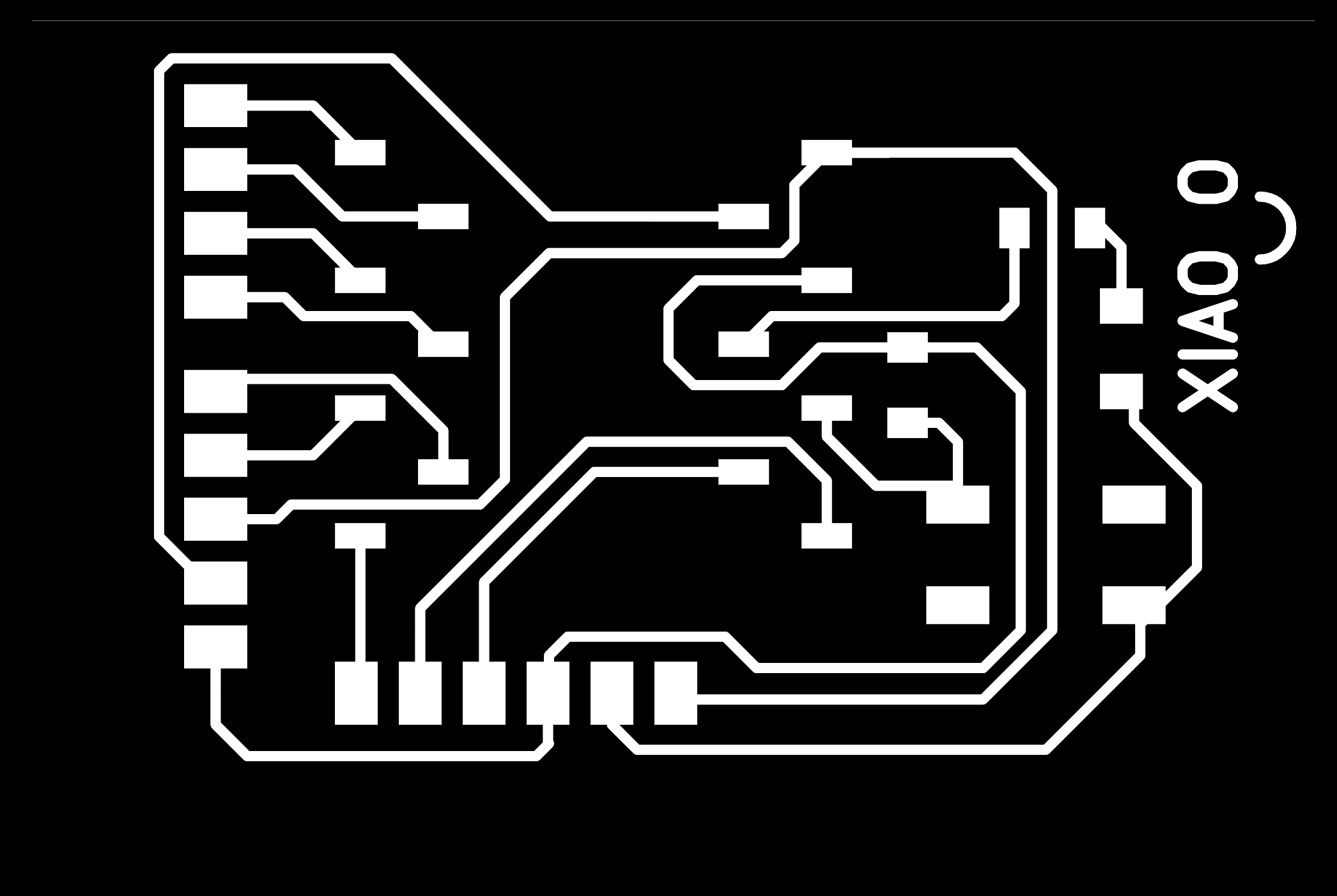
In KiCad9.0 I open the design in PCB Editor. To mill the text I change it to the front copper layer (F.cu) and in File>Fabrication Outputs I export the design using Gerbers (.gbr). If I had through hole components I would have generated the drill files.
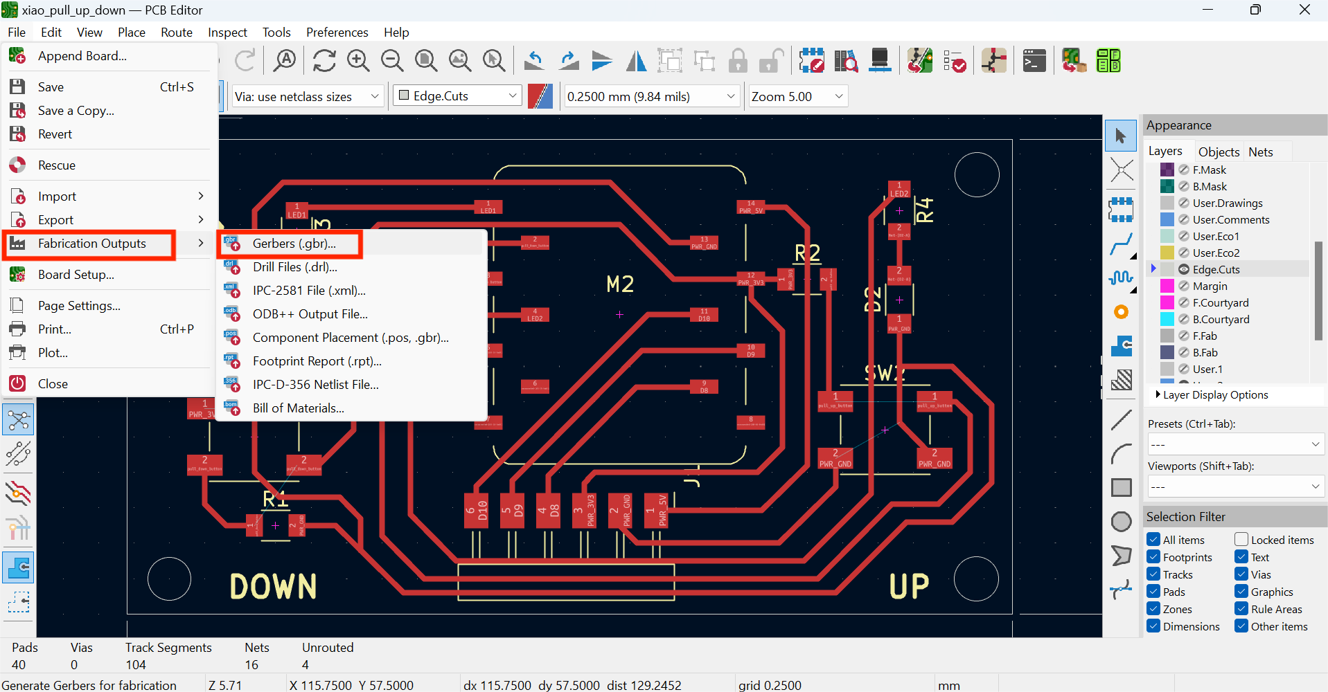
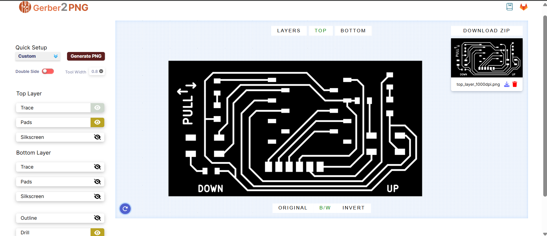
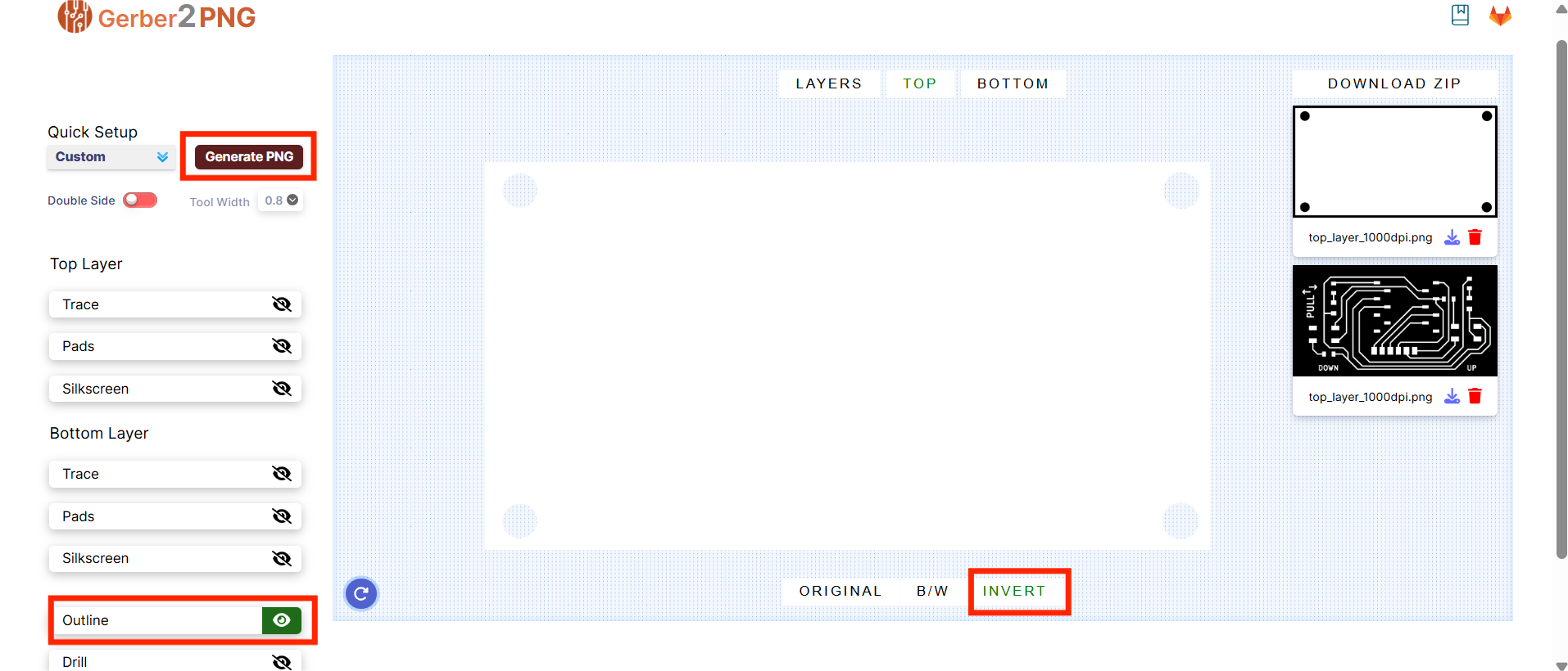
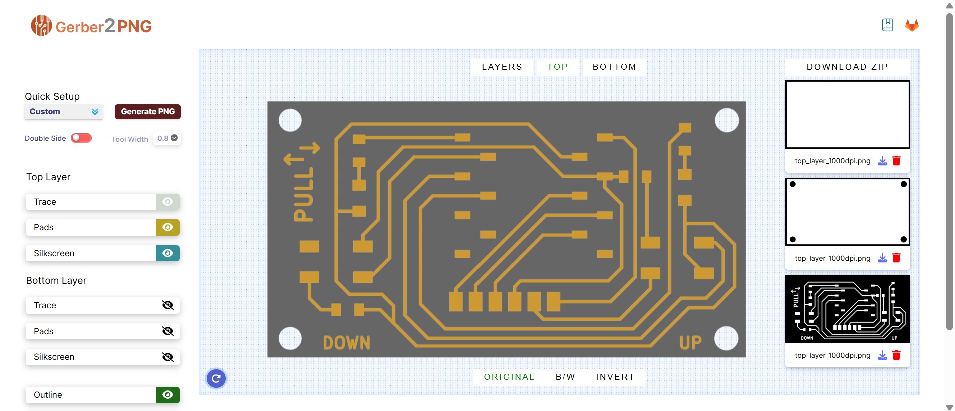
This generates a folder named gerber that contains separate files for each layer. To use this files in Mods I have to convert the .gbr files into png. For this operation I am using the app Gerber2png by Fab Lab Kerala.
In drag the gerber files into the Gerber2png app and the layers and board image is shown.
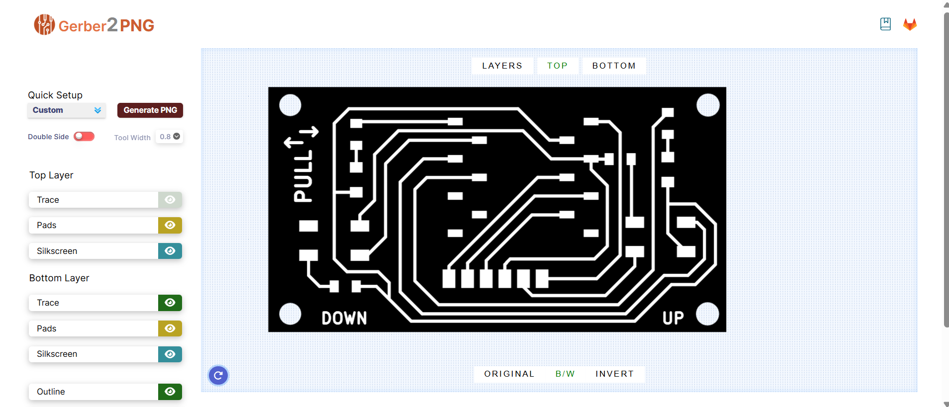
I hide all layers apart from “traces” and I generate the PNG. I repeat the step with the “outline” layer, this time I invert the image before generating the png. To generate the outline border only, I deactivate all layers and invert the image.
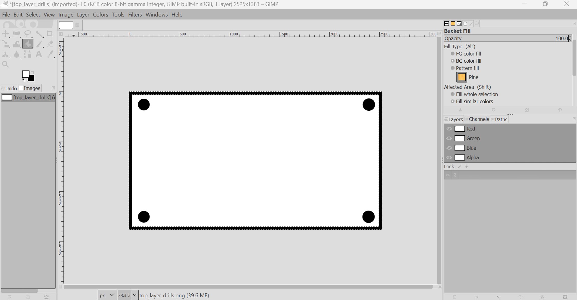
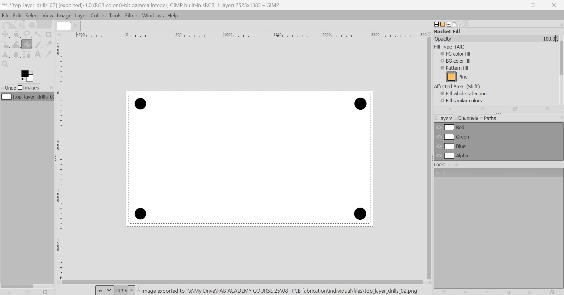
The fabrication process will start with milling the traces, cutting the holes and finally cutting the PCB border. For this reason I removed the border outline from the file with the holes using GIMP.
TOOLPATHS GENERATION WITH MODS AND MACHINE SETUP
From here, I follow the workflow explained in the group assignment to mill the board with the Roland Modela MDX-20A. In MODS I load the traces png, select the Mill traces strategy, select the work origin and Calculate the mill raster.
The process will be repeated for each file and sent to the milling machine after the previous one has been machined.
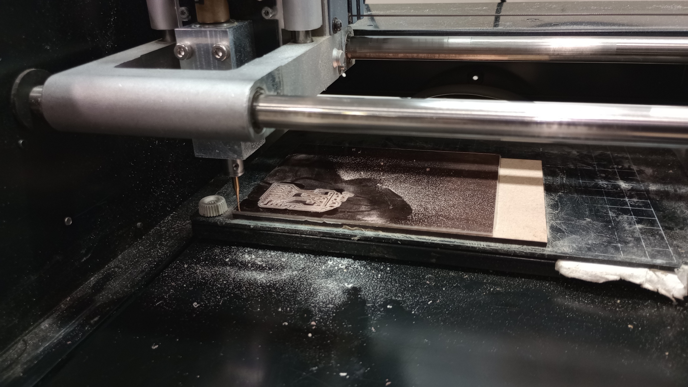
I use double-sided tape to stick the PCB blank on top of the sacrificial piece
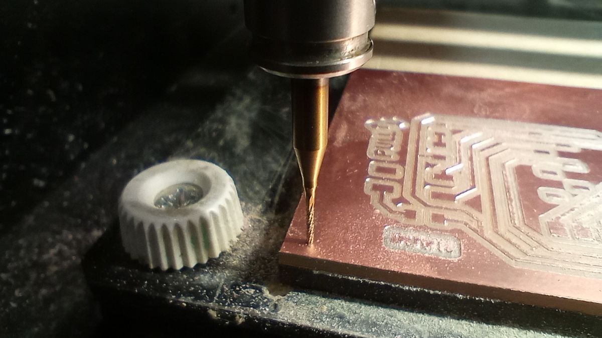
I fit the conical ball nose end mill with 0.25 radius and I set up Z0 as explained the group assignment. The traces file is ready to be sent.
PCB MILLING
The traces are machined first. Some copper burr is shown on the traces; this will be removed later.
Next, I remove the milling bit and load the cutting end mill. I set up Z0 again for this bit, which will cut the holes and the PCB outline.
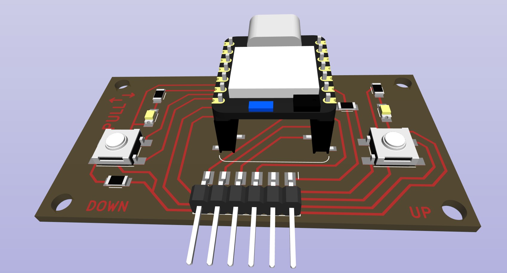
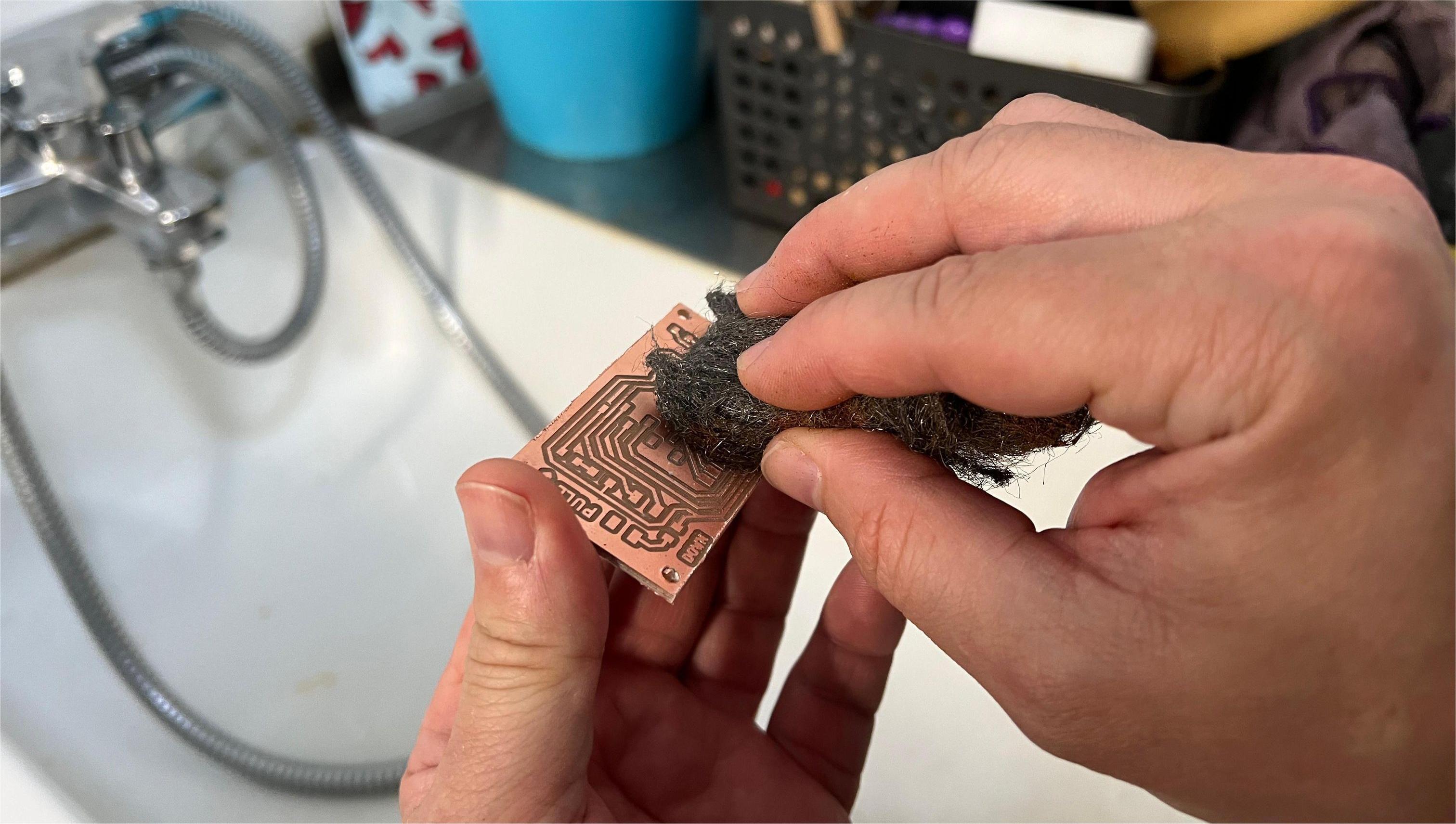
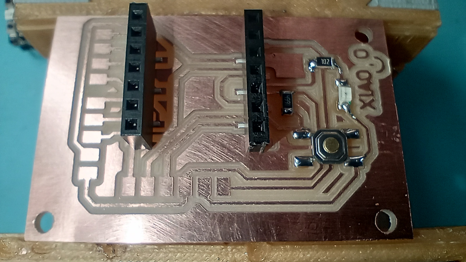
Once the the milling operations are completed I remove the board and I polished it using steel wool
SOLDERING COMPONENTS
On my notebook I make a list of components required for the PCB. With Adrián's help I select the components and use tape to stick them next to their name.
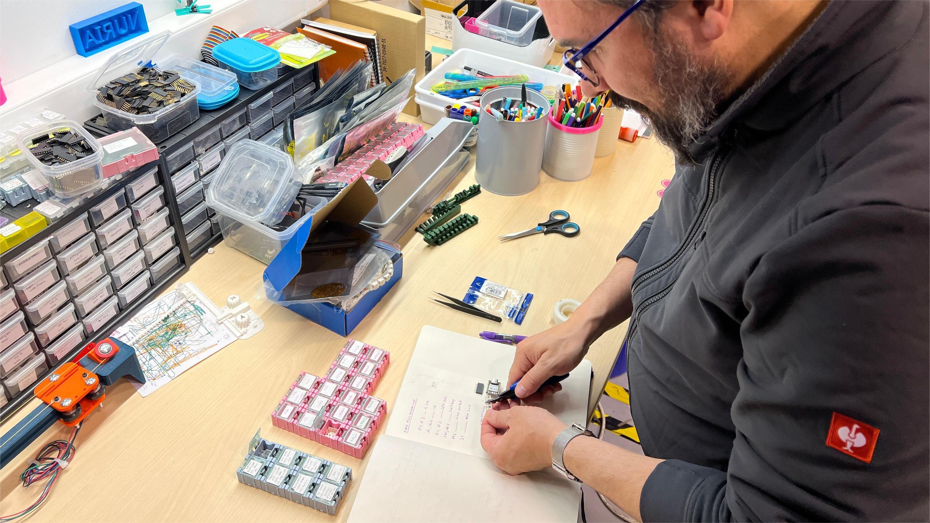
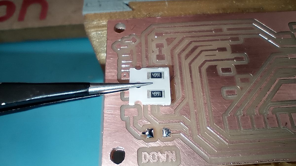
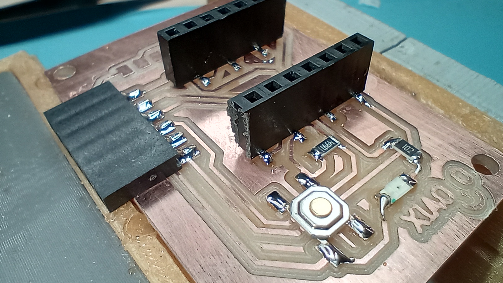
I use a vice to hold the PCB, tweezers to pick the components, a soldering magnifying glass and the soldering station with a clean tip. I start by tinning the component pads, then placing the component, melting the solder to secure the component and adding more solder. This takes a bit of practice and I made a few mistakes, such adding too much solder, pre-tinning both pads of a component, or loosing one of the tiny LEDs.
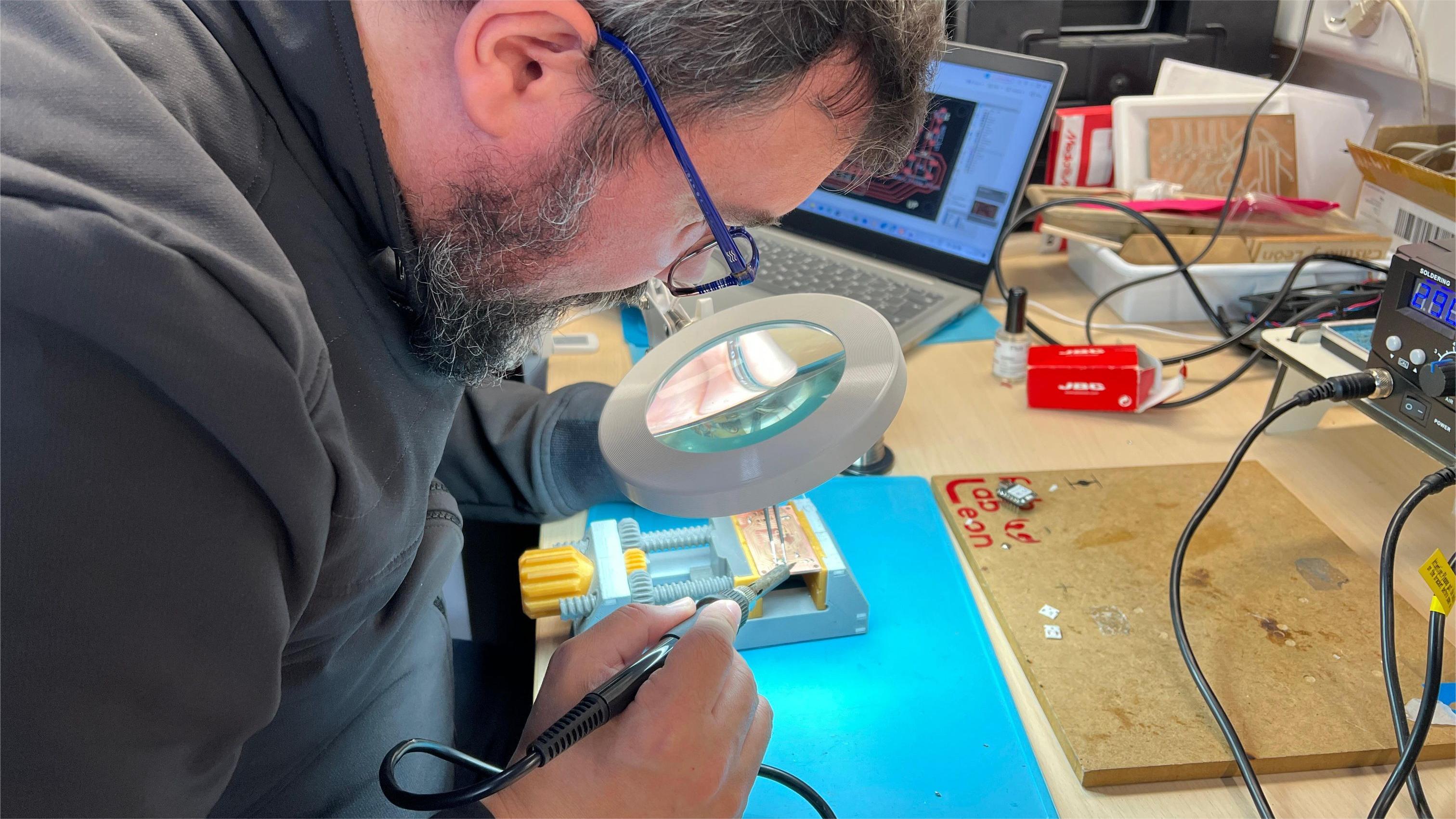
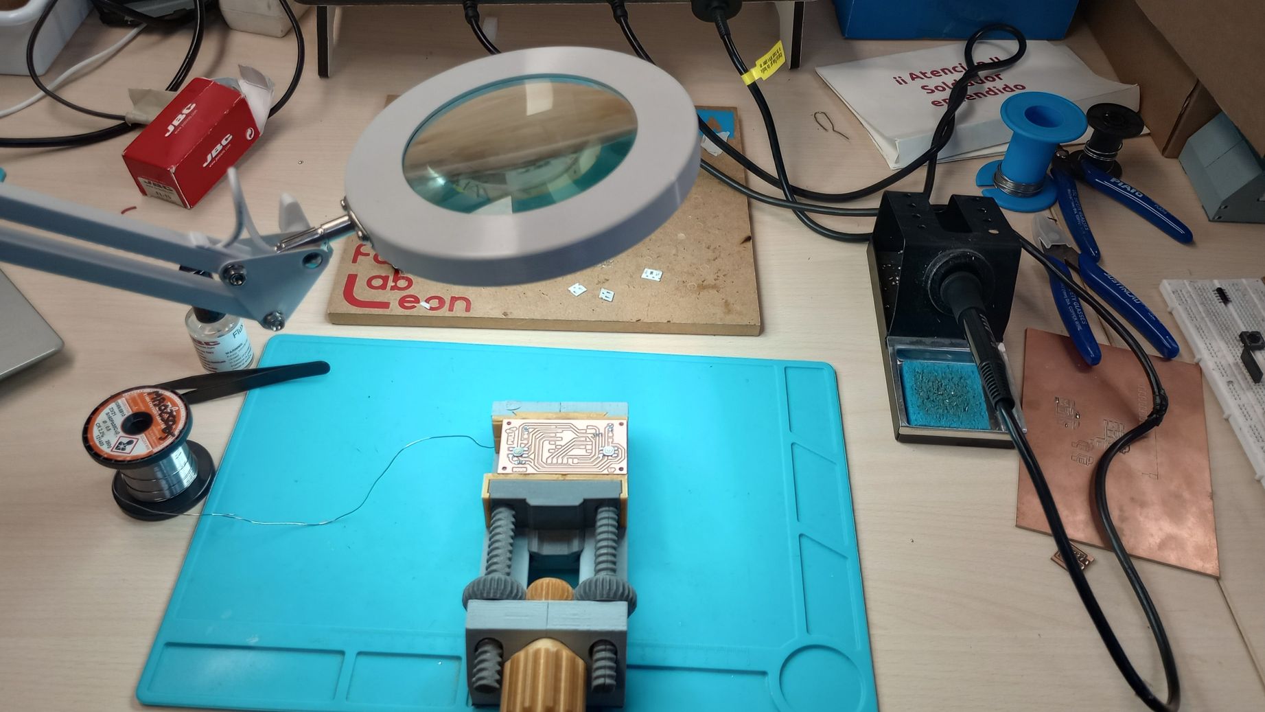
I start by populating the smaller components, leaving the sockets and header pins for last. I also ensure that the LEDs are placed with the correct polarity according to the circuit design.
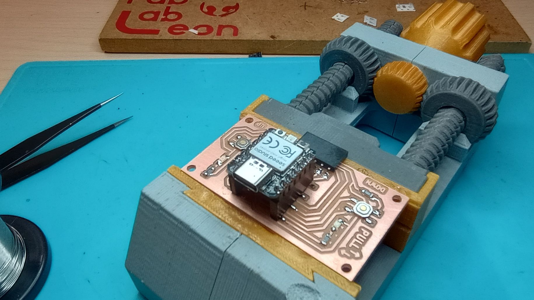
TESTING THE DEVELOPING BOARD
Everything looks good, but it's time to use the multimeter to test some components. I check the continuity of tracks, and with the multimeter in diode mode, I verify that the LEDs light up.
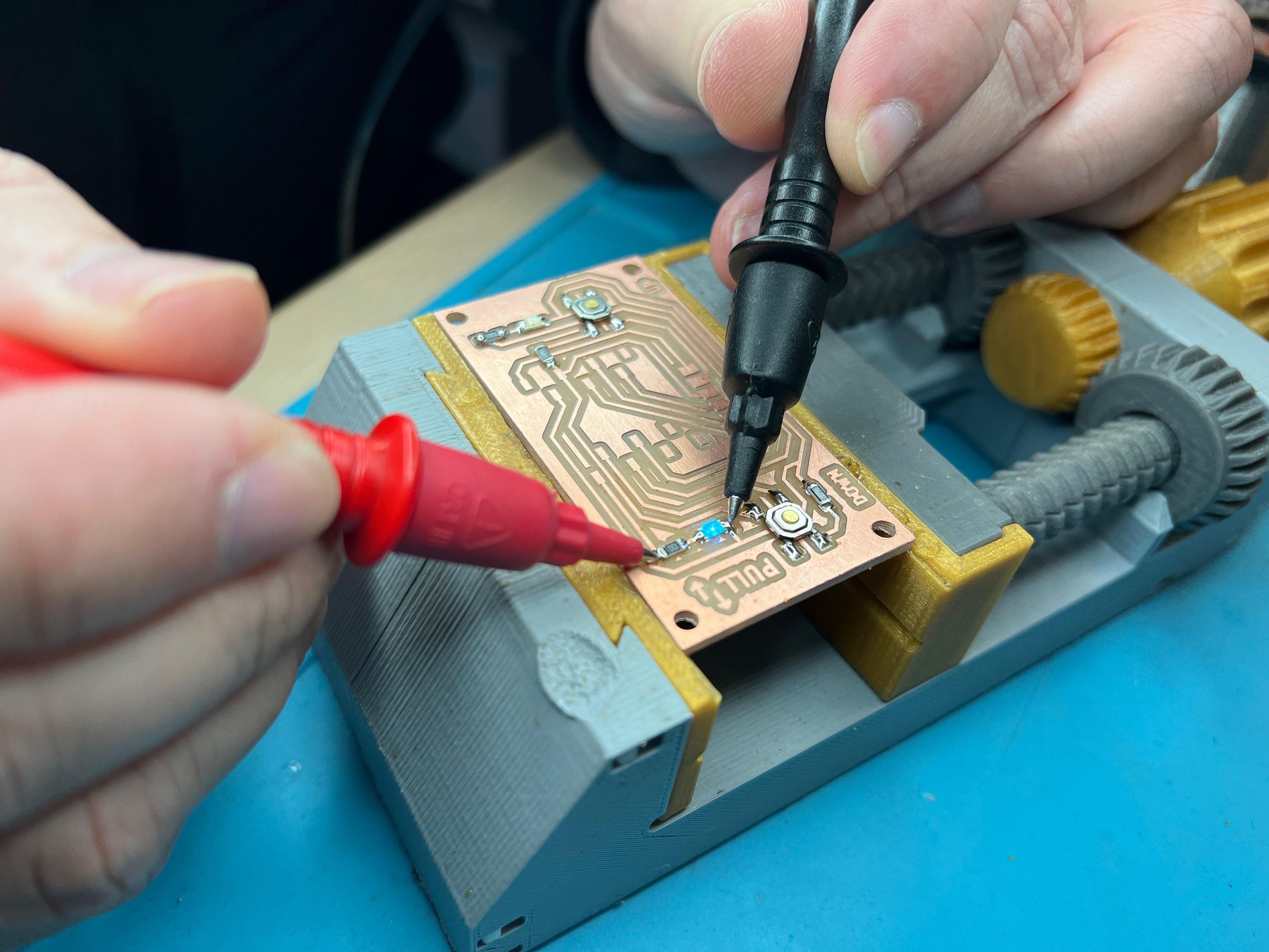
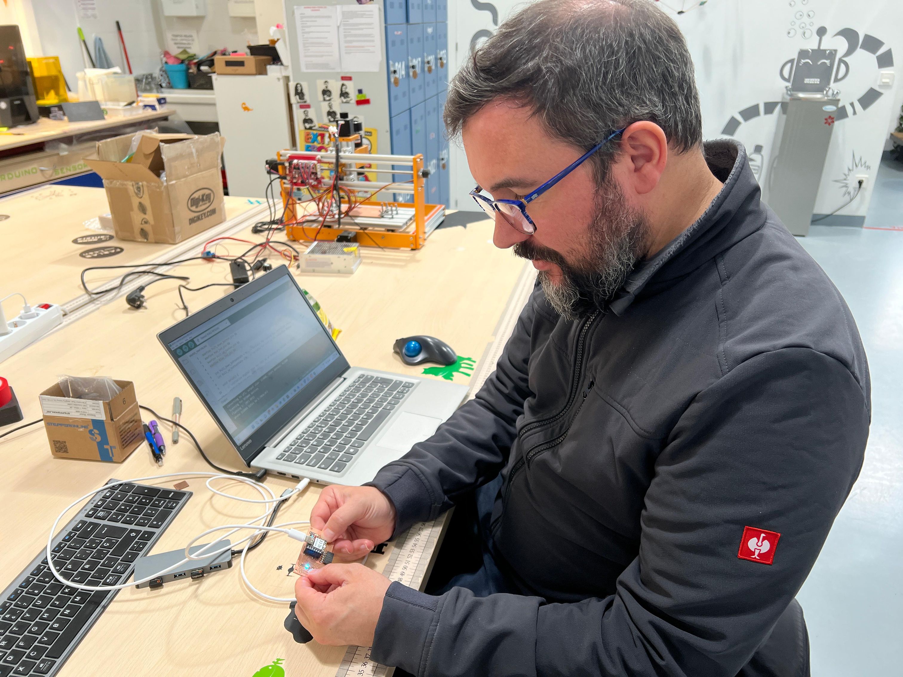
With the XIAO connected to a laptop I check the voltage reading in the 3 and 5V outputs.
Finally, I loaded the program I used to simulate the circuit during week 06 to test that the development board works correctly.
Top
SECOND SPIRAL: REDESIGNING AND MANUFACTURING PCB
PCB REDESIGN
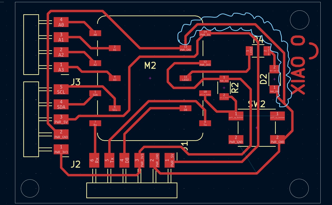
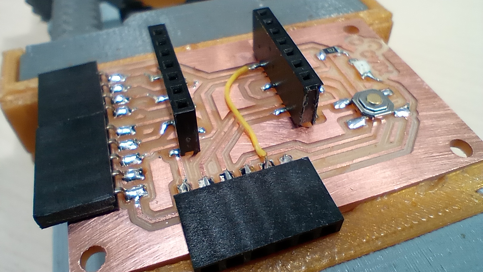
Starting with the design of the development board fabricated before, I designed and produced a new development board. The aim with this board was to have access to the 4 analogue pins of the XIAO RP2040, provide connection to Rx a Tx pins to transmit data, and any other available pins. To have more pins available I decided to remove the pull down circuit from the previous board.
PCB MILLING
I follow the workflow outlined for the Roland Modela when preparing and fabricating the file. Additionally, I select and solder the components using the same approach as before.
SOLDERING
During testing of the board with a multimeter, I noticed that there was no voltage reading on one of the pin header connectors. Upon checking the design, I realized that I had forgotten to connect a ground (GND) track to one of the header connectors. The solution was to use a wire to connect the pins.
TESTING
USEFUL LINKS AND RESOURCES
FILES
KiCad 9.0 Model of PCB XIAO_O: xiao_board_v2_kicad9.zip
Arduino test program for XIAO_O: XIAO_O_test.ino
PNG files of traces edge and drills: png_traces_edge_xiao_o.zip
Top