Week 06. Electronics Design
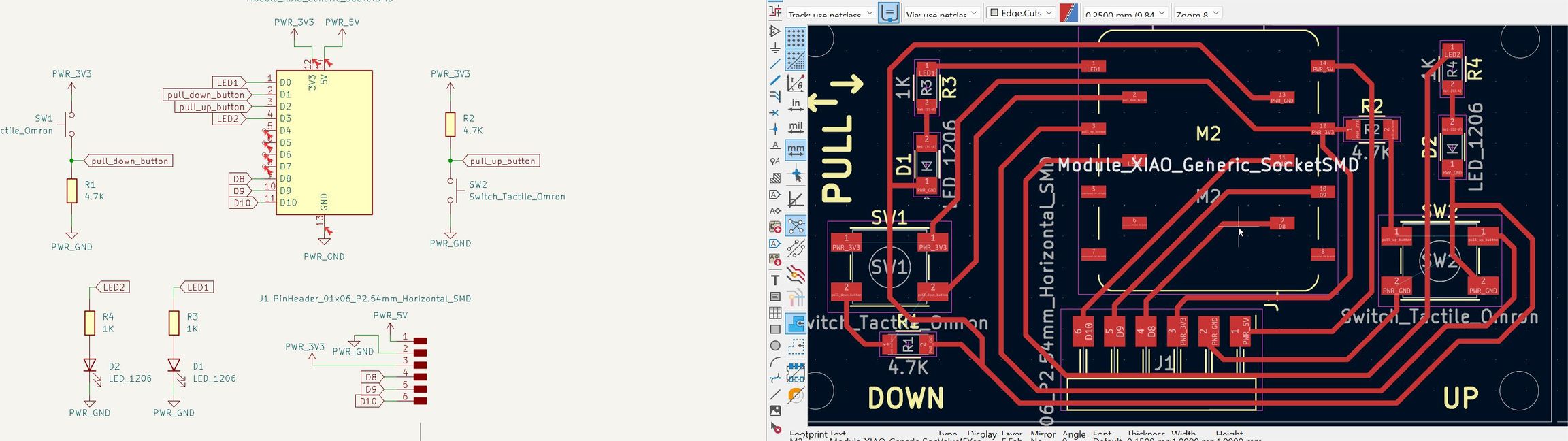
Table of Contents
- WEEKLY PLAN
- GROUP ASSIGNMENT: ELECTRONICS TEST EQUIPMENT
- INDIVIDUAL ASSIGNMENT: ELECTRONICS DESIGN
- USEFUL LINKS AND RESOURCES
- FILES
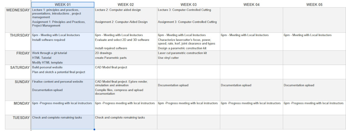
WEEKLY PLAN
Group assignment:
- use the test equipment in your lab to observe the operation of a microcontroller circuit board
Individual assignment:
- use an EDA tool to design a development board that uses parts from the inventory to interact and communicate with an embedded microcontroller
- extra credit: try another design workflow
- extra credit: simulate your design
- extra credit: design a case around your design
GROUP ASSIGNMENT:ELECTRONICS TEST EQUIPMENT
This is the link to the Fab Lab León Group Assignments page. Since I am completing the group assignment on my own I left the documentation on this page.
This week’s assignment consists of using electronics testing equipment. In Fab Lab León I have access to a multimeter, an oscilloscope and a logic analyzer. Each of these tools plays an important role in testing and diagnosing electrical circuits.
MULTIMETER
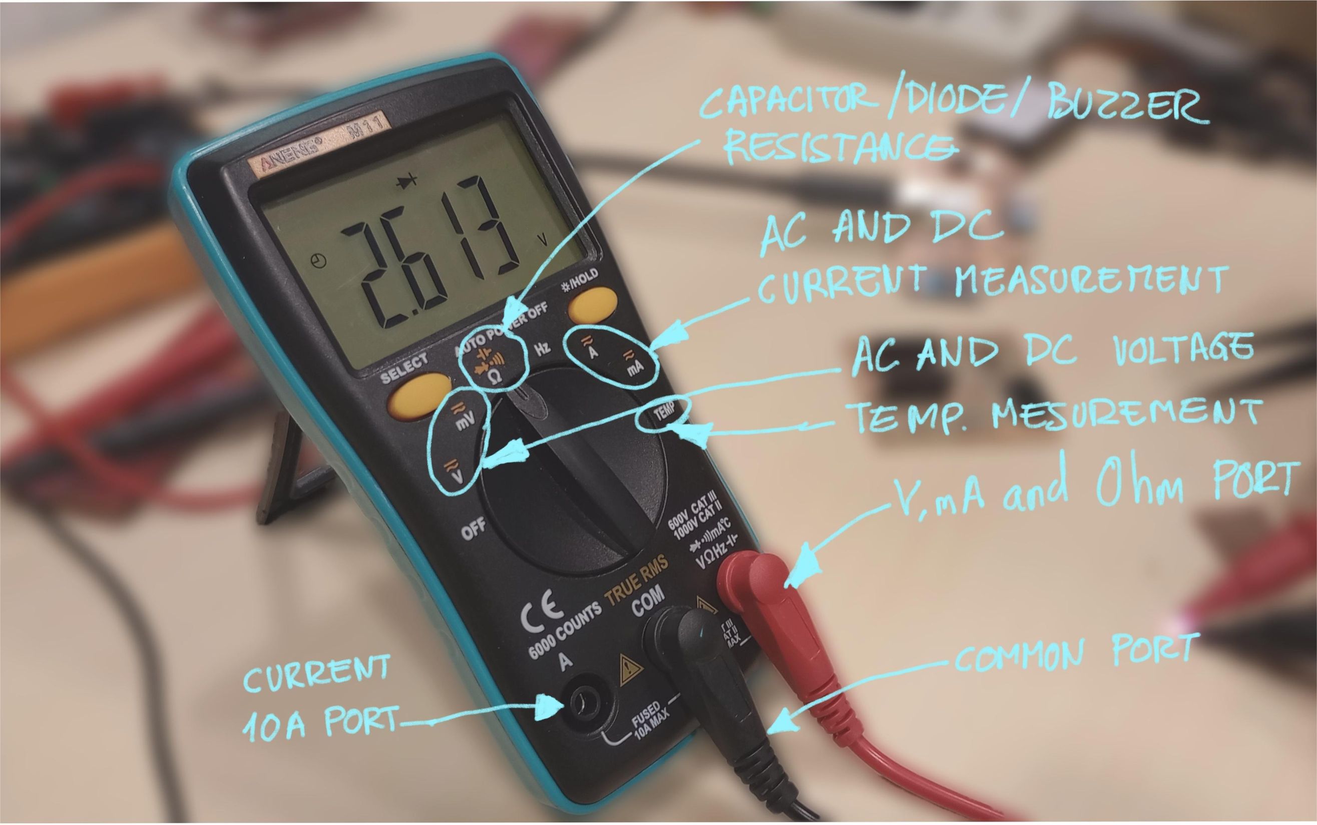
A multimeter is an electrical instrument to measure different electrical magnitudes, such as voltage, current and resistance. It is like the Swiss Army knife electronics as it is useful for testing components, troubleshooting circuits and testing for continuity.
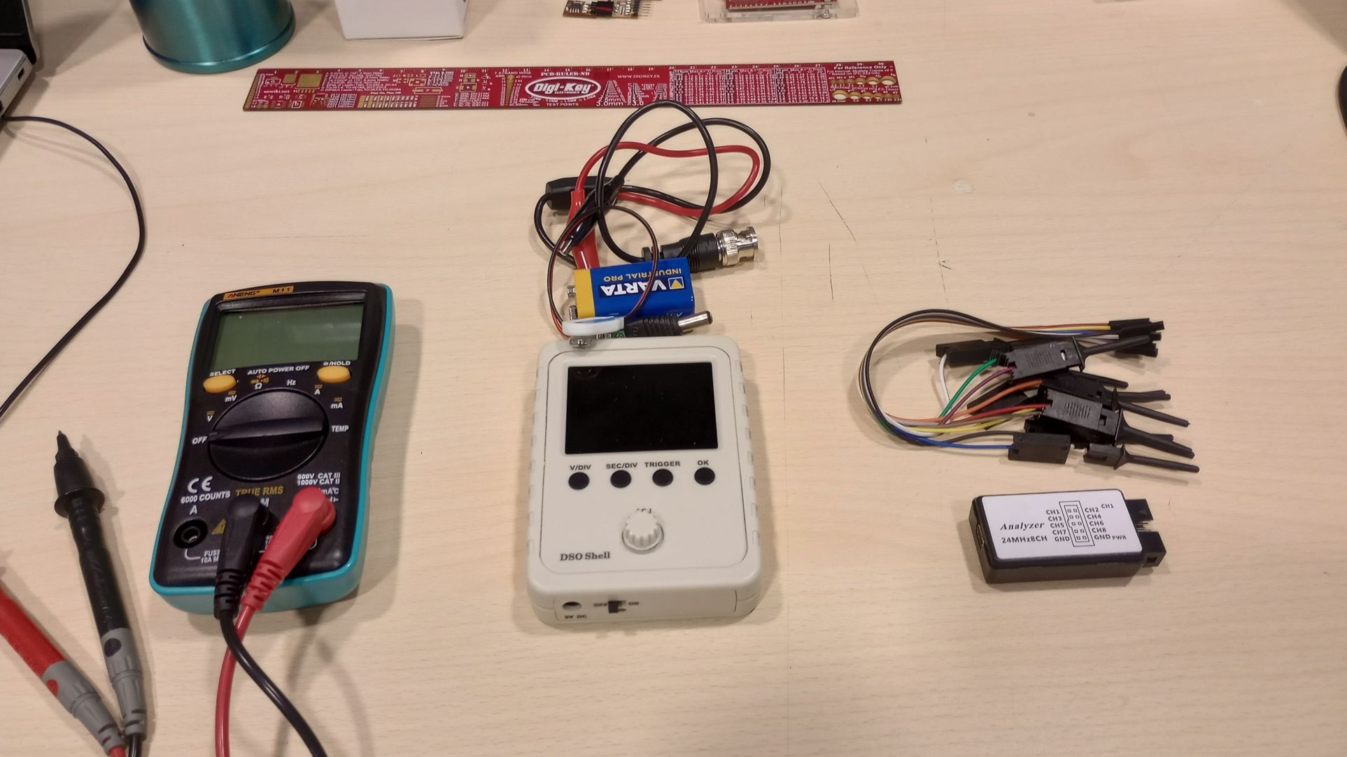
For the following tests I am using the digital multimeter ANENG M11
Component Testing: The multimeter can be used to check individual components like resistors, capacitors, and diodes to confirm whether they are functioning properly.
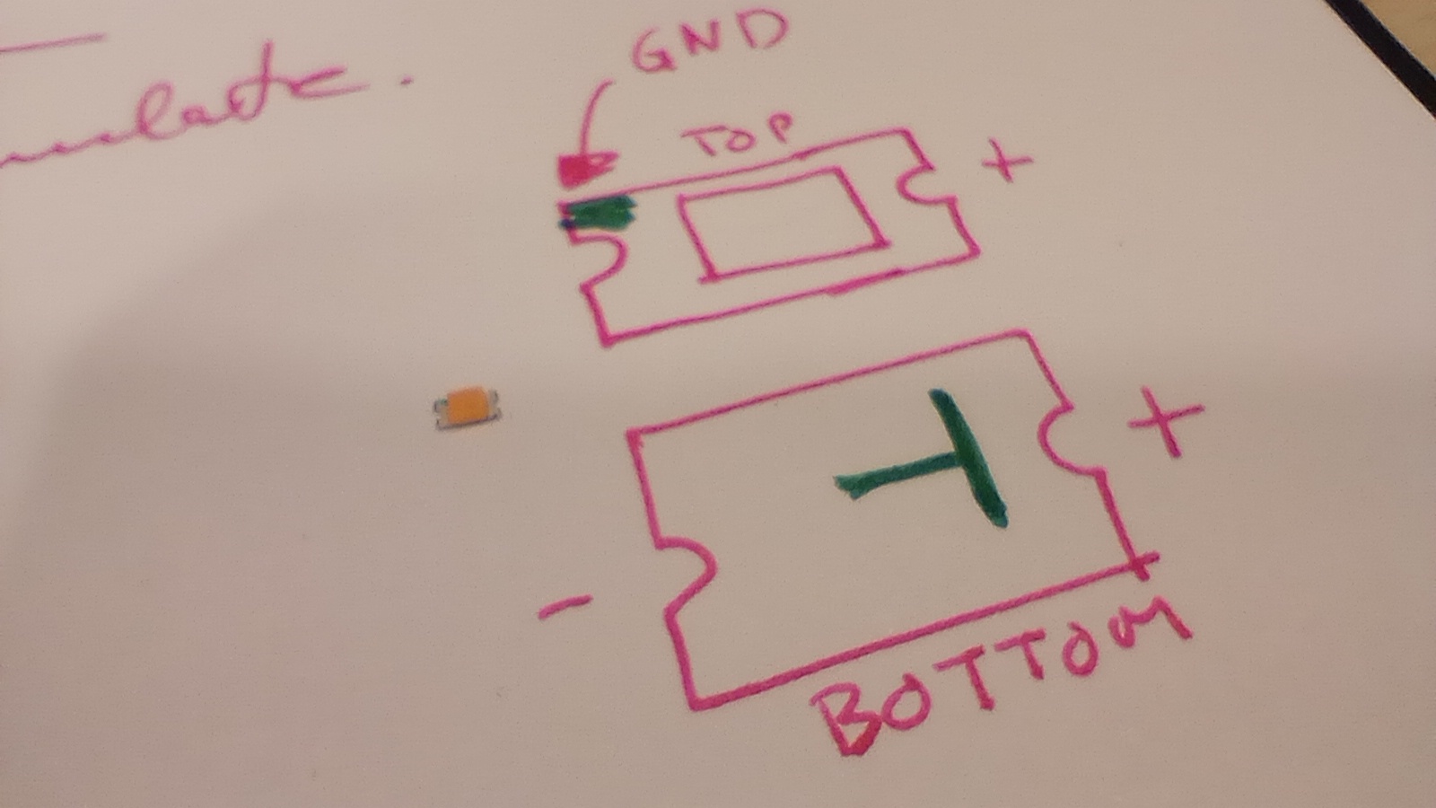
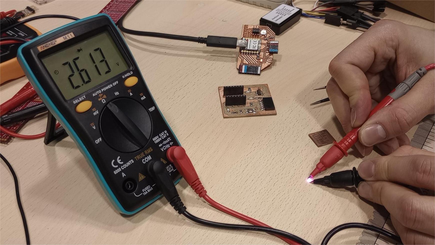
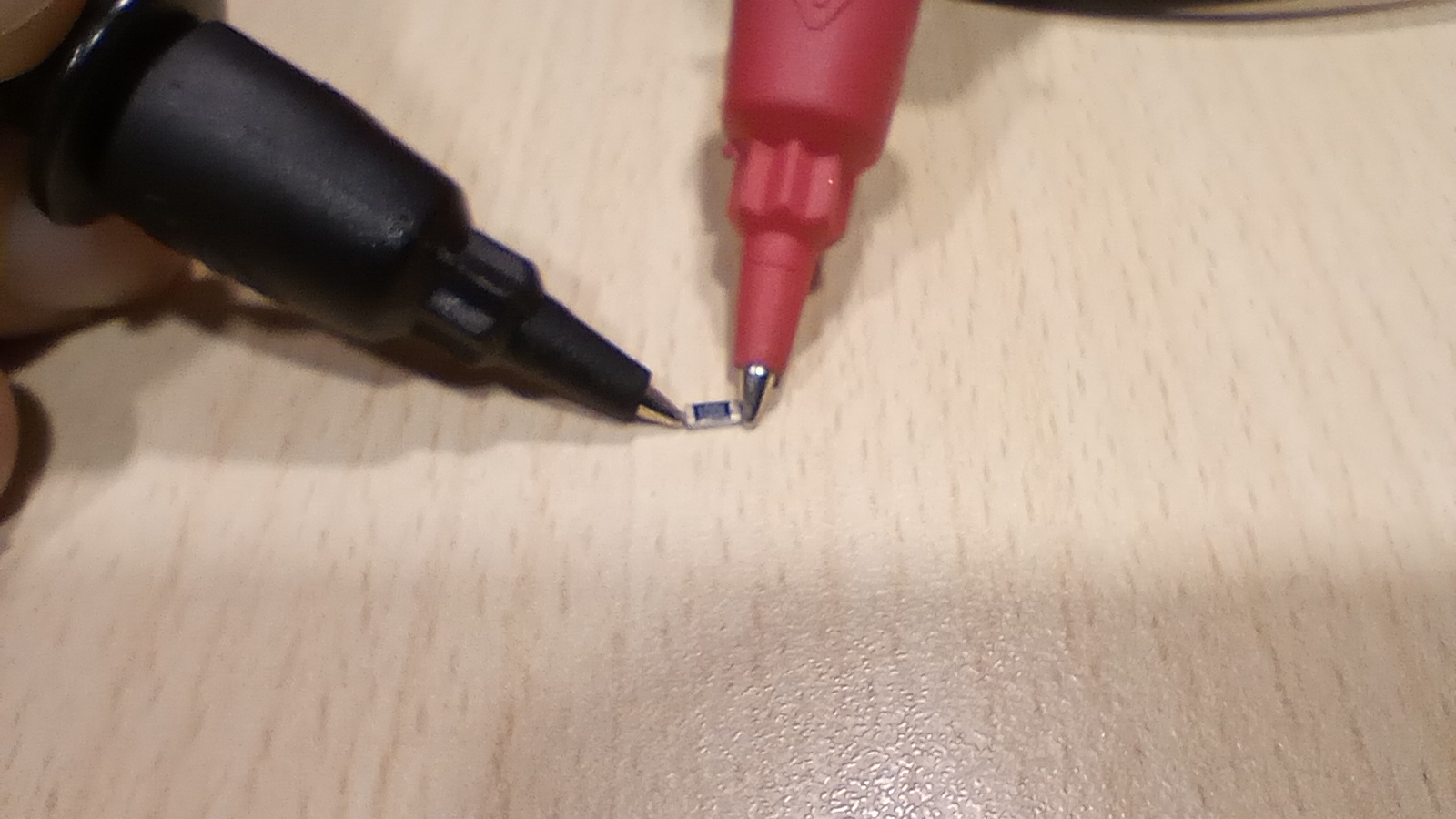
Here I am testing the correct functioning of a SMD 1206 LED. It is important I probe the LED correctly, identifying first the cathode and anode. In the diode mode of the multimeter, I connect the red probe to the anode and the black one to the cathode. The multimeter displays a voltage drop of 2.613v and the LED lights up.
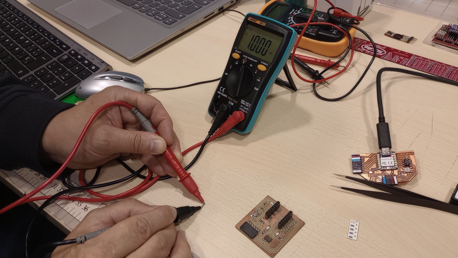
Next, I use the multimeter to read the value of a SMD 1206 resistor. I have the multimeter in Auto mode and it displays a value of 1.0 KΩ.
Continuity Testing: The multimeter can also be used to check if there is a continuous path for current in the circuit, which helps in detecting broken connections or wires.
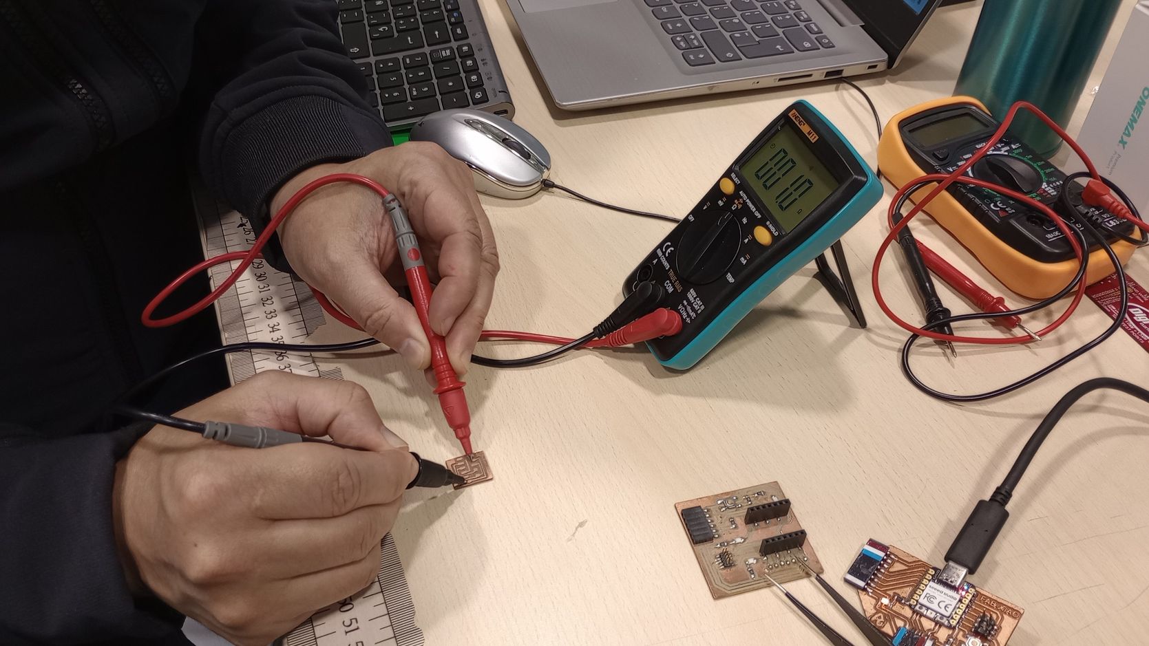
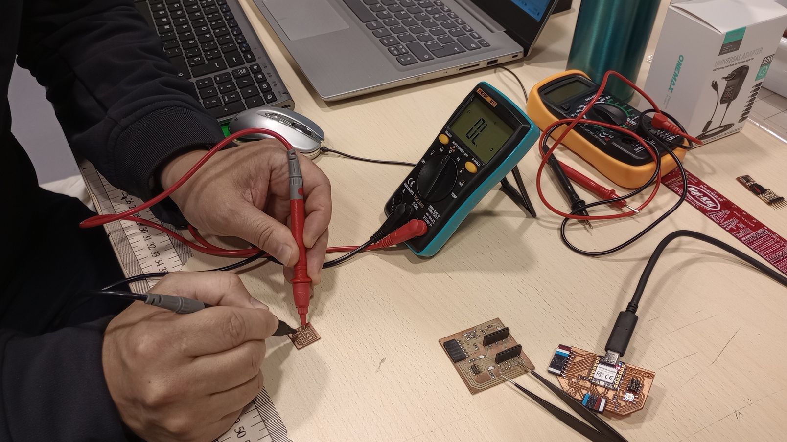
Here I show how I am testing the continuity of the tracks on a PCB. The display shows 1 when there is continuity and 0L when there is no continuity, in this case because I am probing on different tracks.
Troubleshooting Circuits: The multimeter helps diagnose issues in a circuit by measuring voltage and current levels, ensuring they are within expected ranges.
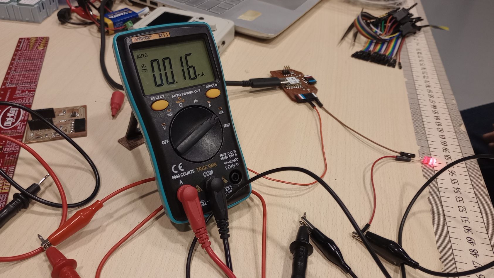
I am testing the current on a fading LED connected to a Xiao development board. First, I move the red proving lead into the 10A current port, and the dial to the mA setting.
Next, I use jumper wires to “break” the circuit and connect the probes in series with the current I want to measure. As the LED fades in and out, the readings vary from 16mA to 0mA .
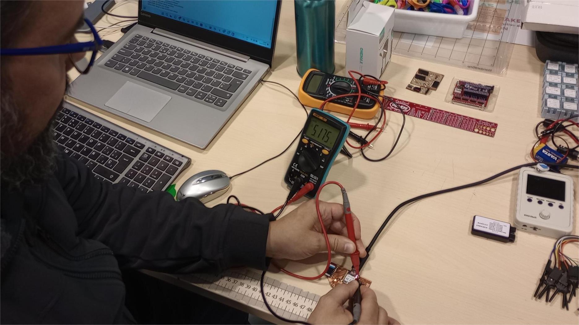
Here I am testing the voltage out pins on the Xiao RP2040 integrated on the Adrianino board.
OSCILLOSCOPE
The oscilloscope I have access to is the DSO Shell from JYE Tech.
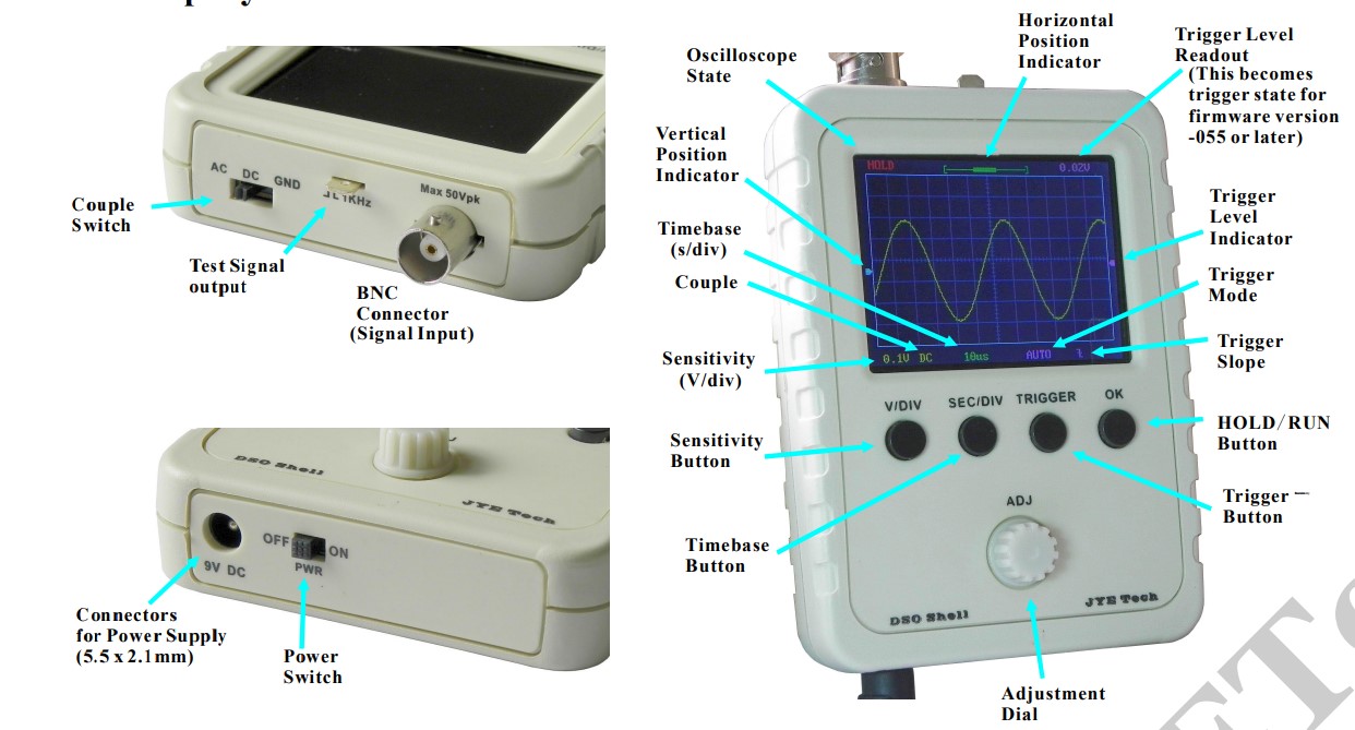
An oscilloscope is used to visualize electrical signals as they varies overtime. It displays the voltage of a signal on the vertical axis and time on the horizontal axis. This allows to observe the waveform of an electrical signal, making it easier to analyse its frequency, amplitude, and shape.
Oscilloscopes are useful to troubleshoot circuits, test components and analyse the signals of electronics systems.
I am using the Adrianino board to measure the voltage output on a pin for a fading LED. I connect the black probe of the oscilloscope to a ground pin and the red touching the active pin of the XIAO RP2040.
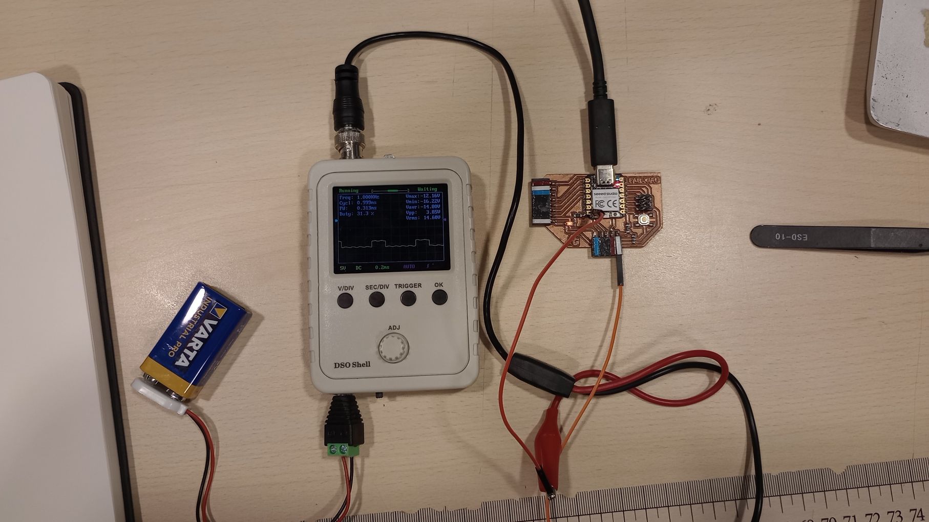
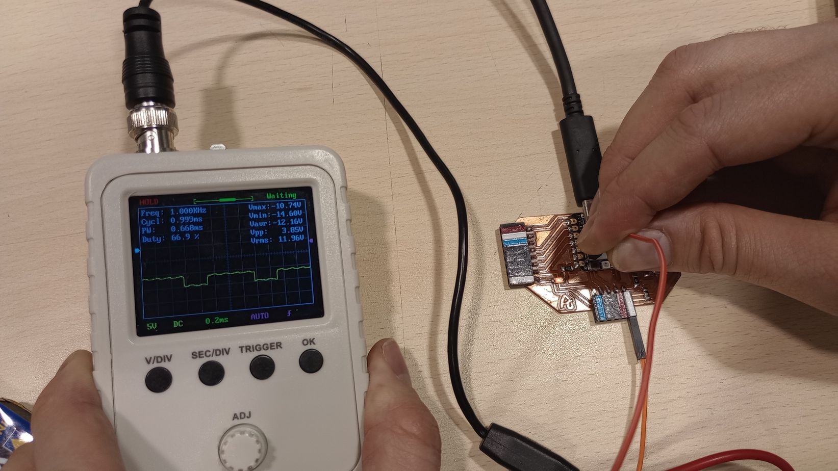
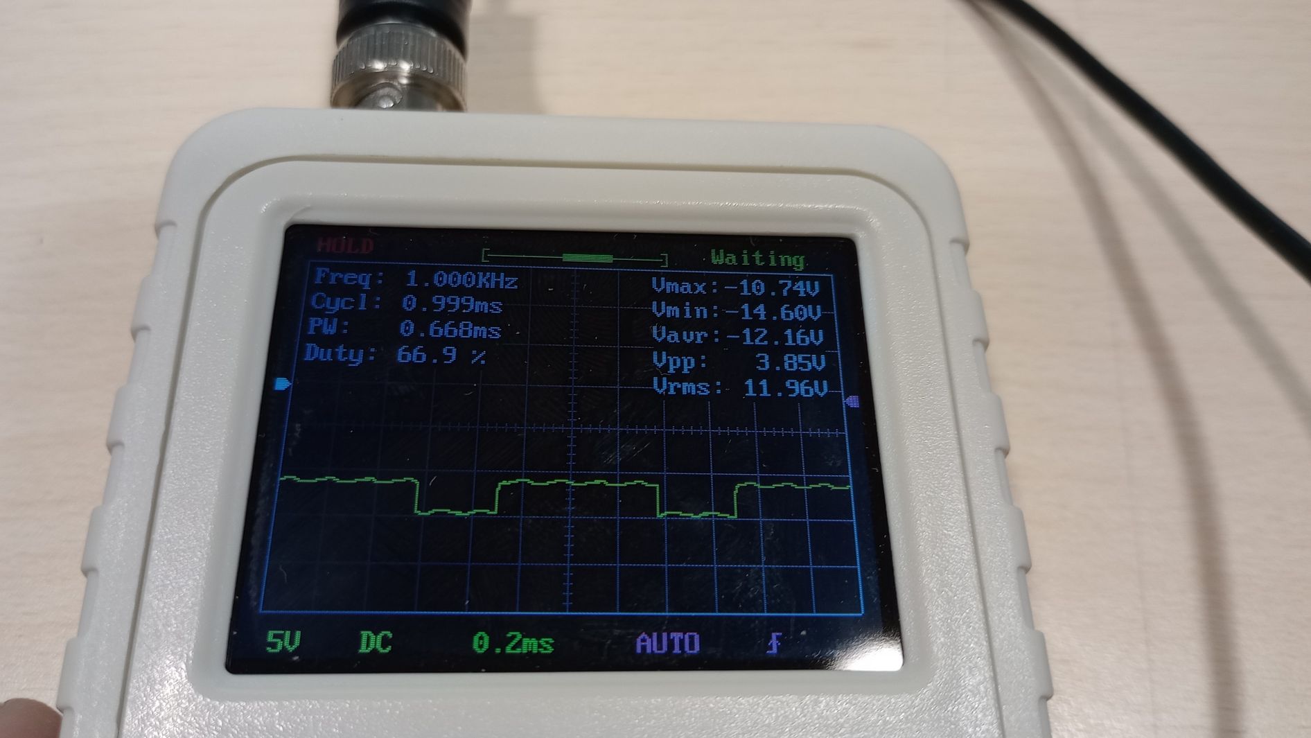
The grid on the display has a 5V scale on the vertical axis and 0.2ms on the horizontal. It shows a rectangular wave with a peak to peak voltage (Vpp) of 3.85V and a cycle of 0.999ms.
The square wave means the voltage on the pin is turning on and off, each fading cycle of the LED lasts 1 second and the voltage measured on the pin is 3.85V.
LOGIC ANALYZER
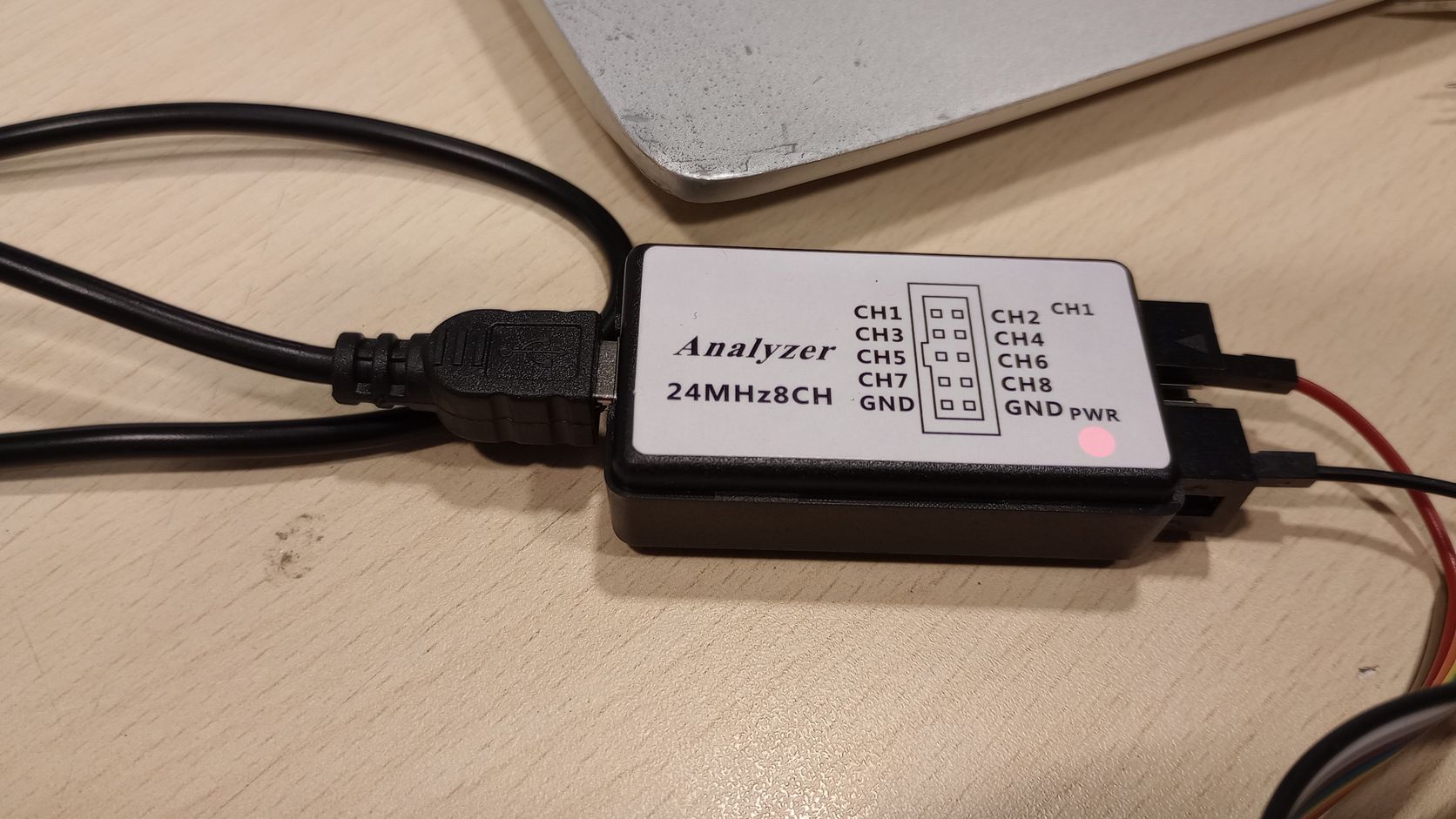
A logic analyzer is a device used to capture and analyze the digital signals in an electronic circuit. It allows you to monitor multiple signals (or "channels") simultaneously. It is used to troubleshoot electronic circuits, to decode and analyse communication protocols like I2C, UART, and for testing and debugging of embedded systems.
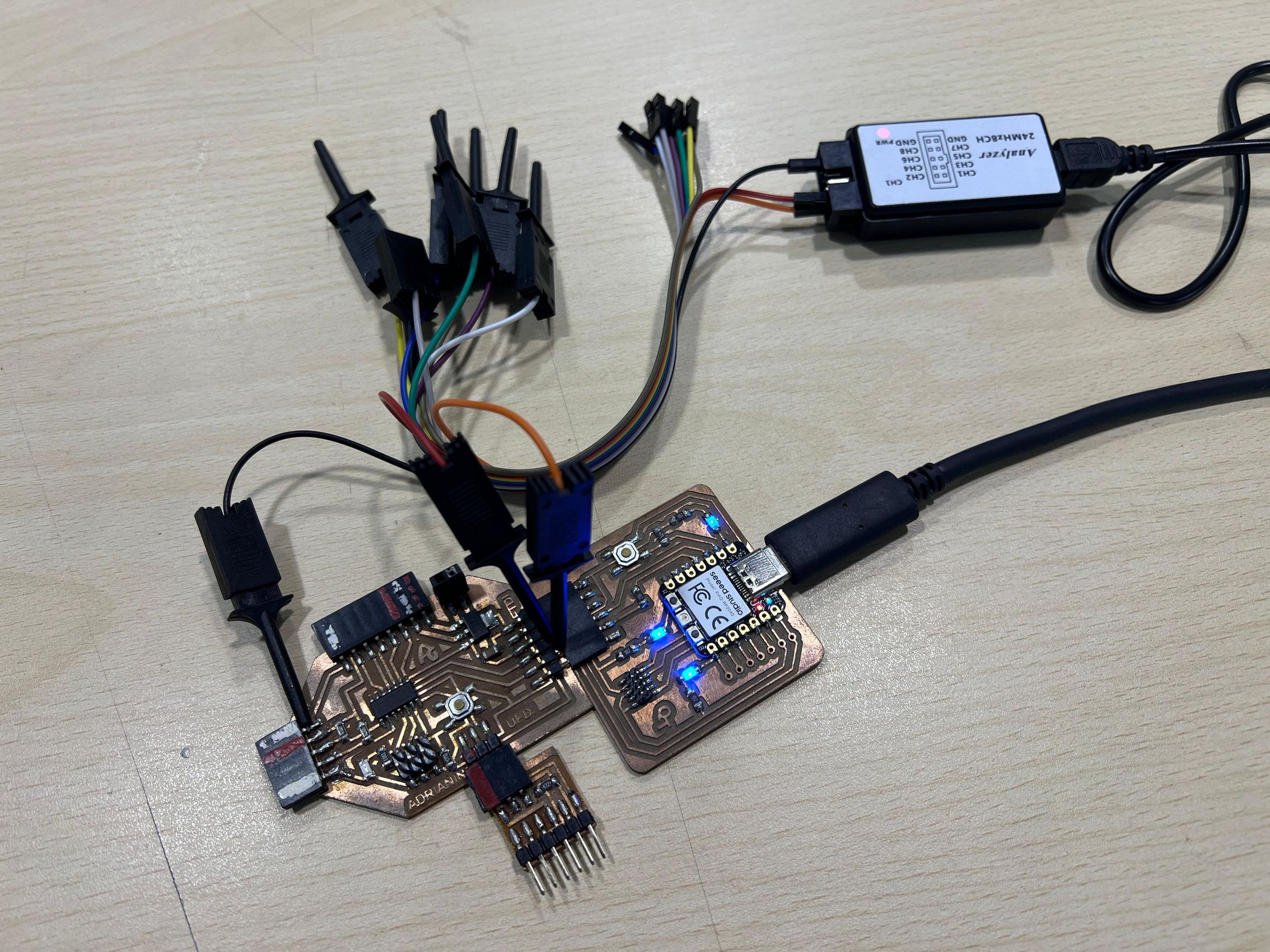
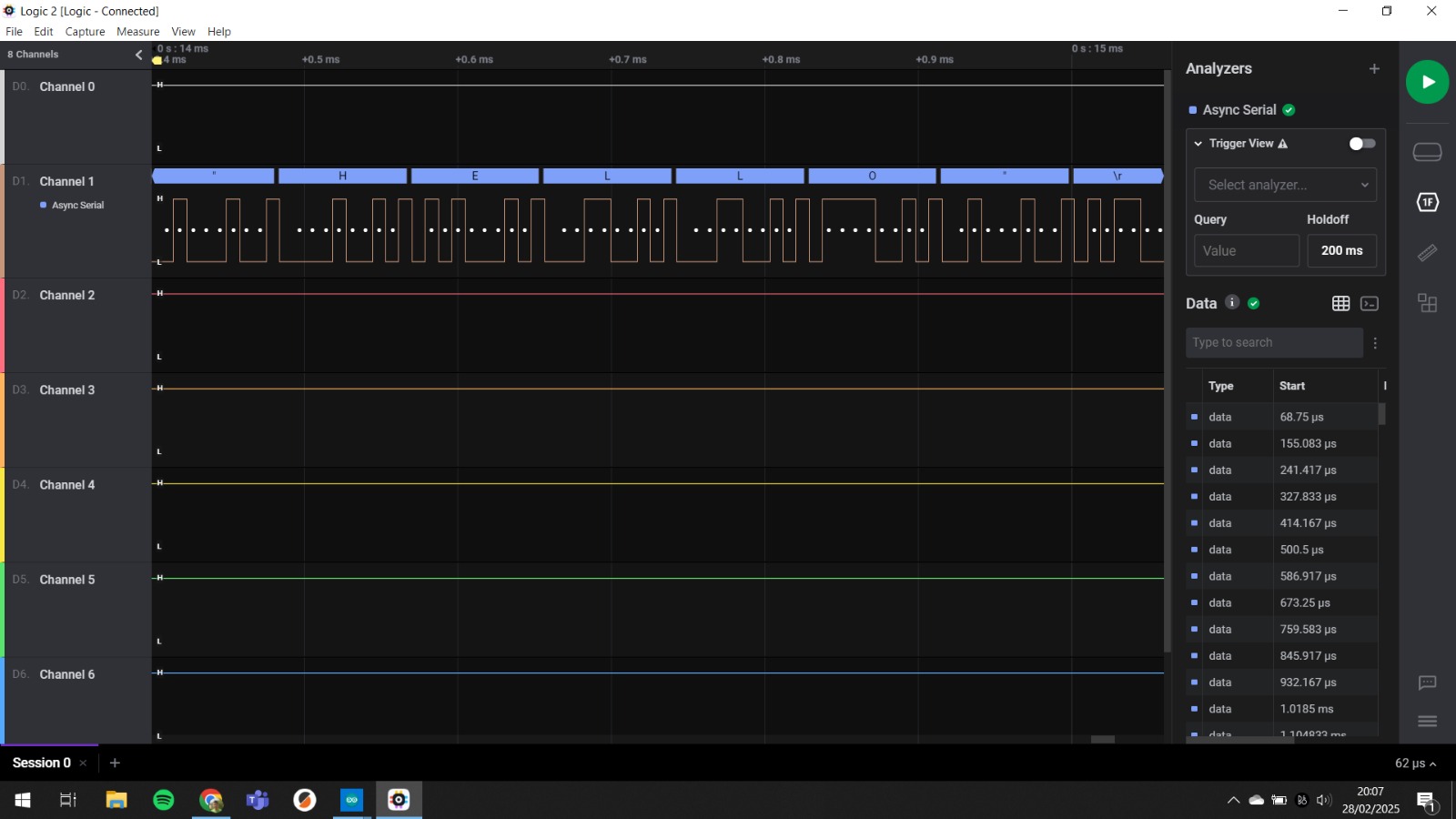
I am using an 8-channel logic analyzer device with the Saleae Logic2 software to decode serial communication.
The board being tested is an Adrianino (ATtiny1624) which is connected to the Quentin-Torres board using the FTDI connection. By connecting the QT to the computer I can have serial communication between the Adrianino and the Arduino IDE.
I connect the analyzer to the laptop via USB cable and to the board using 3 testing clips:
- the ground testing clip to a ground on the board,
- testing clip from channel 0 on the logic analyzer to the Tx header pin on the board
- testing clip from channel 1 on the logic analyzer to the Rx header pin on the board
The Rx pin is used to receive data and the Tx pin is used to transmit data.
Once the physical connections are completed I upload Neil's “tiny412 echo hello-world”
program on Arduino IDE to send and receive information to and from the microcontroller through the Tx and Rx pins.
Next step is to configure Logic2 following the steps in this software documentation. I click the Analyzers panel button and then the + button to add a protocol analyzer. I configure channels 0 and 1 as Async Serial so I can measure serial signals. Async serial communication means any data that is transmitted serially (i.e., one bit at a time). The bit rate (bits/s), or baud rate, will be 115200.
The protocol can be displayed in binary, decimal, hexadecimal, or ASCII. In this case I select ASCII as the encoder standard.
From the serial monitor I type “hello” and the Logic Analyzer records the transmission of data and Logic2 shows a graphical representation of the bits transmitted and the characters as shown in the following screenshot.
Top
INDIVIDUAL ASSIGNMENT: ELECTRONICS DESIGN
For my circuit design project, I am using KiCad 9.0, a powerful tool recommended by FabAcademy. KiCad is an open-source Electronic Design Automation (EDA) software that offers a graphical interface for creating electrical schematics, editing PCB layouts, a 3D viewer, managing libraries, and other features that support the entire electronic circuit design process.
After installing KiCad 9.0, I followed this GitHub repository by Krisjanis Rijnieks to install the updated library of components used by Fab Academy.
Installation of Fab Electronics Library for KiCad
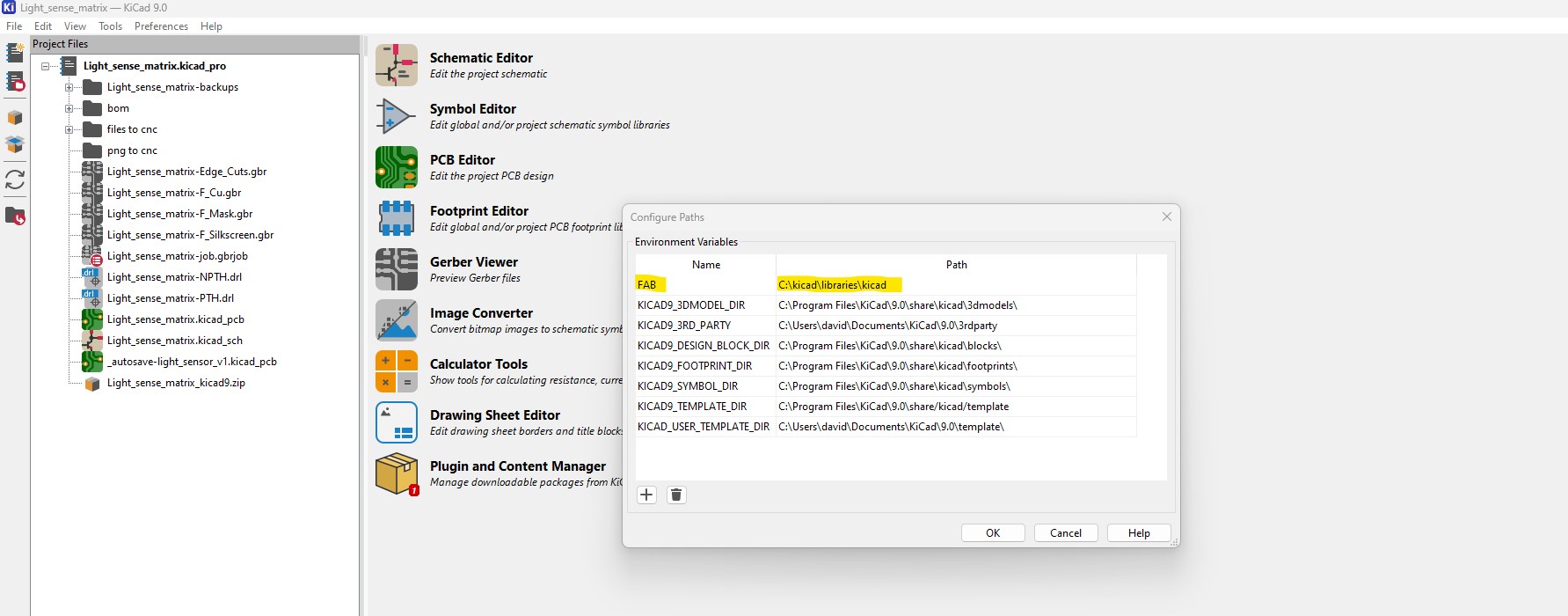
- I downloaded the repository and I renamed adownload this repository to “fab”.
- I saved the directory in C:/kicad/libraries/kicad.
- Open KiCad9.0.
- In "Preferences / Configure Paths" I added a new environment variable "fab" that points to location of the fab library on my drive, C:/kicad/libraries/kicad. This is needed for the 3D models to load correctly.
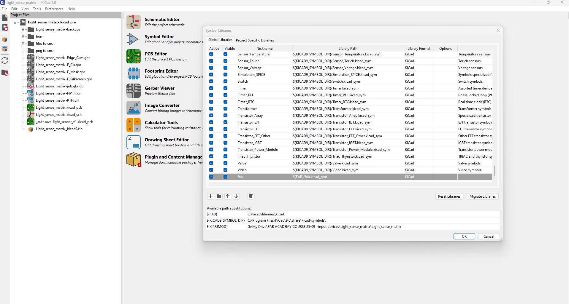
- In "Preferences / Manage Symbol Libraries" I added fab.kicad_sym as symbol library.
- In "Preferences / Manage Footprint Libraries" I added fab.pretty as footprint library.
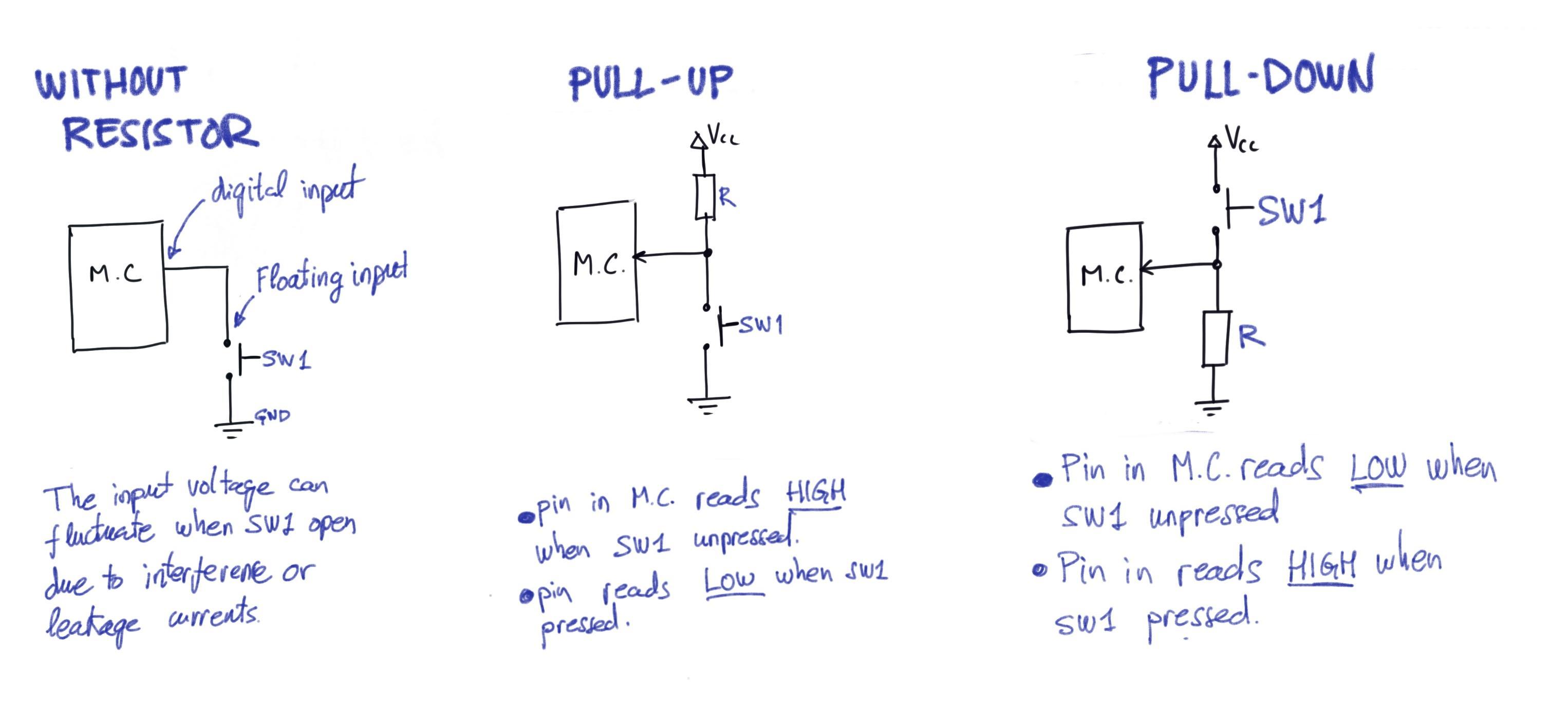
My plan for completing the assignment is to design a circuit that incorporates external pull-down and pull-up resistors to control two separate LEDs. It must be noted that microcontrollers usually include pull-up internal resistors that can be activated with code so the external ones are not really needed in this case.
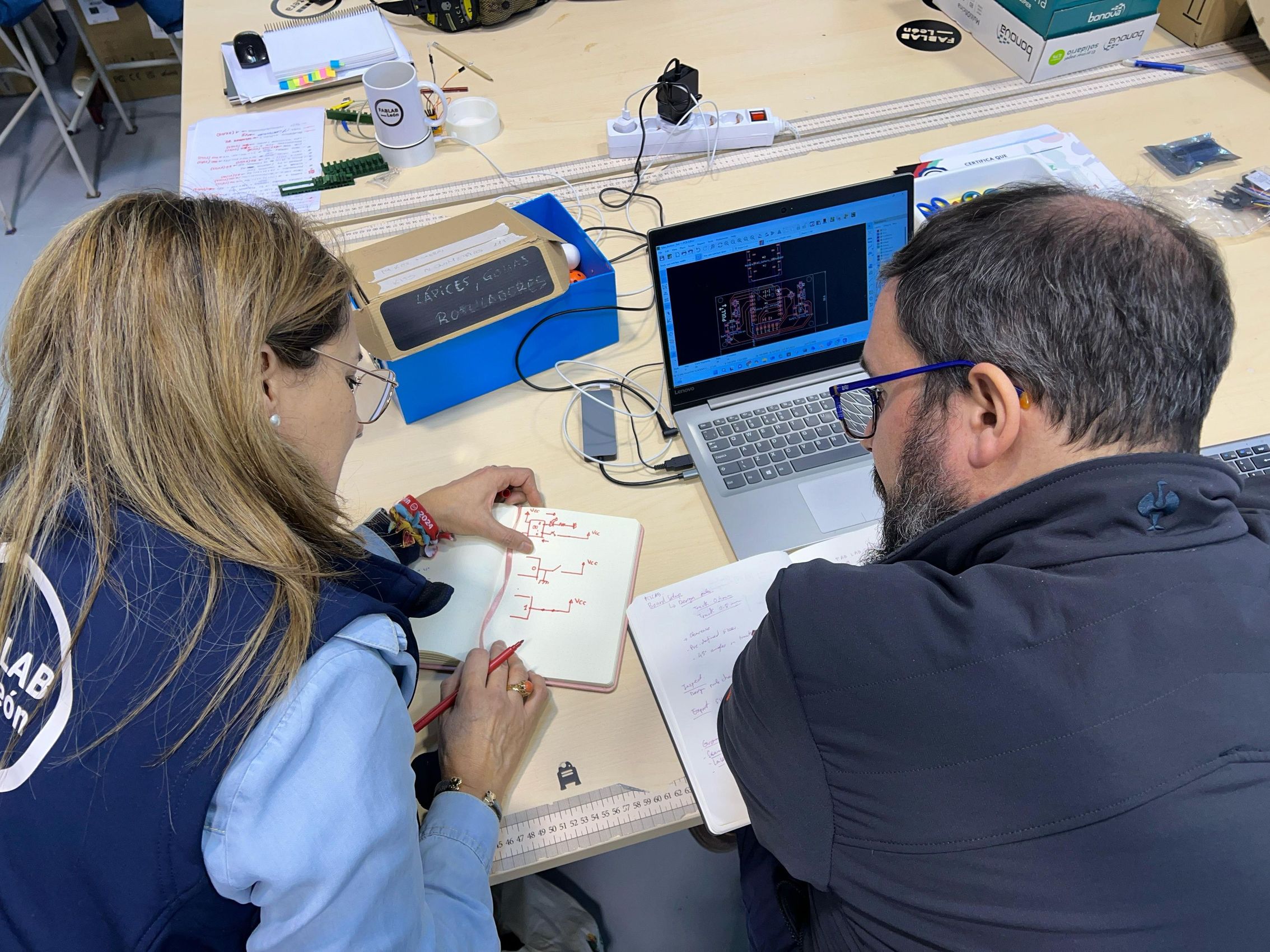

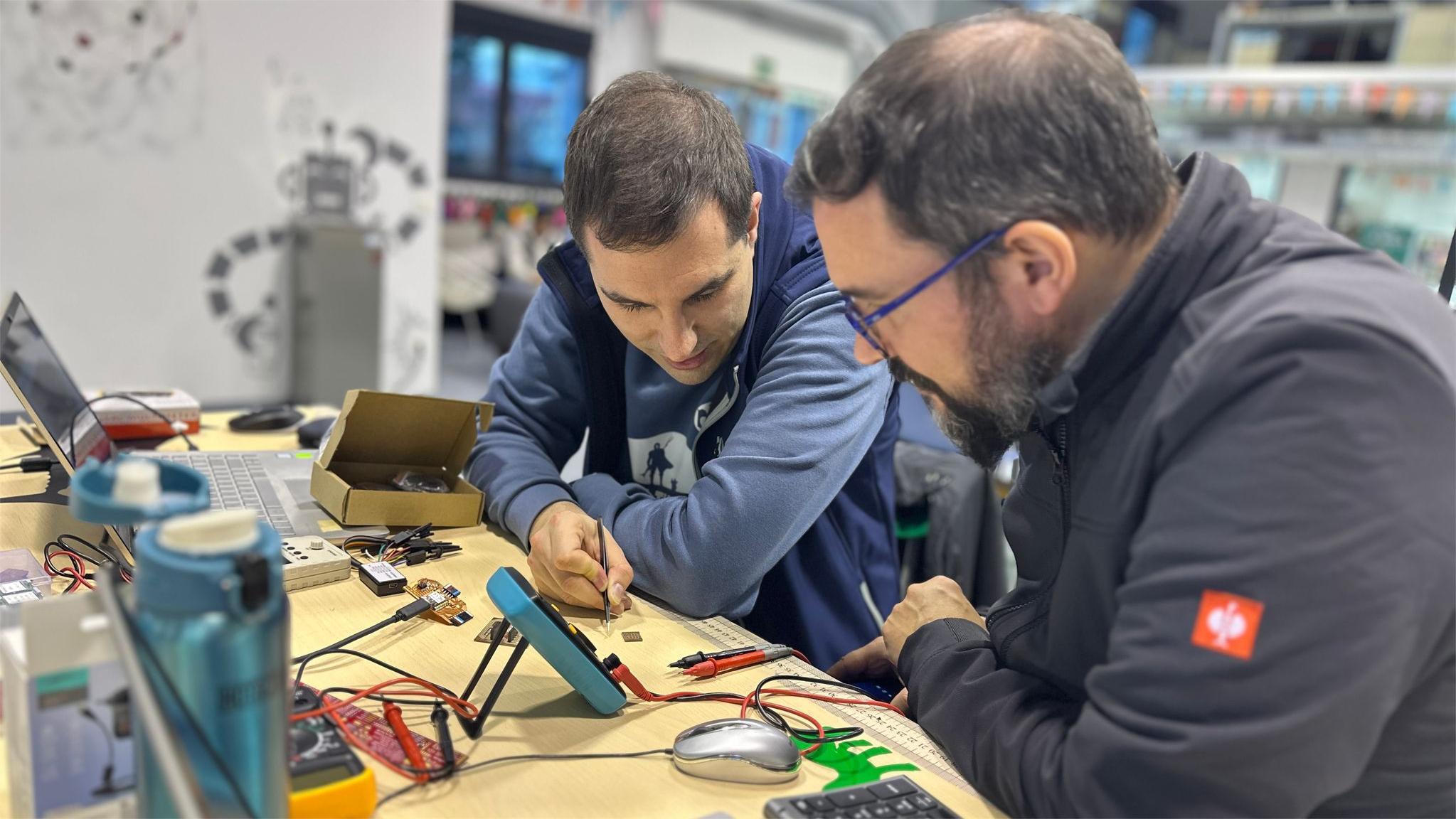
Fortunately I spent a productive day at Fab Lab León, where Nuria, Adrián, and Pablo assisted me with my assignments. They helped me learn how to use testing tools, use an EDA tool, and understand pull-up and pull-down configurations.
When a switch is connected to a microcontroller pin and ground, it creates a "floating input" when the switch is open. This can cause the voltage readings on the pin to fluctuate, which results in unpredictable behavior due to noise interference.
Pull-up and pull-down circuits are implemented to ensure a known voltage level (either HIGH or LOW) on a signal line when it's not driven by another component.
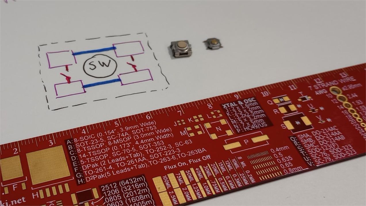
Thanks to Nuria's clear explanation and my own diagram with notes, I now have a solid understanding of the importance of using pull-up and pull-down resistors. These components are essential for ensuring stable readings from digital inputs in electronics.
The components I am using for the design and eventual fabrication are SMD (surface-mounted devices), which are placed directly on the surface of the PCB. This is different from the through-hole system, which requires drilling holes to insert the legs of the components.
It is also important to know the type of SMD package and specification of components that I am using as the size of an SMD component impacts the power handling and assembly of the PCB. The SMD size will also determine the footprint and layout of components and tracks on the PCB.
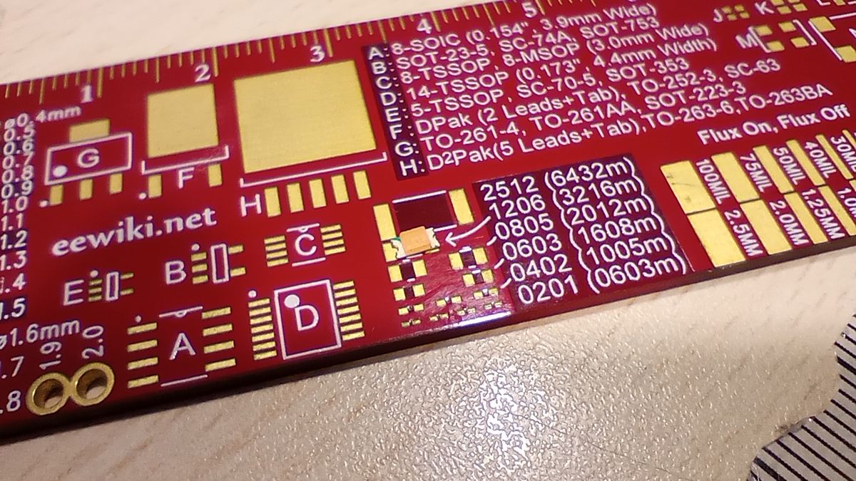
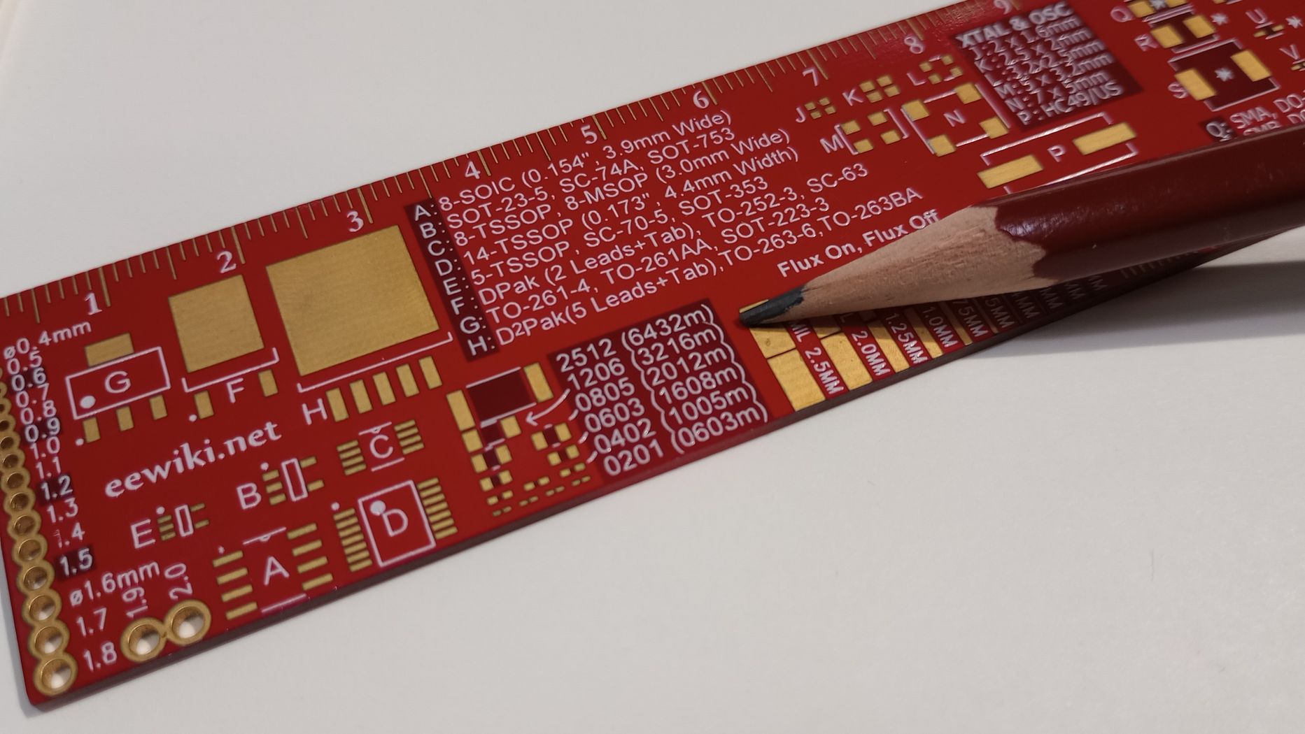
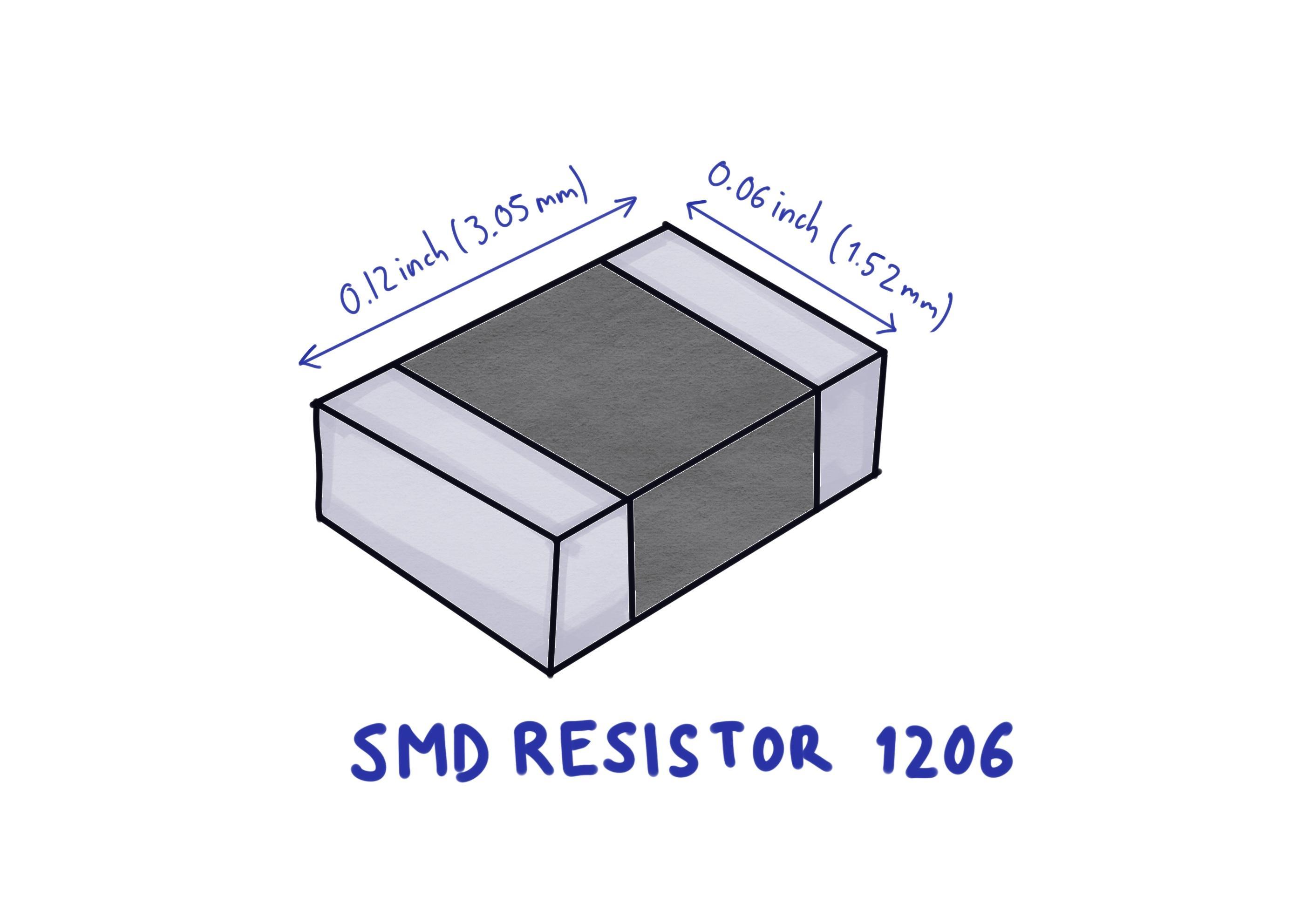
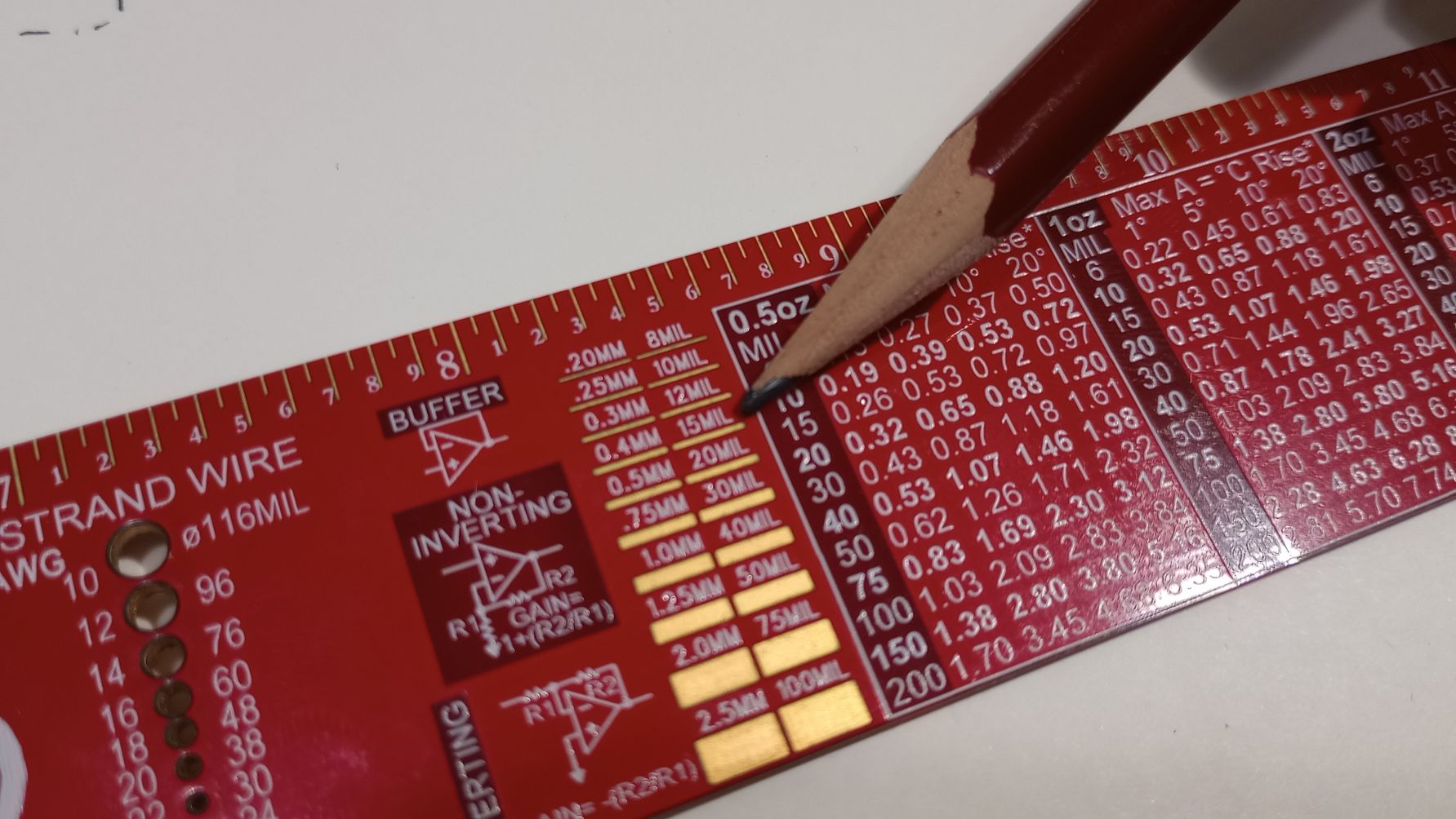
For this assignment I am using SMD components 1206 as they are available in Fab Lab León. Smaller components will be also quite difficult to solder by hand.
This photo of the Digikey PCB ruler shows the different SMD resistor sizes and the drawing shows the dimensions of SMD1206 Resistor.
USING EDA TOOL FOR ELECTRONICS DESIGN
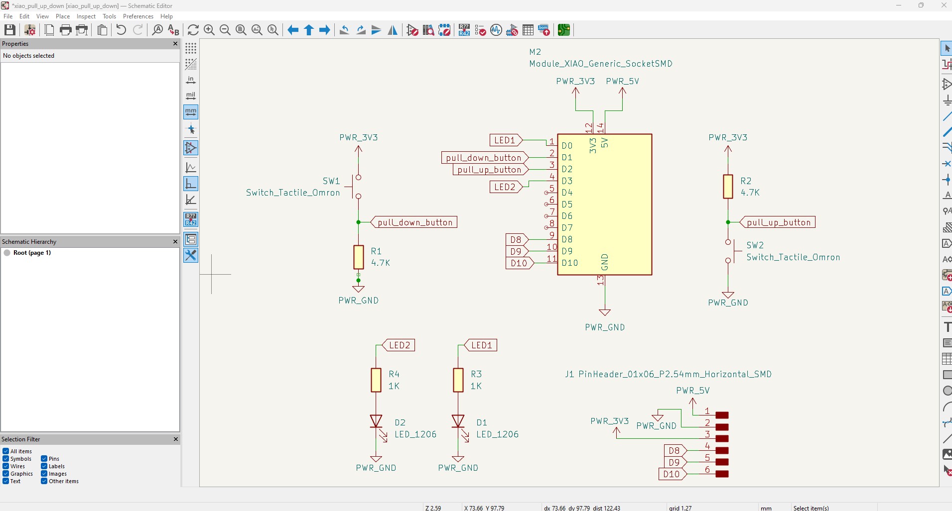
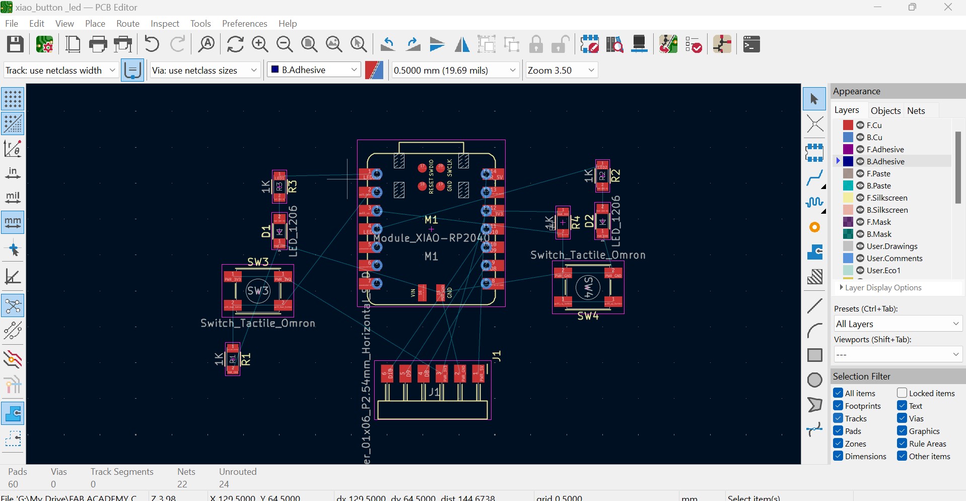
I start creating a new project in KiCad and use the Schematic Editor to create a initial version of the circuit. From the fab library I place a Xiao RP2040, tactile switches, resistors and LEDs to create a pull-down and a pull-up circuit.
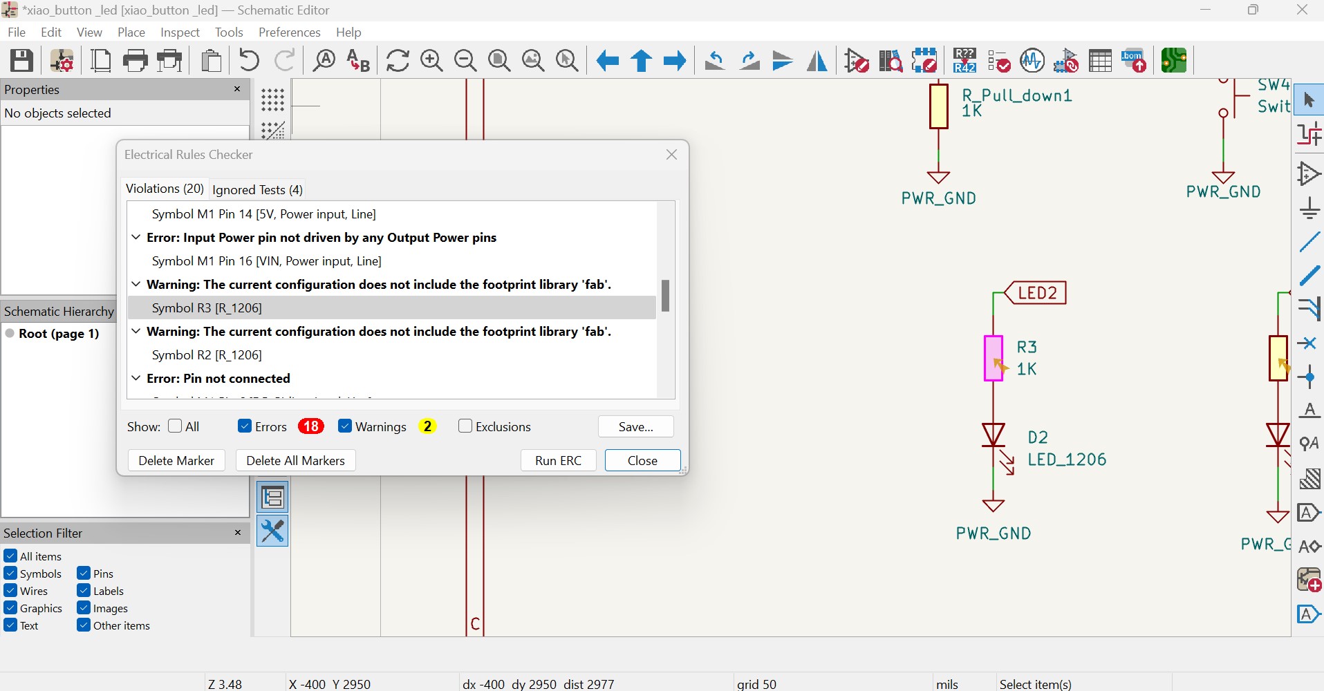
After completing the initial version of the chematic, I ran the Electrical Rules Checker (ERC) and encountered several errors and warnings. It appears there is an issue with the footprint library. Although this does not affect the schematic itself, I will need to address it in order to generate the PCB layout.
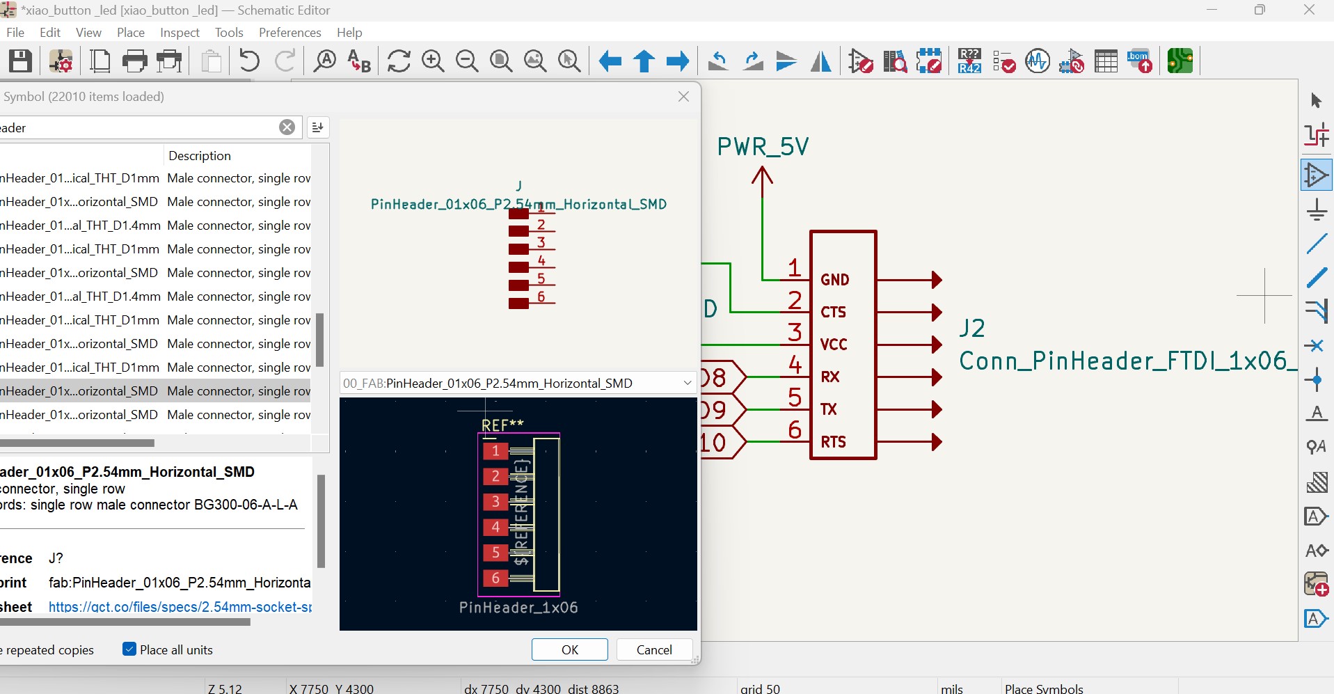
I make other changes to the circuit; for example, Adrián recommended using horizontal pin header connector instead of the vertical one I had originally placed.
I continue working on the schematic. Initially, I began by connecting components with wires, but I switched to connecting pins using labels because I believe this makes the circuit tidier and easier to read. I also managed to solve the issue with the footprint library; the problem was that Config Path y used for the fab library was not correct.
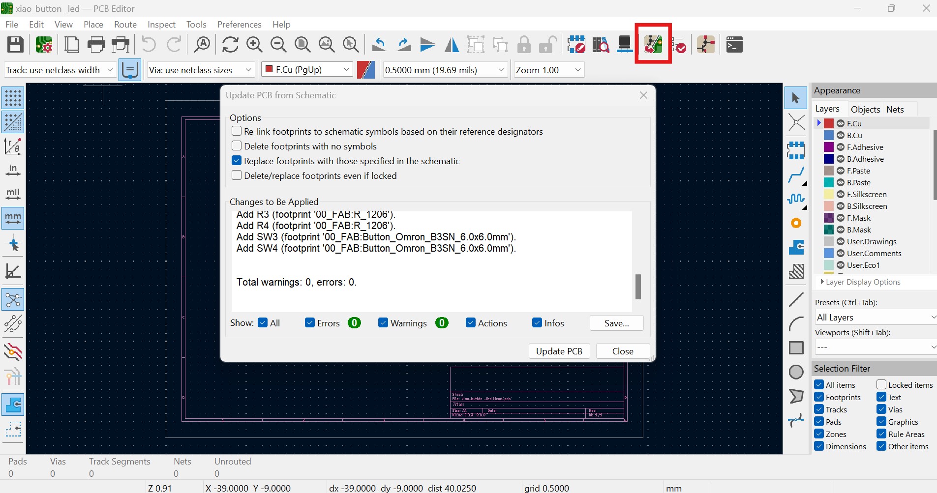
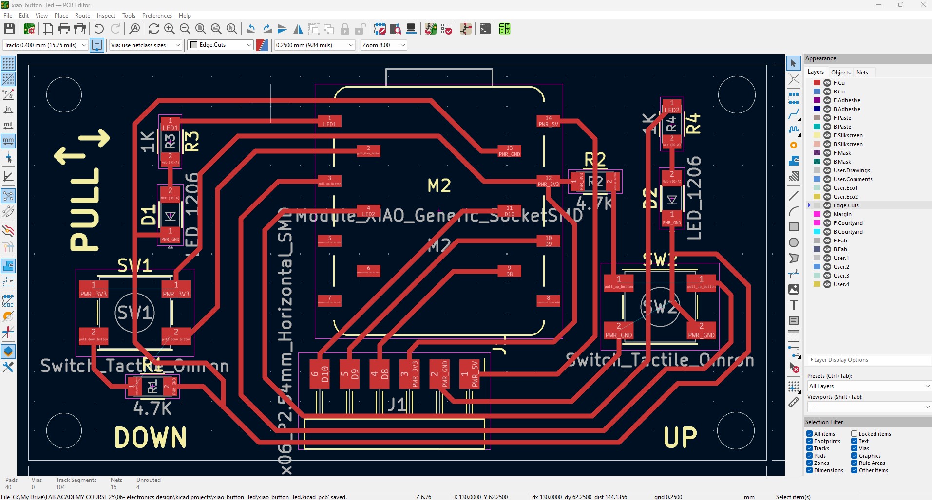
After running the ERC again and disregarding errors realated to unconnected pins on the microcontroller I moved on to the PCB Editor. I use Update PCB from Schematic option to bring in the footprints of the components and connections I have defined in the schematic.
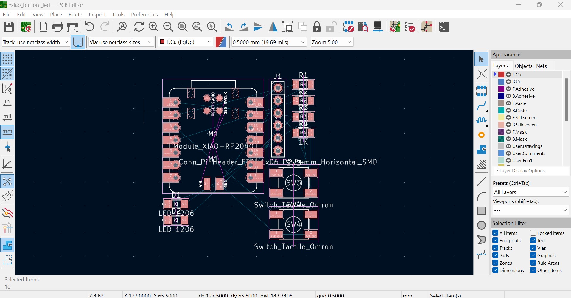
It is necessary to rearrange the components automatically placed on the PCB Editor to achieve an efficient layout of the PCB that can be manufactured.
I manually arrange the components keeping the pull-down configuration on the left and the pull-up on the right of the microcontroller.
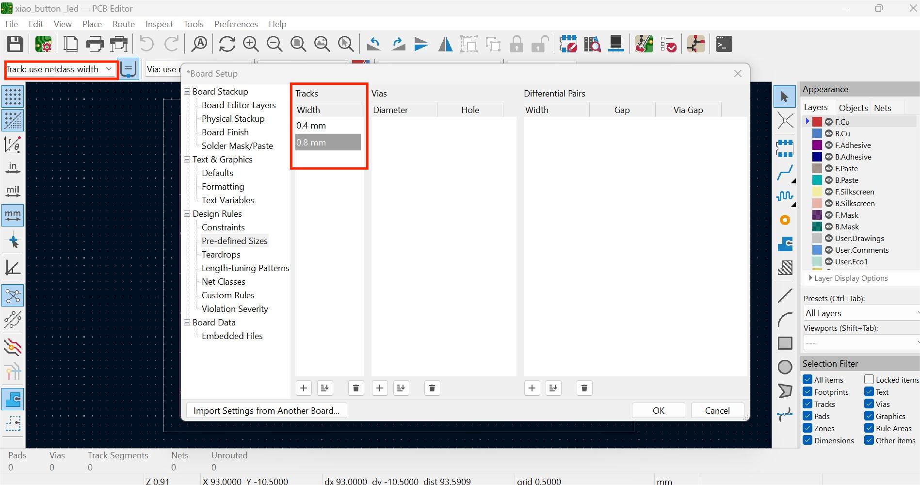
Before routing in the KiCad PCB Editor, I define the track sizes as 0.4mm and 0.8mm.
When adding the tracks I try to avoid right angle corners, I keep the tracks spaced out, and the I run some tracks under the Xiao or between the pads of other components.
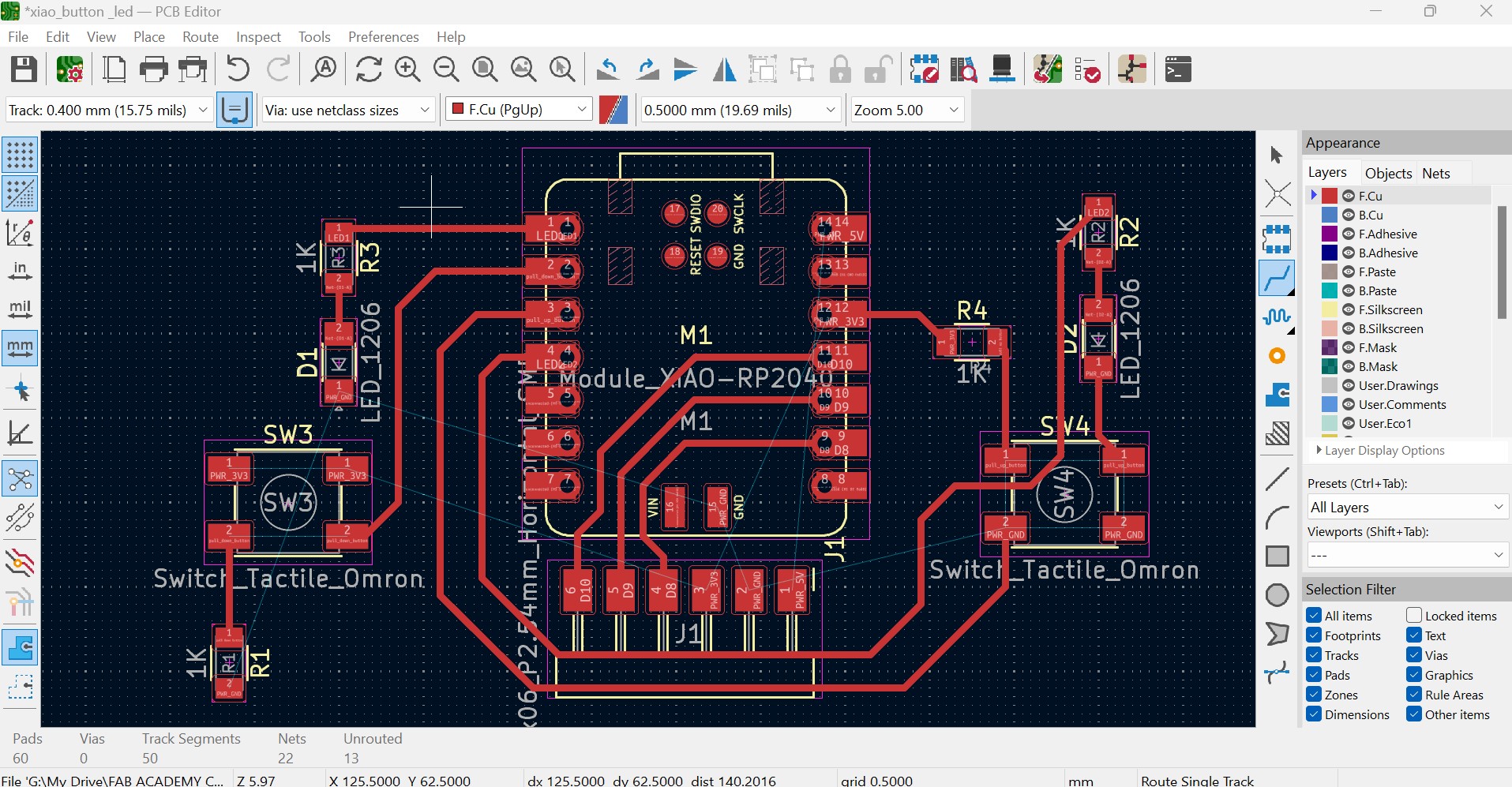
I initially started using the Xiao RP2040, but since I didn't want to solder the microcontroller directly onto the board, I switched to a Xiao mounted on vertical SMD sockets. This change required me to update the schematic and remove the old component from the PCB editor.
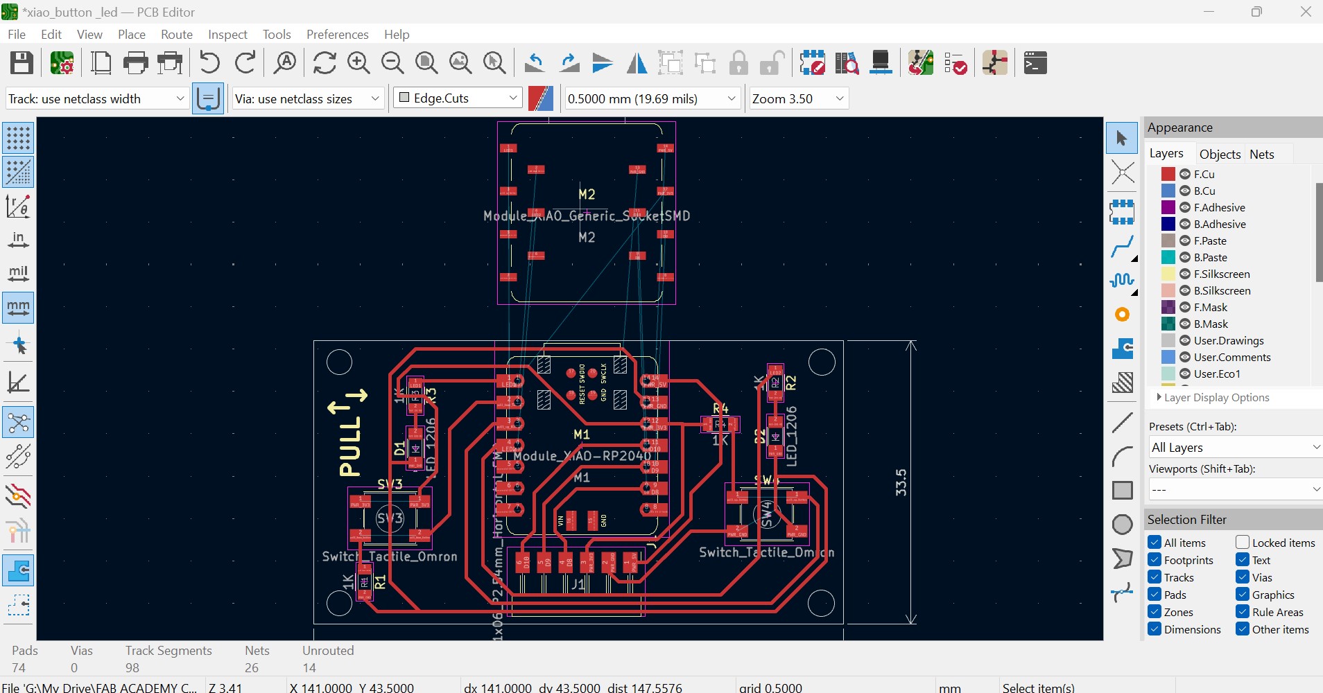
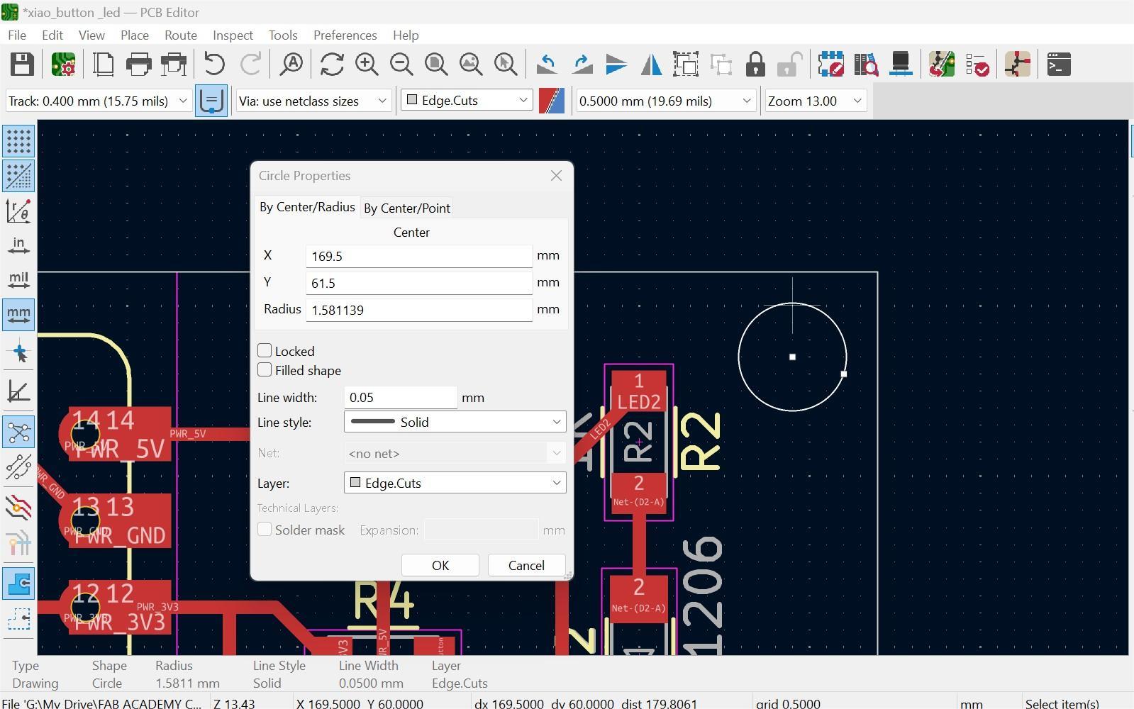
After finalizing the PCB layout, I draw the board edges and 3mm diameter mounting holes on the layer Edge.Cuts. I also add text using the layer F.Silkscreen.
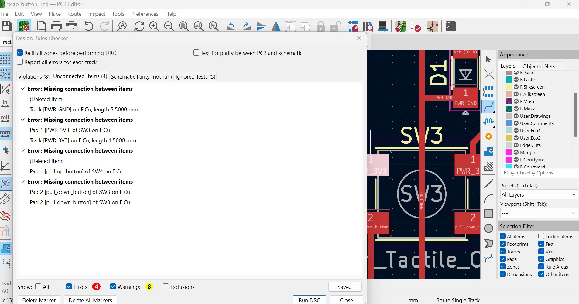
After running the Design rules checker I realize I need to fix some unconnected tracks. The buttons also trigger a “missing connections” error but I ignore it as the connections are already done internally in the button.
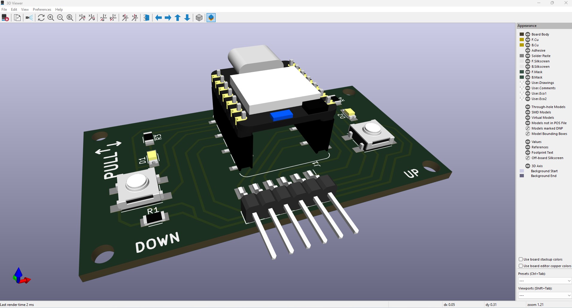
The next screenshots show the completed PCB design and the 3D view of the board.
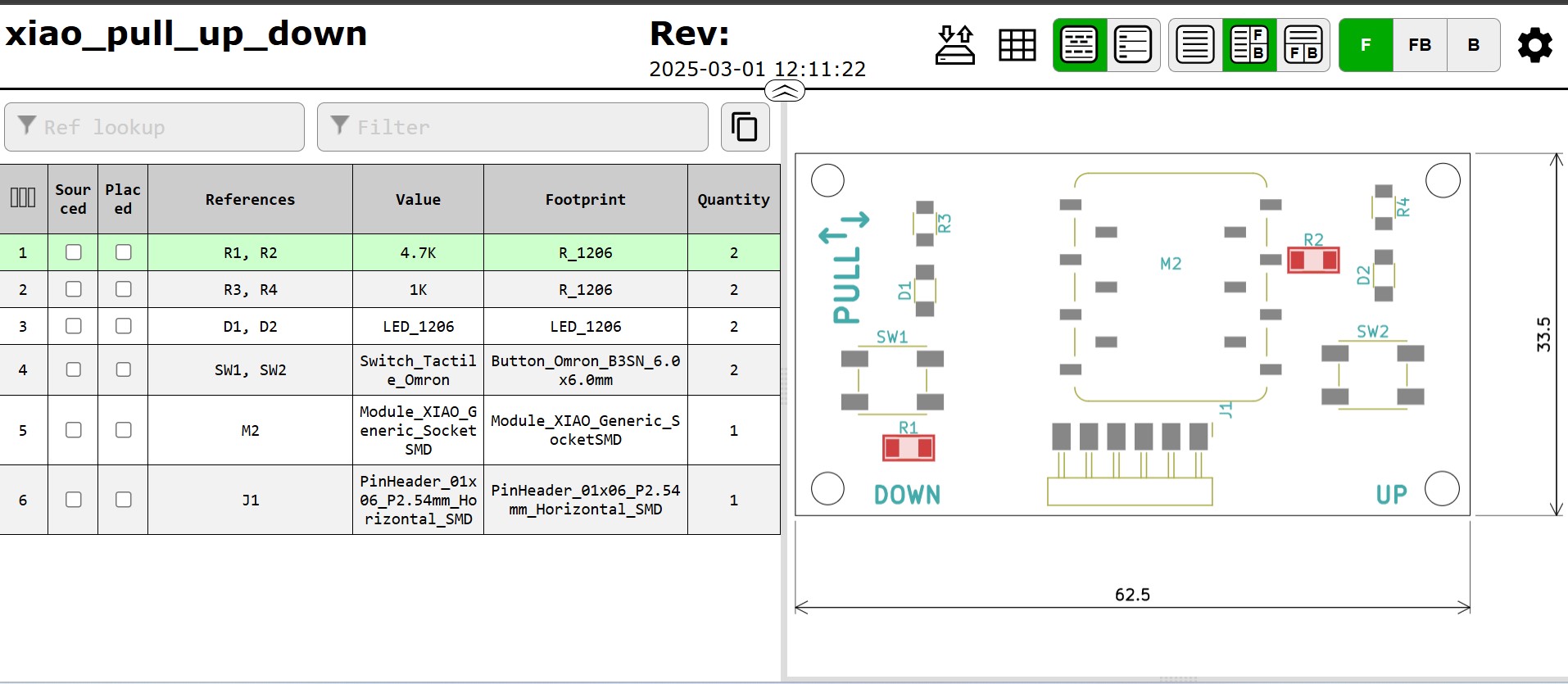
Additionally, I install a plugin (Interactive HTML BOM) to generate a bill of materials that is interactive and can be opened on the browser.
CIRCUIT SIMULATION
To check the circuit will work with a program I decide to create a Wokwi simulation. Since the Xiao RP2040 is not available I use the Raspberry Pico which uses the same chip.
I had to take into account that in the pull-up circuit, when the blue button is pressed the signal in the input is LOW, what sends a HIGH to turn on the blue LED.
Link to simulation in Wokwi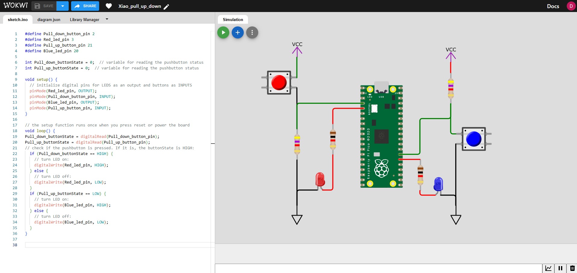
USEFUL LINKS AND RESOURCES
- JYE Tech website. Handheld, portable, digital DIY oscilloscopes and kits: link
- Sparkfun website. How to Use an Oscilloscope: link
- Techtronix website. Oscilloscope Basics: Waveforms, Graph, & Measurement Reading (tecktronix): link
- Using Logic software from Saleae (for Logic analyzers): link
- KiCad components library GitHub repository by Krisjanis Rijnieks: link
- Digikey PCB ruler: link
- Adrianino board documentation: link
FILES
Kicad project Xiao Pull Up & Down board: xiao_pull_up_down.zip
Program for Wokwi simulation: xiao_pull_up_down_code.ino
Top