week 8. electronic production
This Week i started by milling PCBs
In our group assignment, we tested our PCB-Mill. Due to the fact, that i was overseas for a Conference I was just Responsible for The Website. So Crossreading, the Content and also Adding it to the Site and Pushing everything to our Internal Git.
HelloBoard
To get a bit familiar with our Mill and smd soldering, i milled a testboard.
Gerber Files
First thing you need for our PCB-mill are the Gerber files. We need the Front, the Cutout(Edge-cut) and the Drill files:
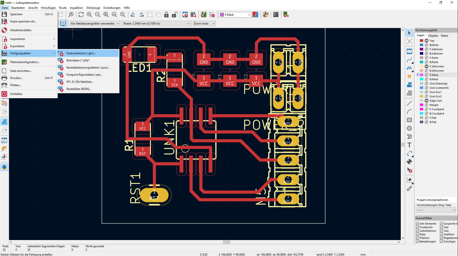
After open KiCad and the Board file, click File -> Fabrication Outputs -> Gerbers
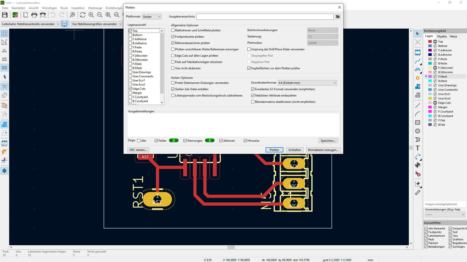
Select Top and Edgecuts and hit plot. After that click on generate drill files
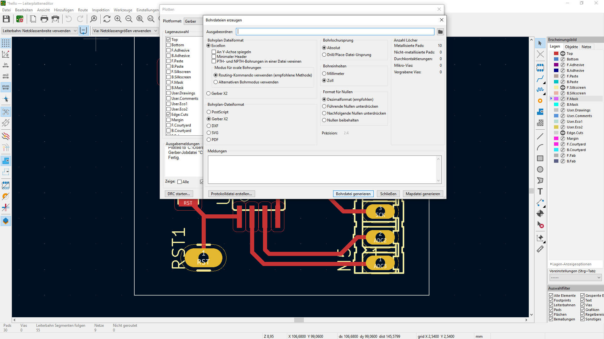
Click on generate drill file. Now our gerber and drillfiles should be in the Project folder
Milling the Board
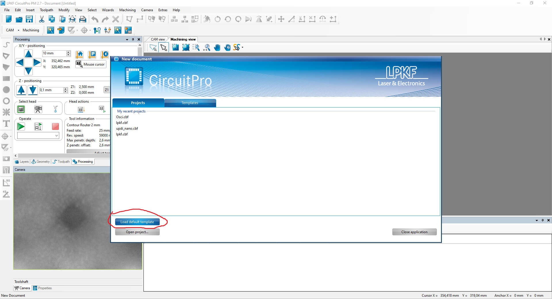
I opened CircuitPro and loaded the default template
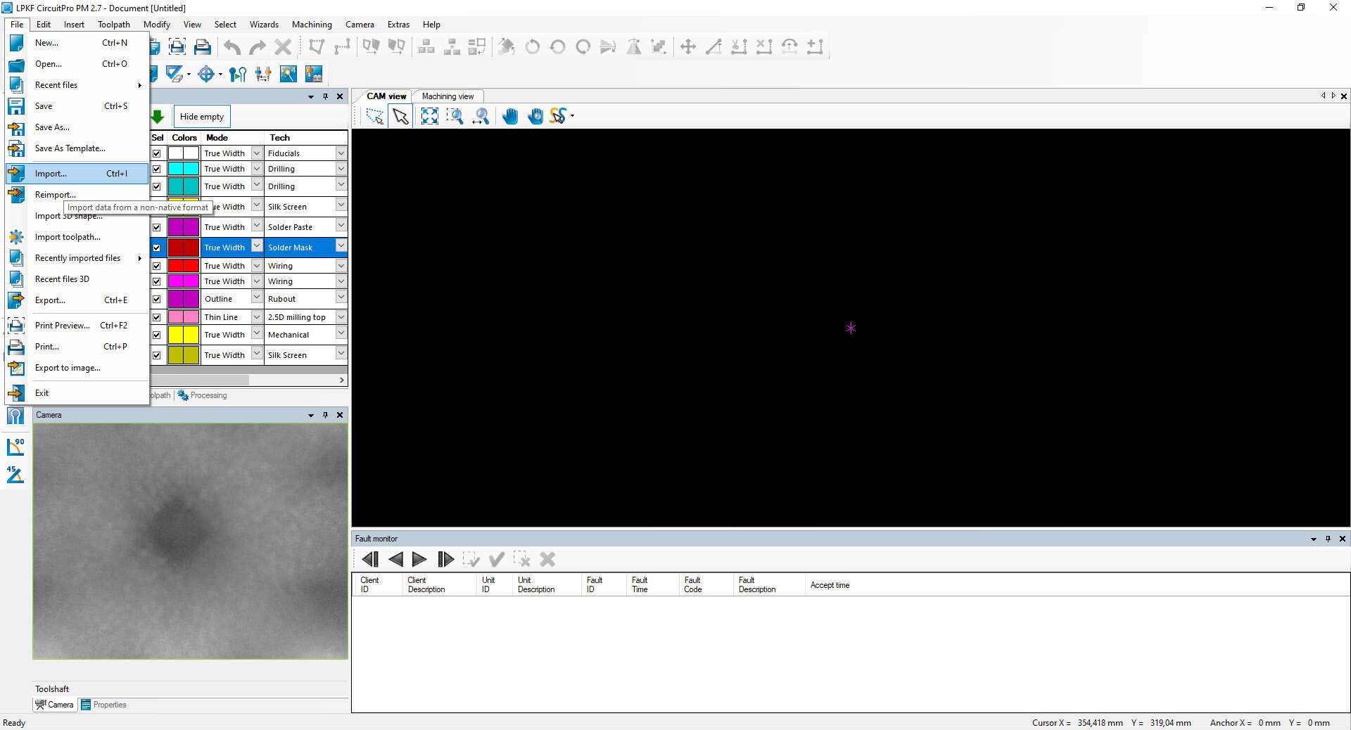
clicked on file -> import
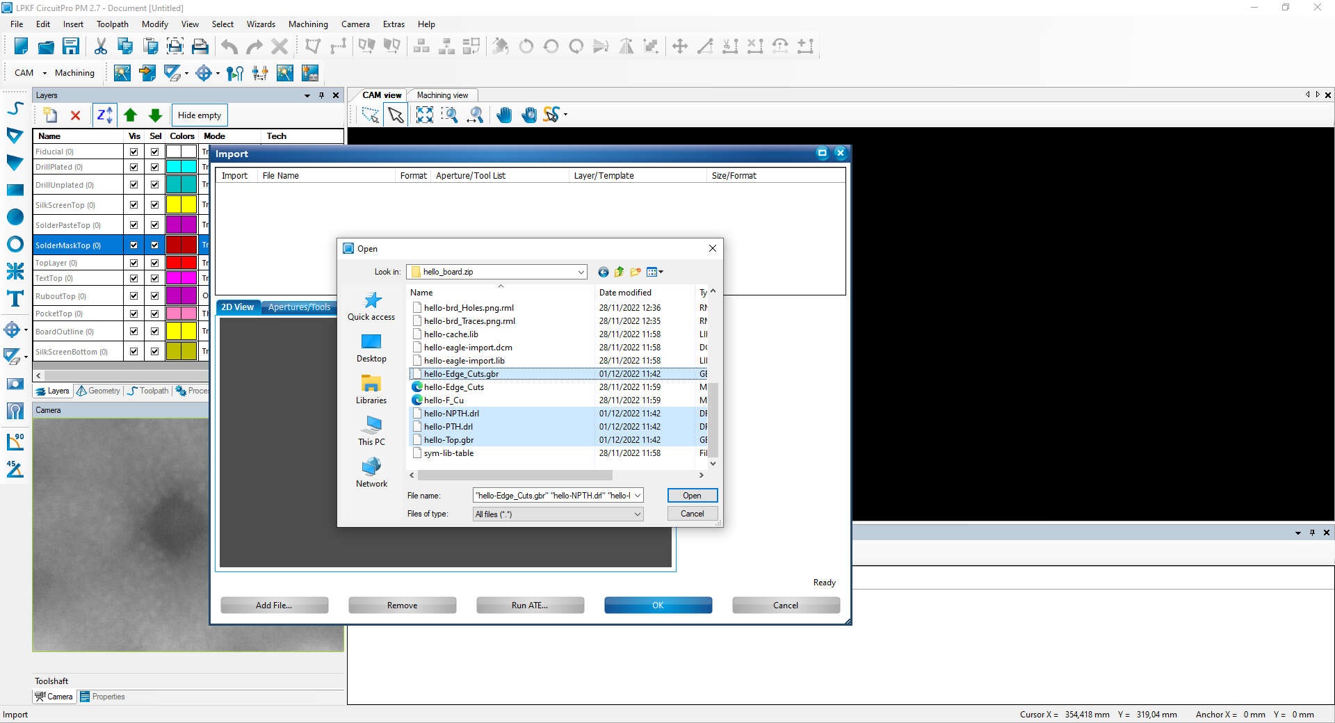
And Import hello-Edge_Cuts.gbr , hello-Top.gbr and hello-PTH.drl
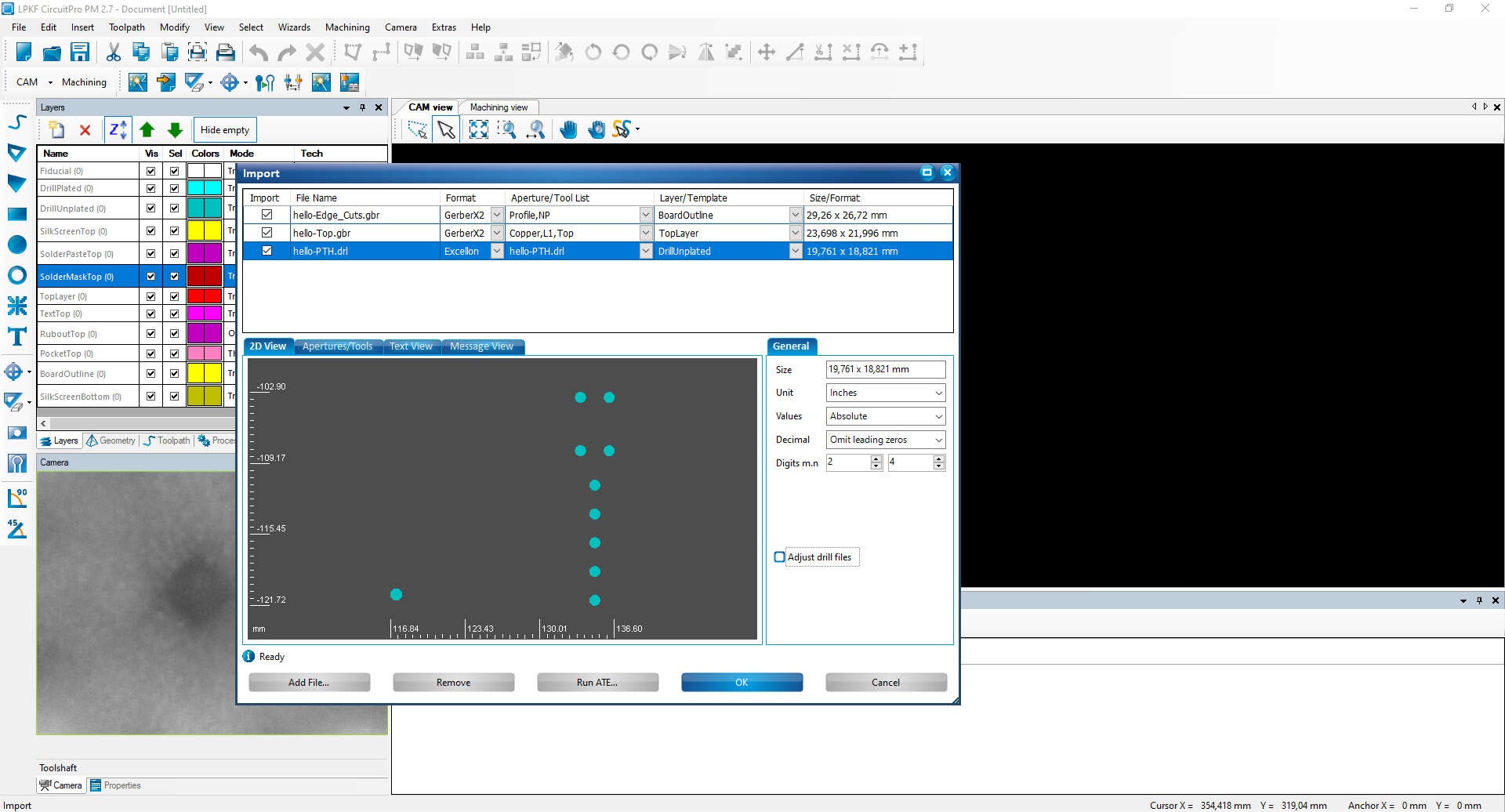
click OK
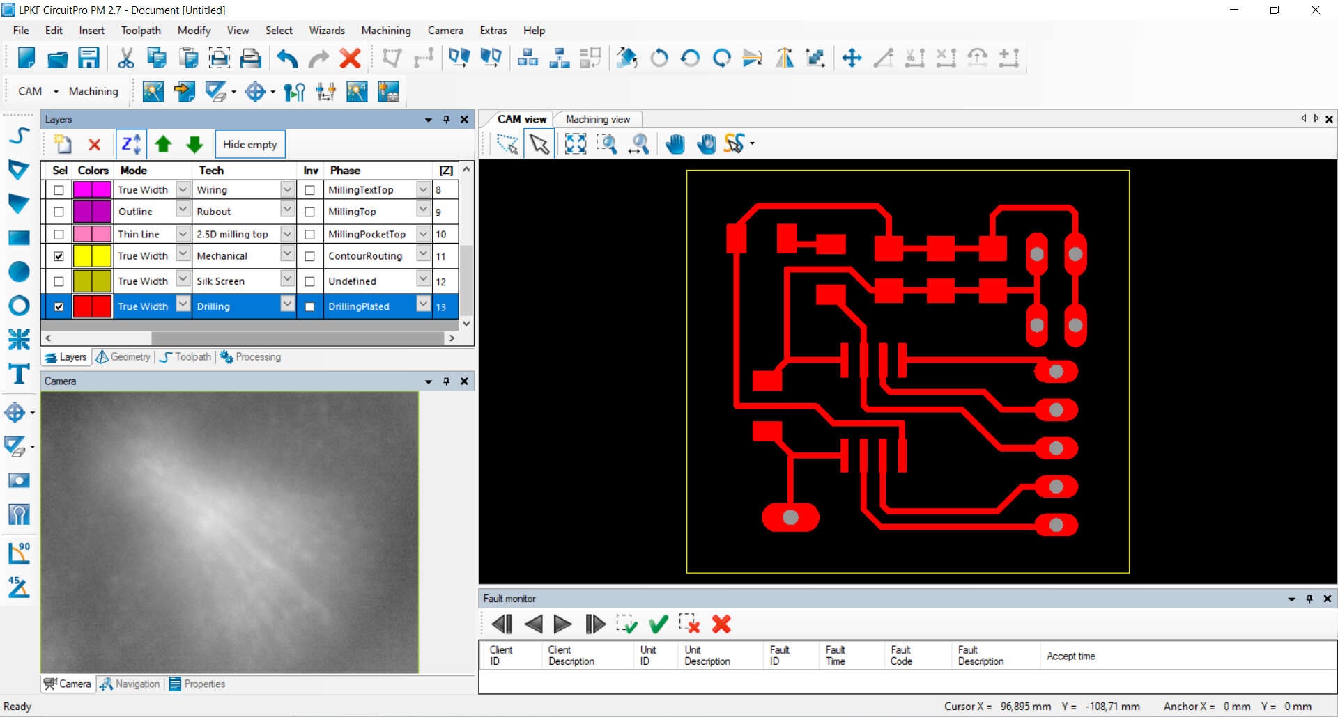
Make sure, that at the drilljob "tech=drilling" and "Phase=DrullingPlated" is selected.
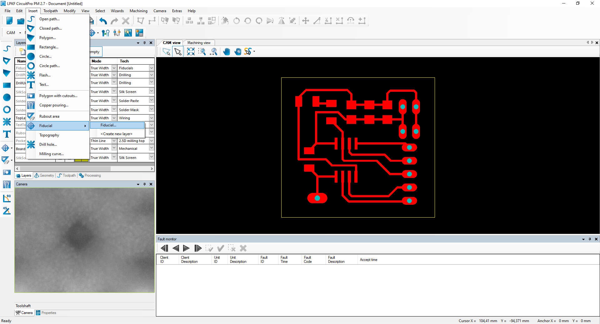
Now I added the Fiducials. Fiducials are holes for registration. They are used to locate the boards position and rotation, if the machine shuted down and you want to proceed with the current board or if you want to mill two sided. for that click on insert->Fiducal->Fiducal
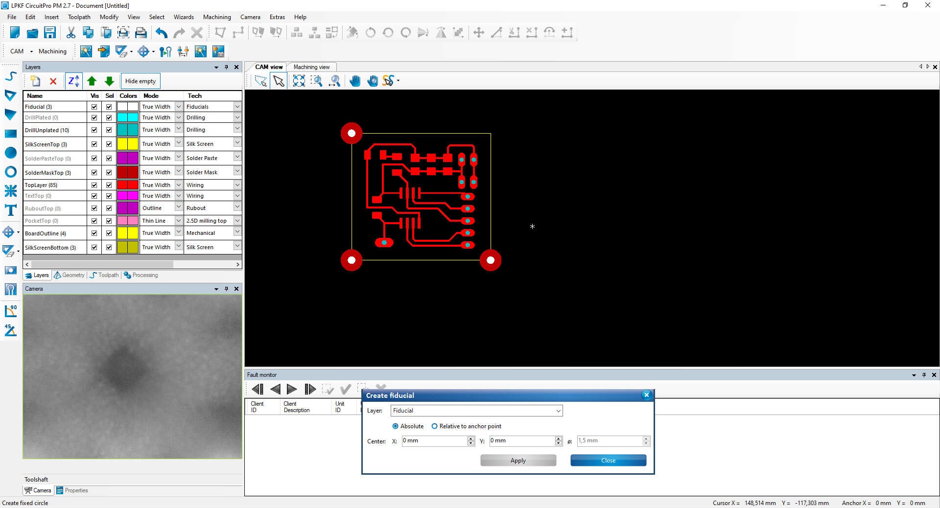
Click onto three edges of your board. Fiducals are used for positionrefference. After that, click on close
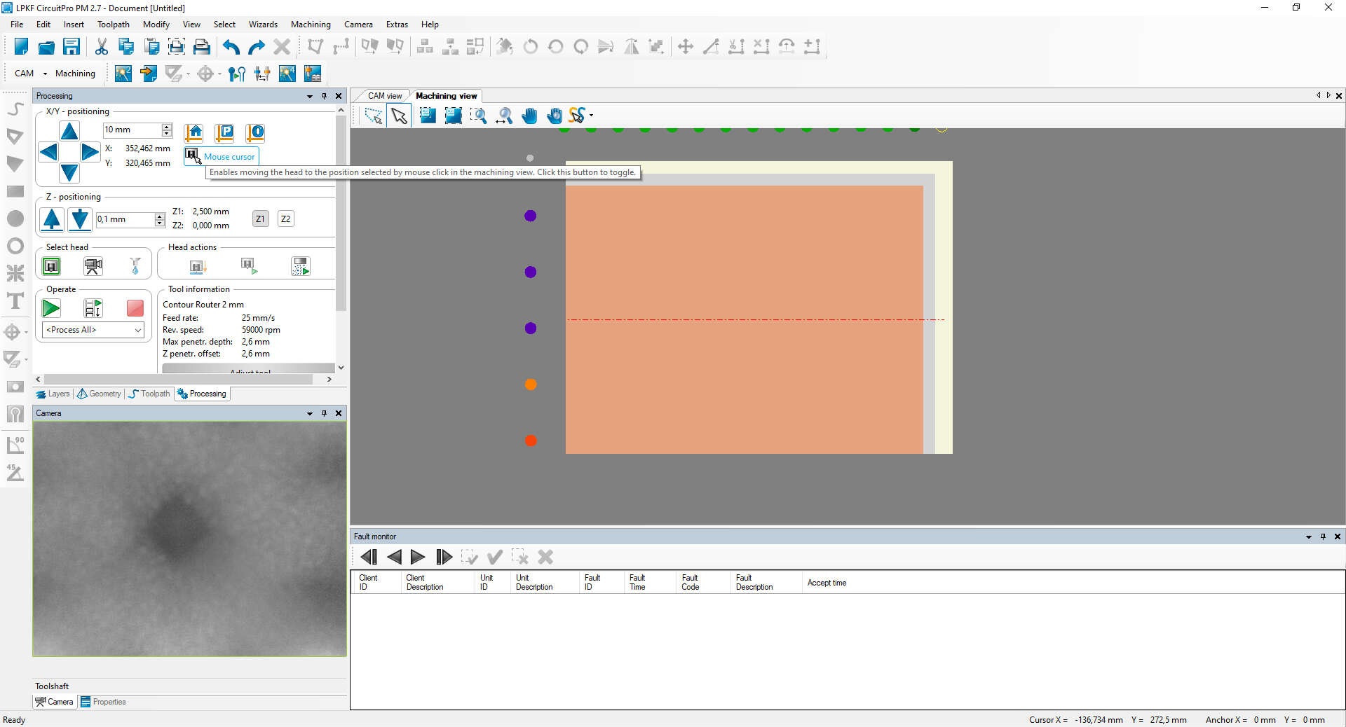
Next Step is to mount the PCB Material onto the mill as shown on the next pic. When mounted we click on Mouse cursor in the X/Y - positioning Area. you can move the mill head my clicking in the machining area inside the programm
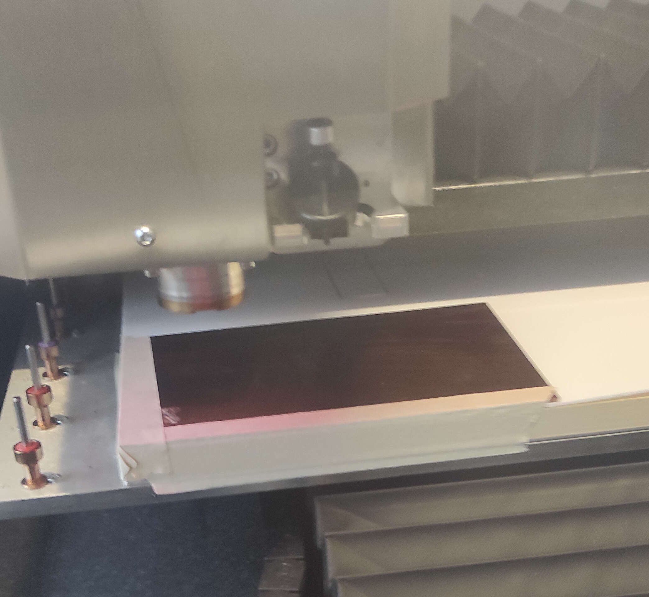
eyeball the position so that the messing colored ring will touch the copper but not the masking tape. when ready click on Mouse cursor in the X/Y - positioning Area again.
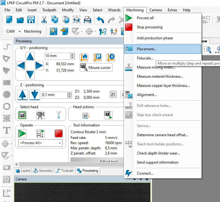
Now we have to place our Board in the cam programm. For that click on Machining->Placement.
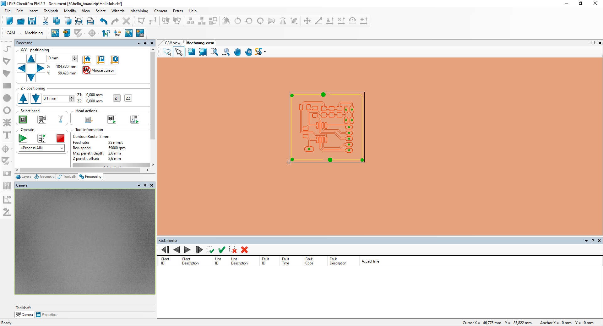
Click in on the position of the Toolhead inside of the programm to set the current position as "zero"
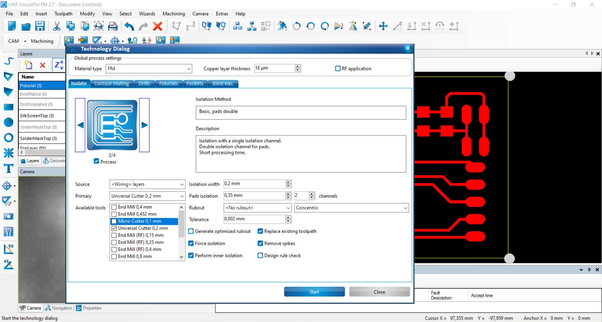
Next Step is to click the red marked menu. This is the Technology Dialog. Her we set the Isolate to "Basic, double pads" by clicking onto the arrows beside the picture. I also recommend to deselect the "Micro Cutter 0.1mm" to save Machiningtime
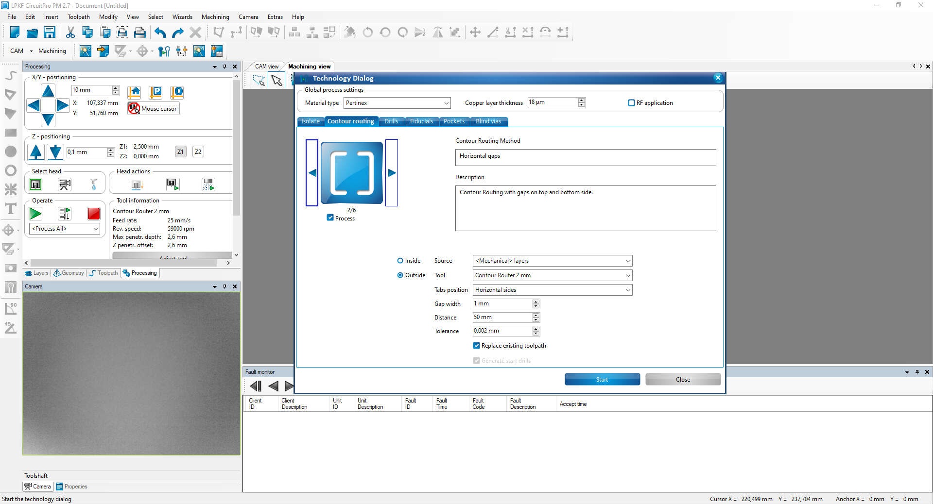
The same procedure for Contour Routing. But here select what you prefer. I prefer Horizontal Gaps in this case. Vertical would be a good option too. If you set the fiducials in the cornors you only can use Horizontal and vertikal gaps. Last thing here is to Click start, to start the toolpath generation.
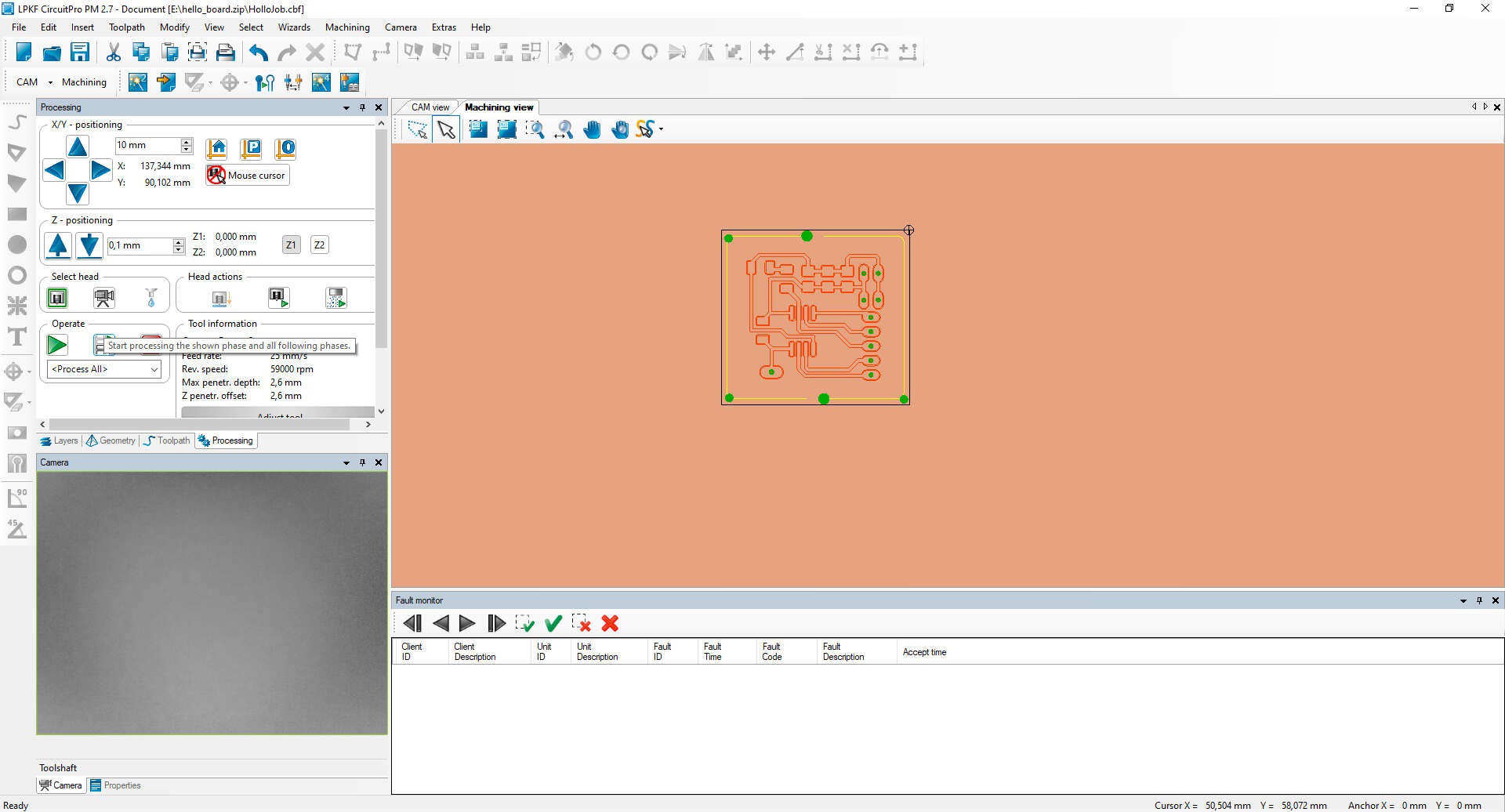
As an Optional step you can check if your Material is big enough by Clicking on the mouse cursour again and click on the upper right corner to move the toolhead to the edge. Than you can eyball the clearance. Dont forget to turnoff the mouse cursour.
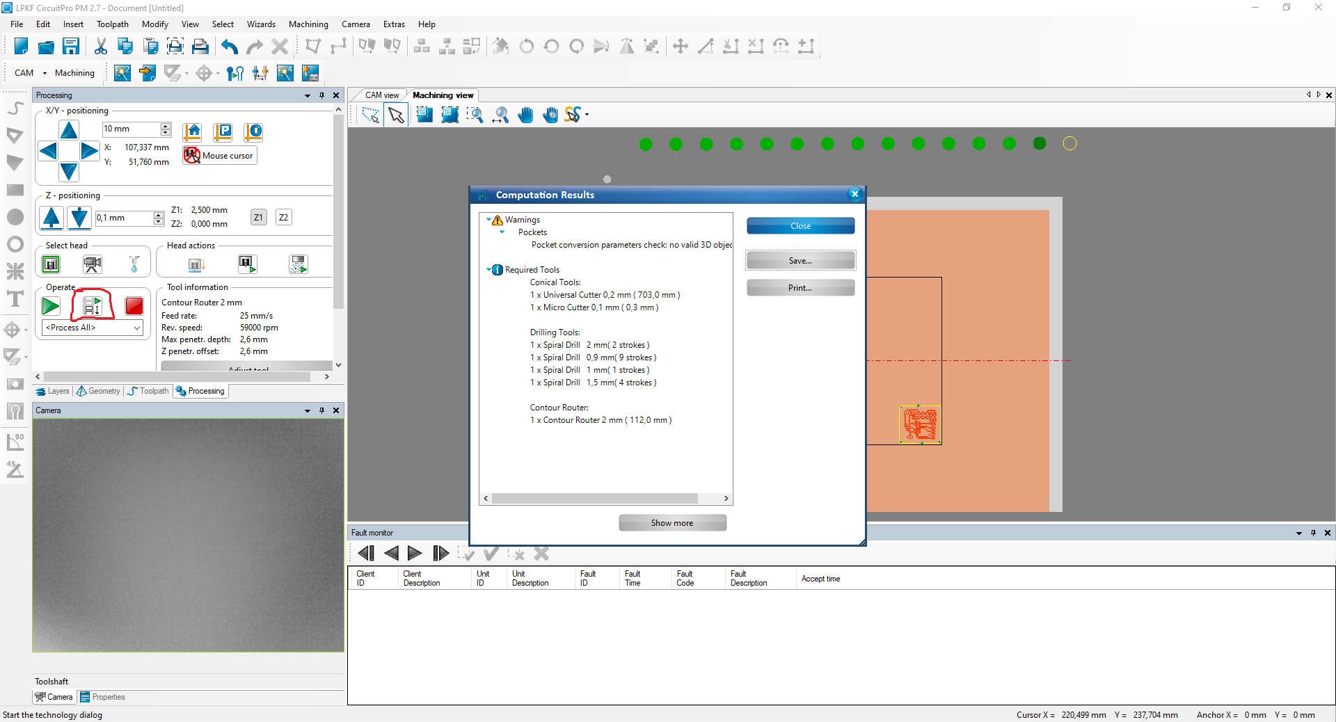
To beginn the millingprocess we need to click the highlighted button. but before we do that we check if "process all" is selected in the dropdown menu beneath. If Clicked we select save and save the Projekt and after that we click on Close
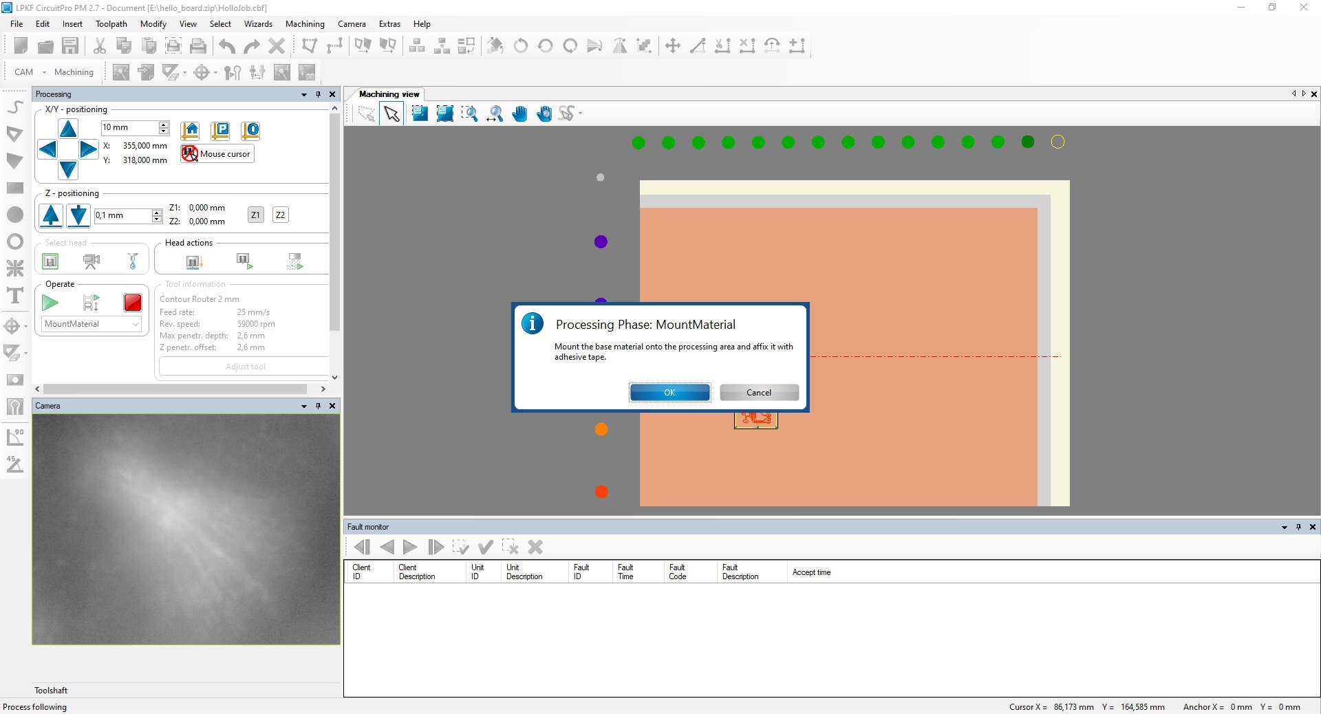
Here we hit close because we already mounted our material to check clearence.
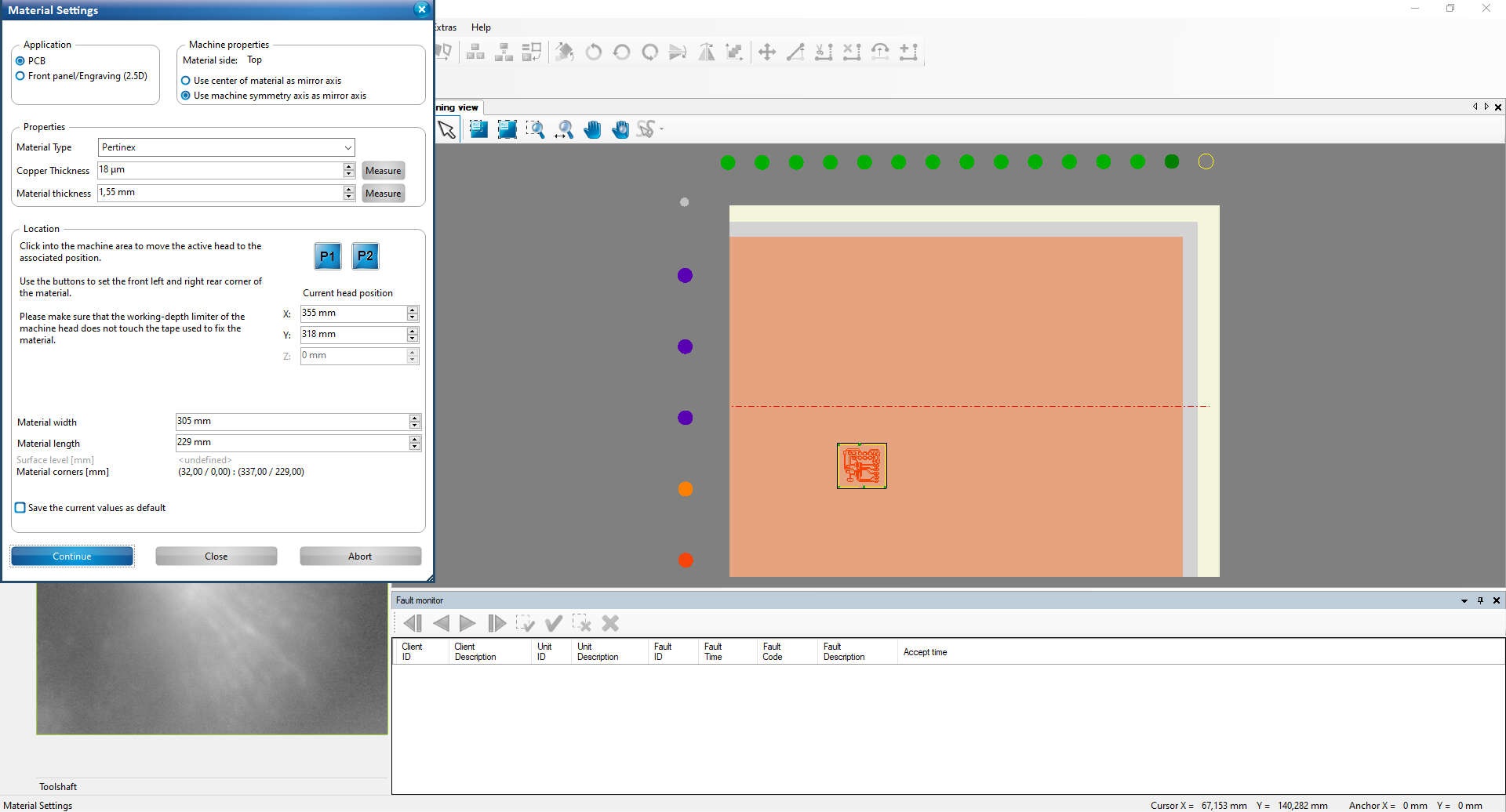
Here change the properties coresponding to your bougth material and hit continue
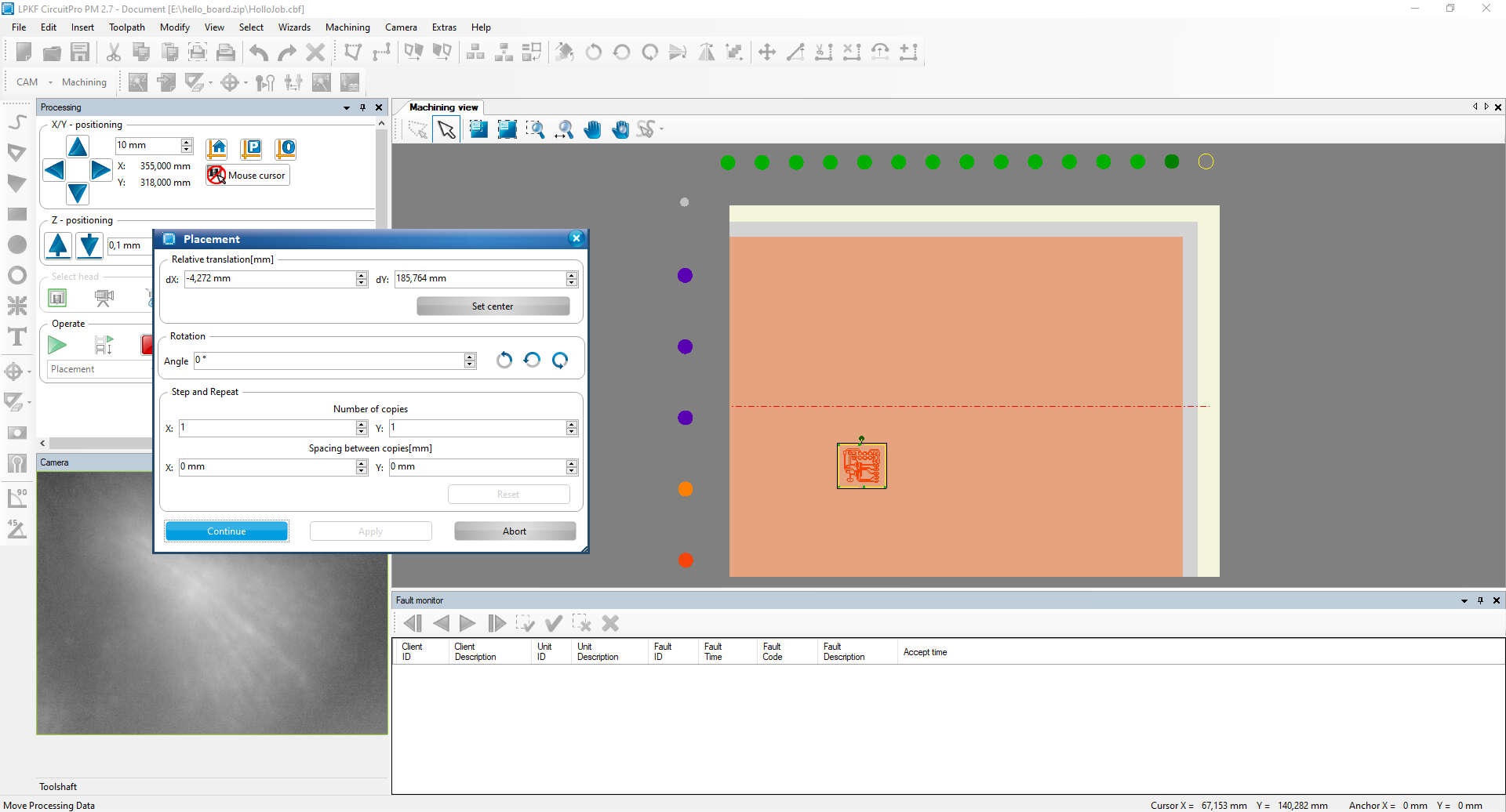
We can skip the placement because we already placed our board.
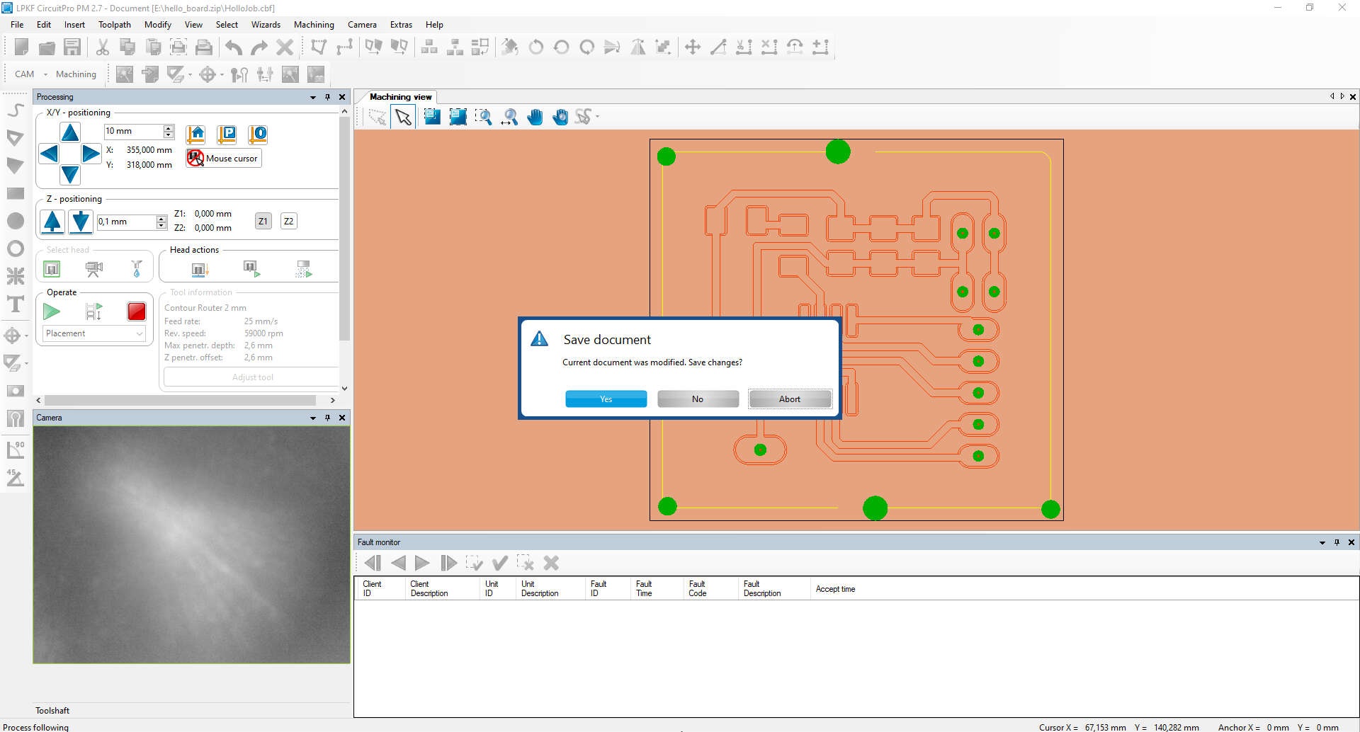
Here I recommend to save again because "DON'T FORGET TO SAVE" and from here the machine makes nearly everything alone. the next step the machine needs your active hand is in the calibration process of the milling tool
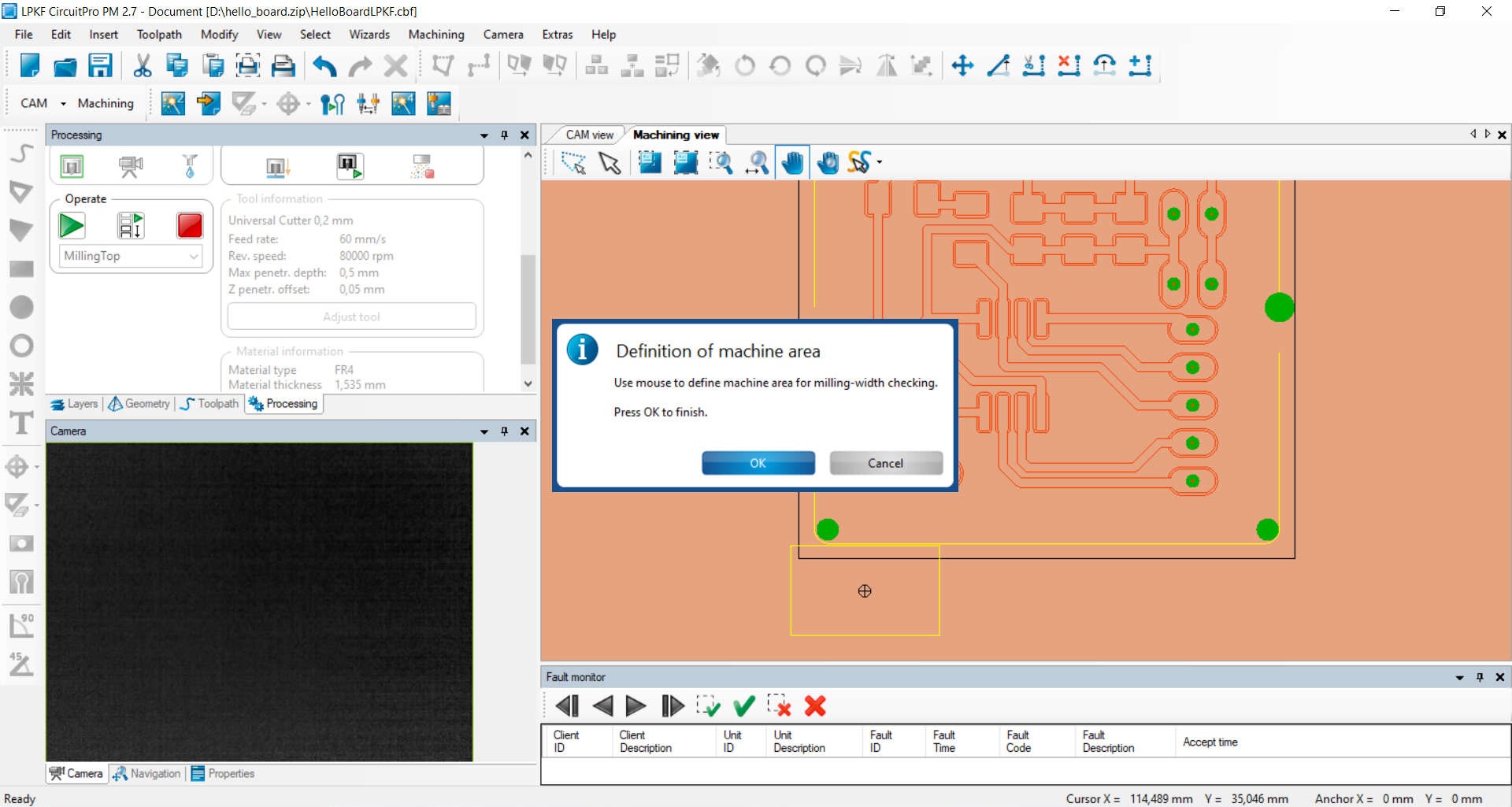
If you followed the Wizard it will ask for a test area to test and calibrate the cutting depth. before you click on OK, click under the the board in the CAM view to define the testarea.
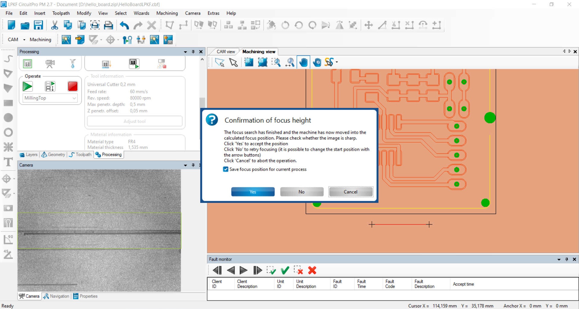
After the machine mills a line with the tool, It will focus the camera on the milled line and you need to aprove, if its focused correctly.
After the focus process it measures the milled width and gives you reccomendations for corrections.
From now on the mill will do everything on its own. And after the Machine is finished, you have to remove the material and cut out the board on the leftover gaps.
Soldering the the Board
for the HelloBoard I needed the following Components:
- 1x ATTiny45 SOIC8 SMD
- 1x LED 1206 package SMD
- 1x 10uf ceramic cap 1206 package SMD
- 1x 1uf ceramic cap 1206 package SMD
- 1x 0.1uf(100nf) ceramic cap 1206 package SMD
- 1x 10k Ohm resistor 1206 package SMD
- 1x 499 Ohm resistor 1206 package SMD
- 1x male Pineader 1 pin
- 2x male Pineader 2 pins
- 1x male Pineader 5 pins
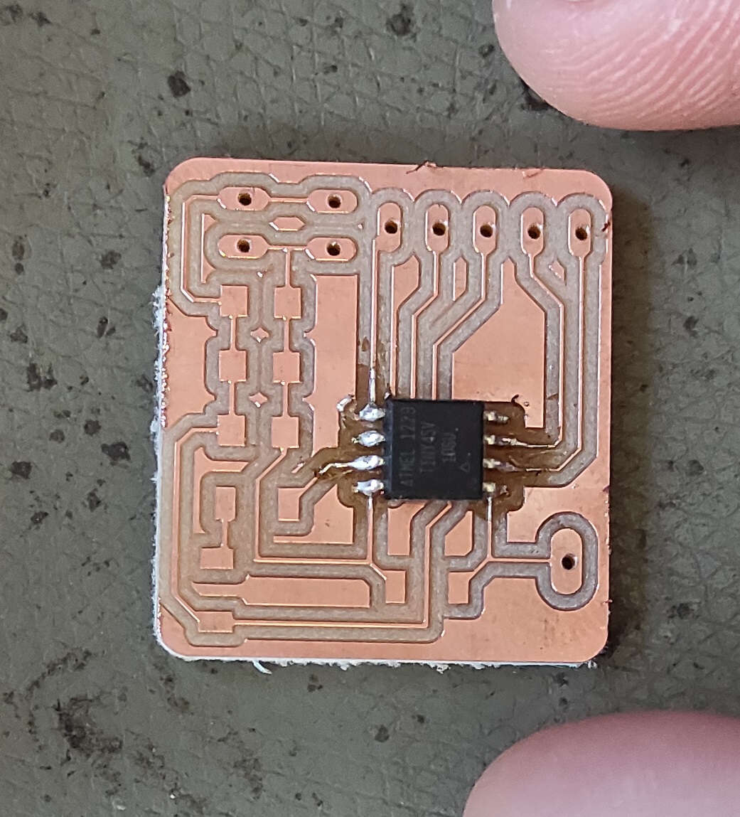
1. I soldered the IC
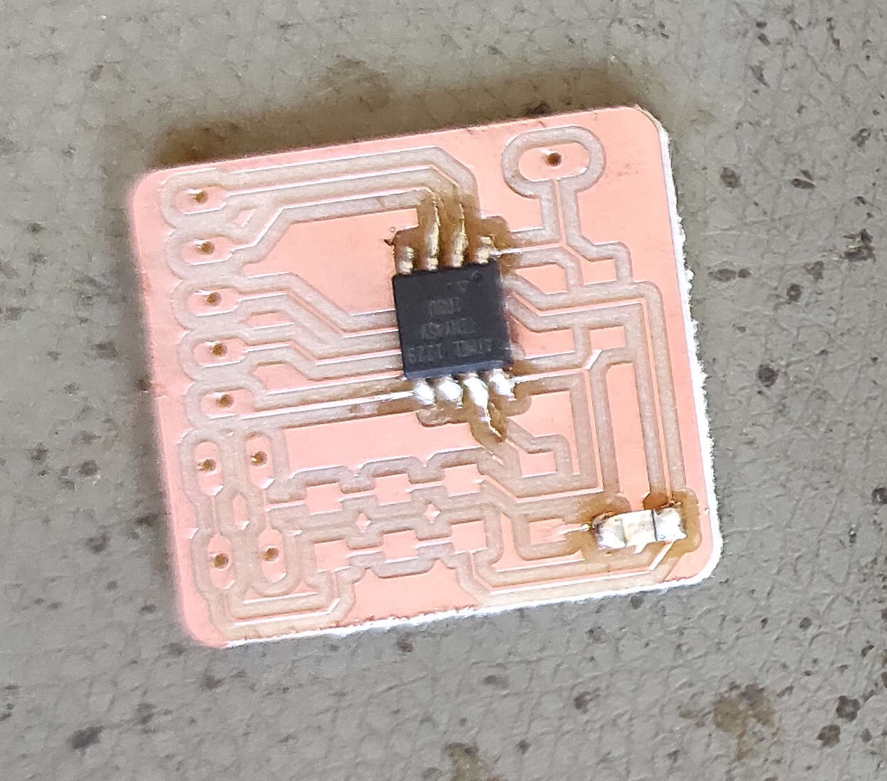
2. I soldered the LED
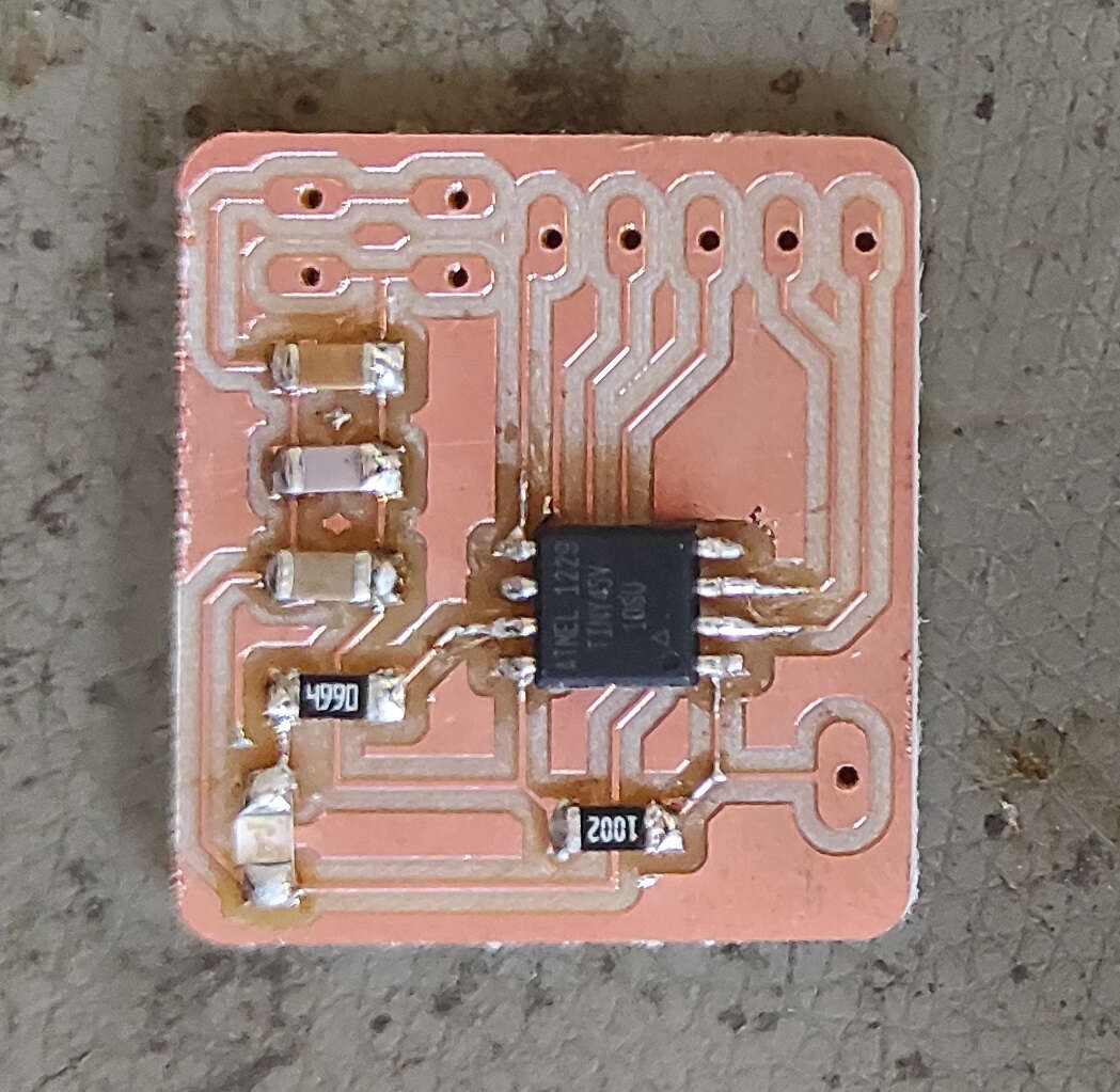
3. The rest is soldered onto the board
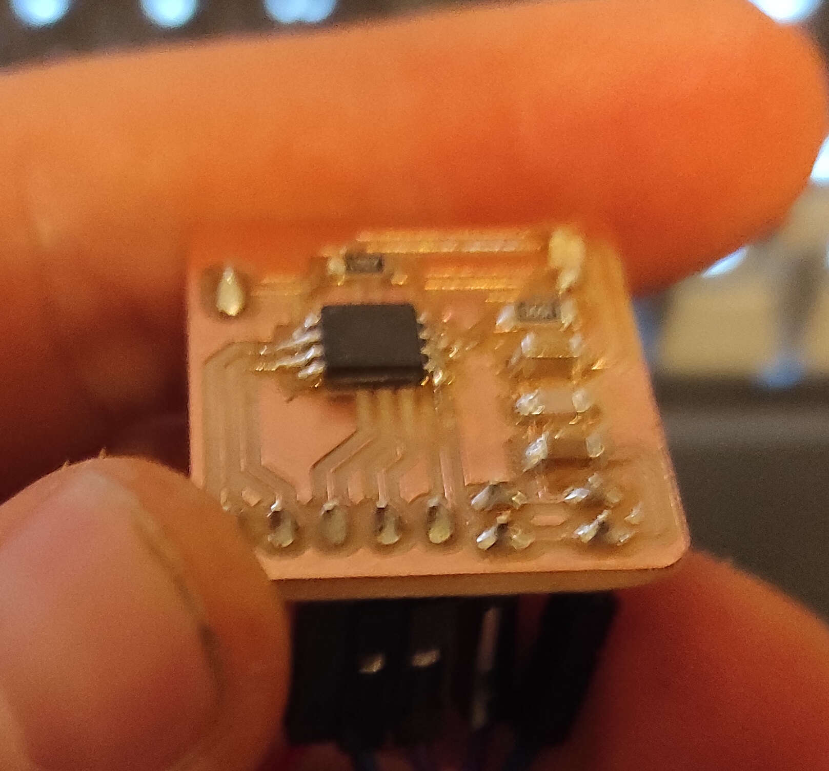
I put the Pin header from the noncopper side and soldered them in place.
Flashing Bootloader and uploading the blink sketch
The first thing I did was to upload the arduinoisp programm to the Arduino Uno.
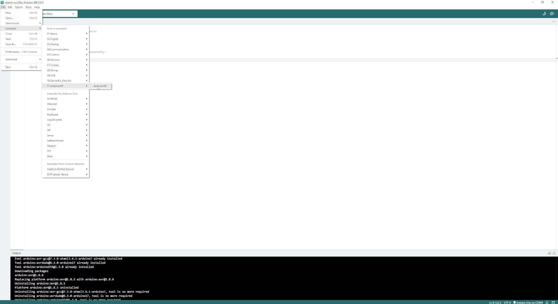
Now go to File -> Examples -> 11.ArduinoISP -> ArduinoISP. If done select your Arduino Uno in the dropdownlist below "help". After selecting your board, click on upload
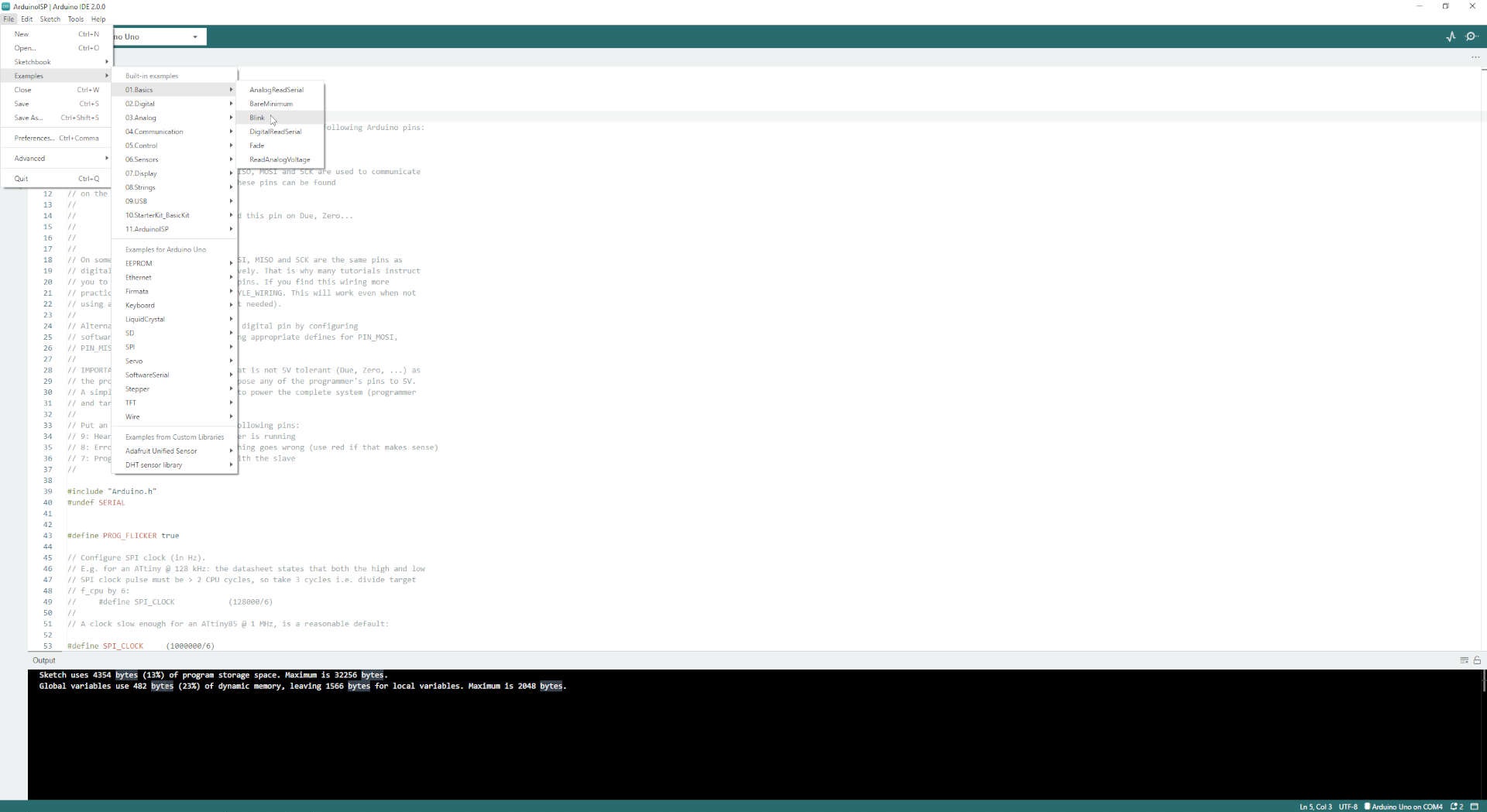
After we uploaded the ISP sketch, we will open the blink sketch (again under examples -> 1.Basic -> Blink)
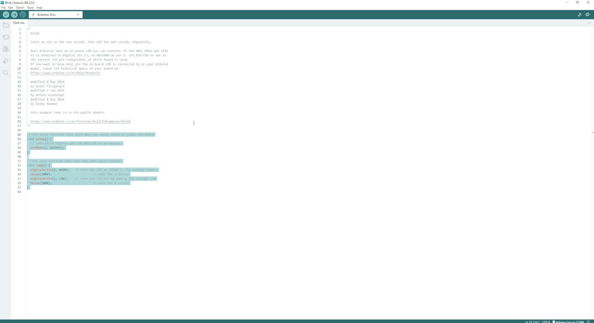
change "LED_BUILTIN" to "2" in the sketch
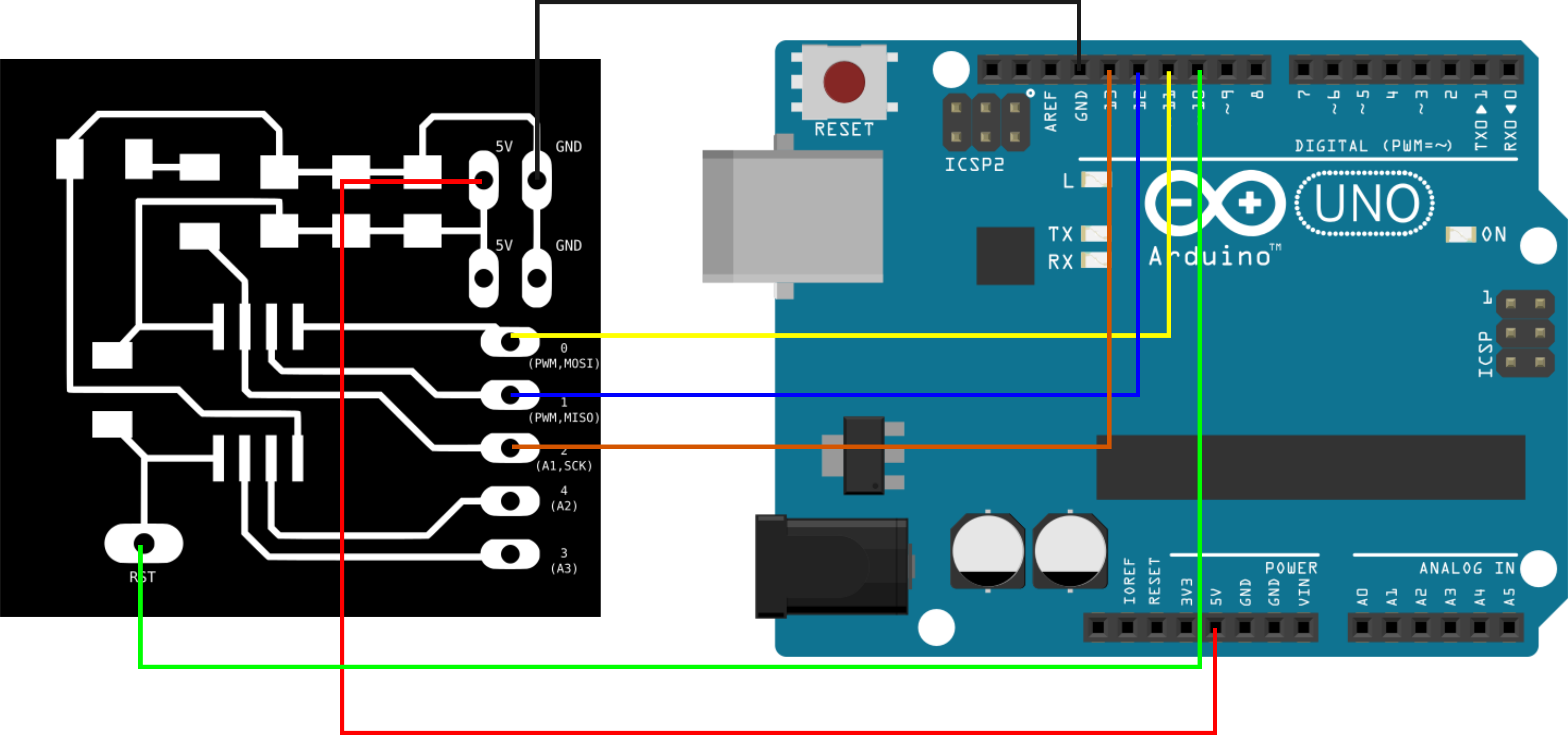
Now unplug the arduino and connect your soldered board to the Arduino Uno like in this Diagramm.

To setup for burning the bootloader, you want to open File > Preferences.
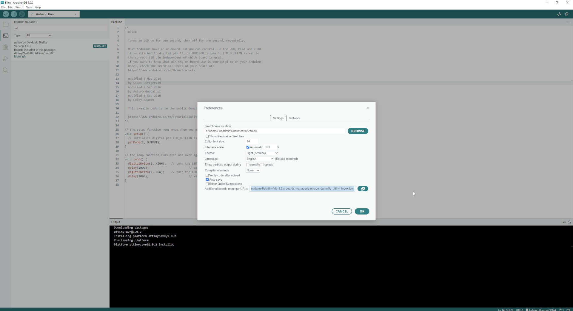
Then, at the bottom of the pop up menu where you see "Additional Boards Manager URLs" you want to copy and paste "https://raw.githubusercontent.com/damellis/attiny/ide-1.6.x-boards-manager/package_damellis_attiny_index.json". Click on OK
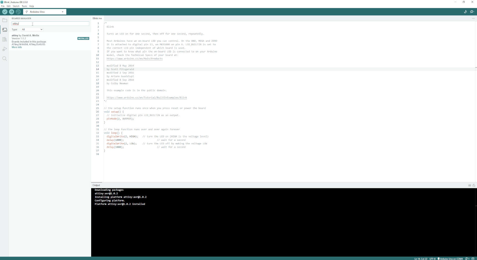
Navigate to Tools > Board > Board Manager. The Boardmanager will open on the left side. here you search for "attiny" and install the in the Picture shown Board Library
at this point we can connect the Uno to our pc again
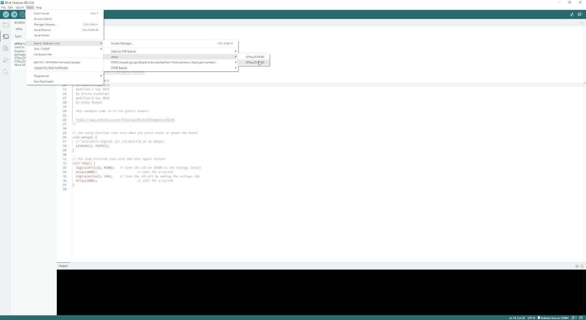
Now we navigate to tools -> Board -> attiny -> attiny 25/45/85 and select it

the clock is set in tools->clock to internal 8mhz

the processor is set to attiny45

Now we can decide: do we want a bootloader on it? In our case it doesnt make any sense because we dont have any connectivity for an ftdi cable for example. But if you want to do it, click on burn bootloader under the tools options.

now we can click on uploading over programmer to programm the blink sketch to out soldered board.
FinalBoard V2
To get ahead, i needed to Mill my PCB i designed in Week 6 this is the first actual Version of my PCB for the Final Project
Milling the Board
To get started i first setted up the job like above but with some Changes. The first change was to select the double sided Template.
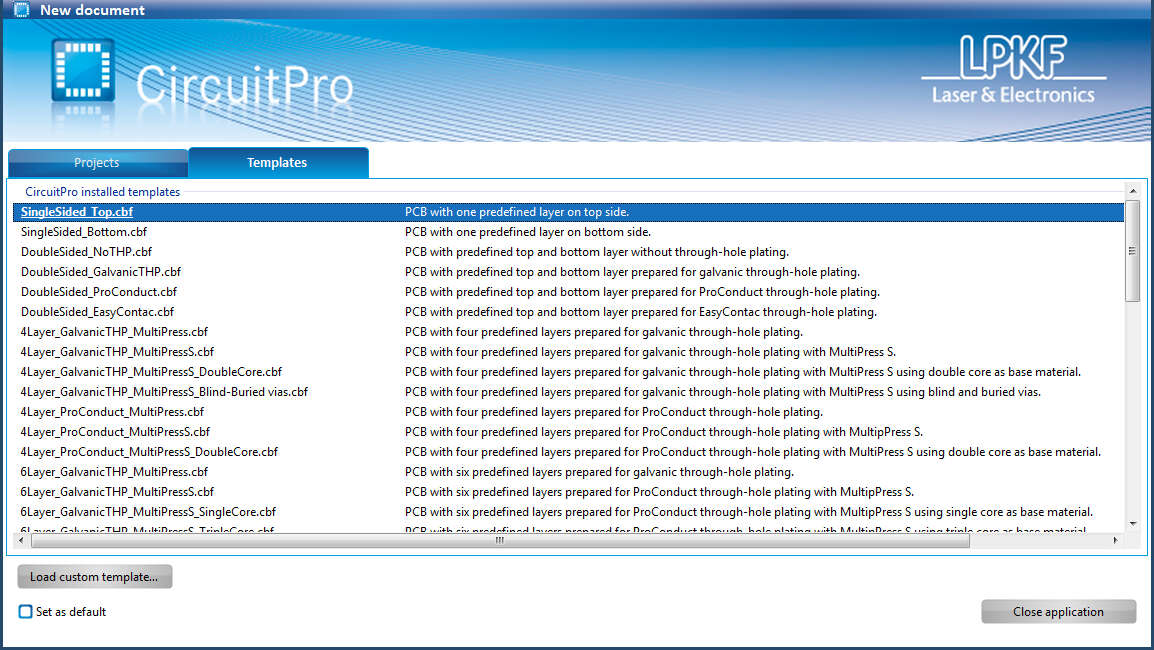
Second was to import my Gerber Files.
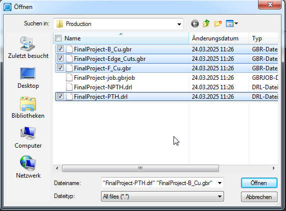
Followed by checking if everything was rigth.
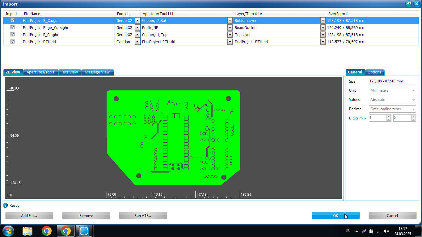
Then changing the Technique to Drilling and the Phase to Dripping Plated for the from the Software created DrillJob.

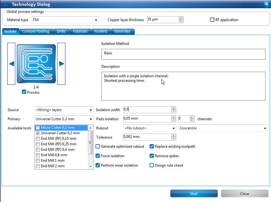
Then going into the Technology Dialog and change under isolate the isolation methode to basic and the isolation width to 0.5mm. Also untick the 0.1mm microcutter, that only the Universal cutter 0.2mm is used.
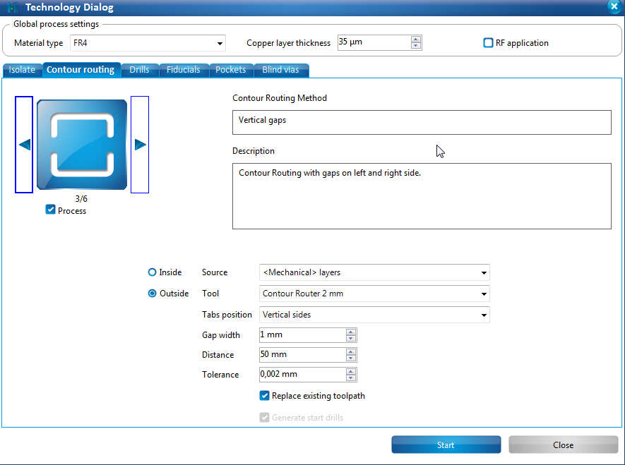
For the Contour i went with Vertical Gaps.
Now i did everything as with the HelloBoard and just followed what the Programm asked me. The only aditions where flipping the Board and reading the fiducials. One Hit from my side. Mark where your board was. I forgot that and Just eyballed the location, what lead to the fact, that i had to Manually align the Camera with the first fiducal.
Problem 1:
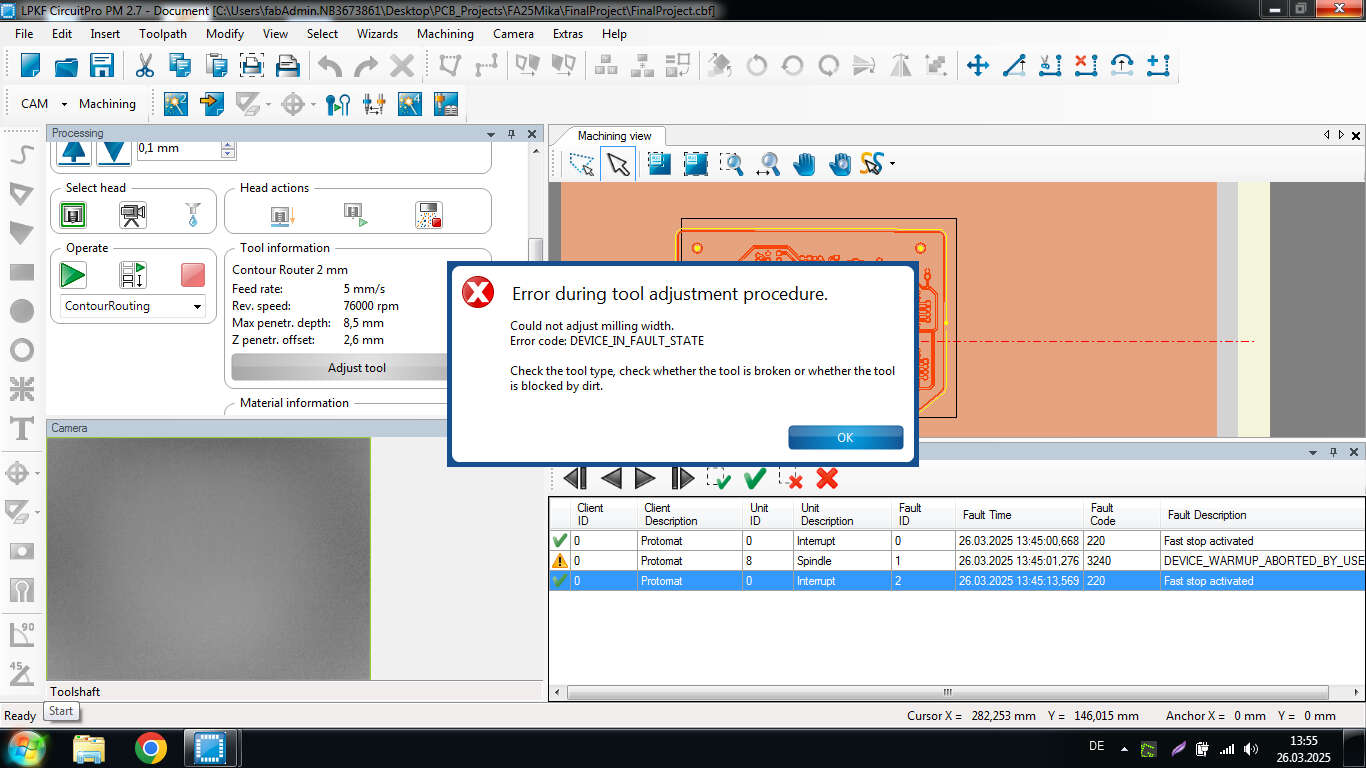
My first Problem was at the End. The machine gave a weird error. It was in the phase of picking up the cutout Bit and calibrating the heigth, as i got an error that the machine could not adjust the mill width. We checked if the tool was broken or dirty, neither was the case.
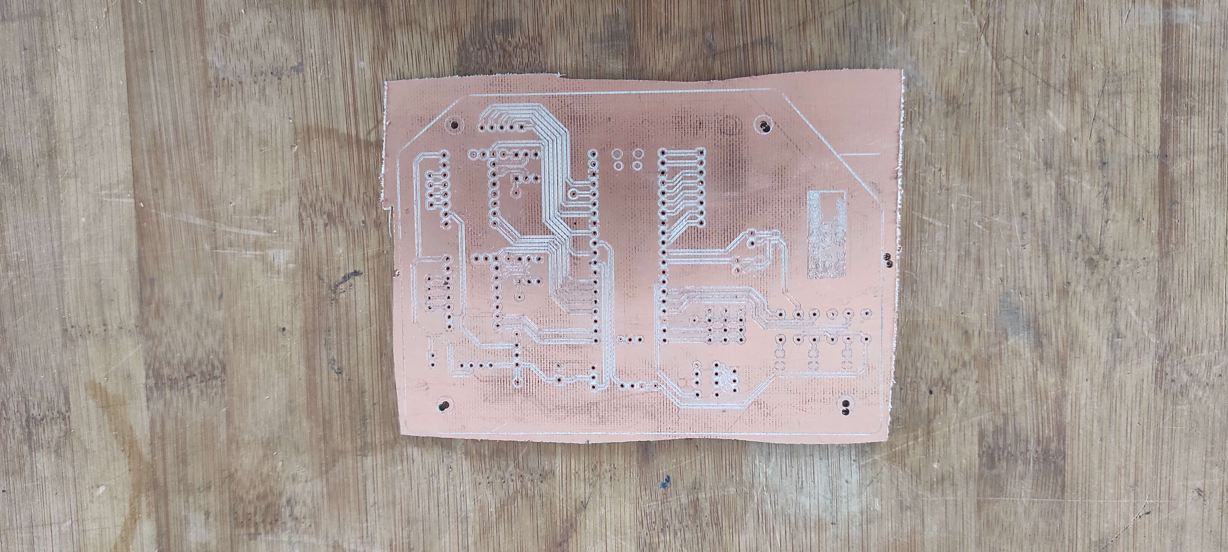
I then pickedup the board, equiped me with a hacksaw, a Mask, safety-glasses and some glass and rough-cut the PCB.
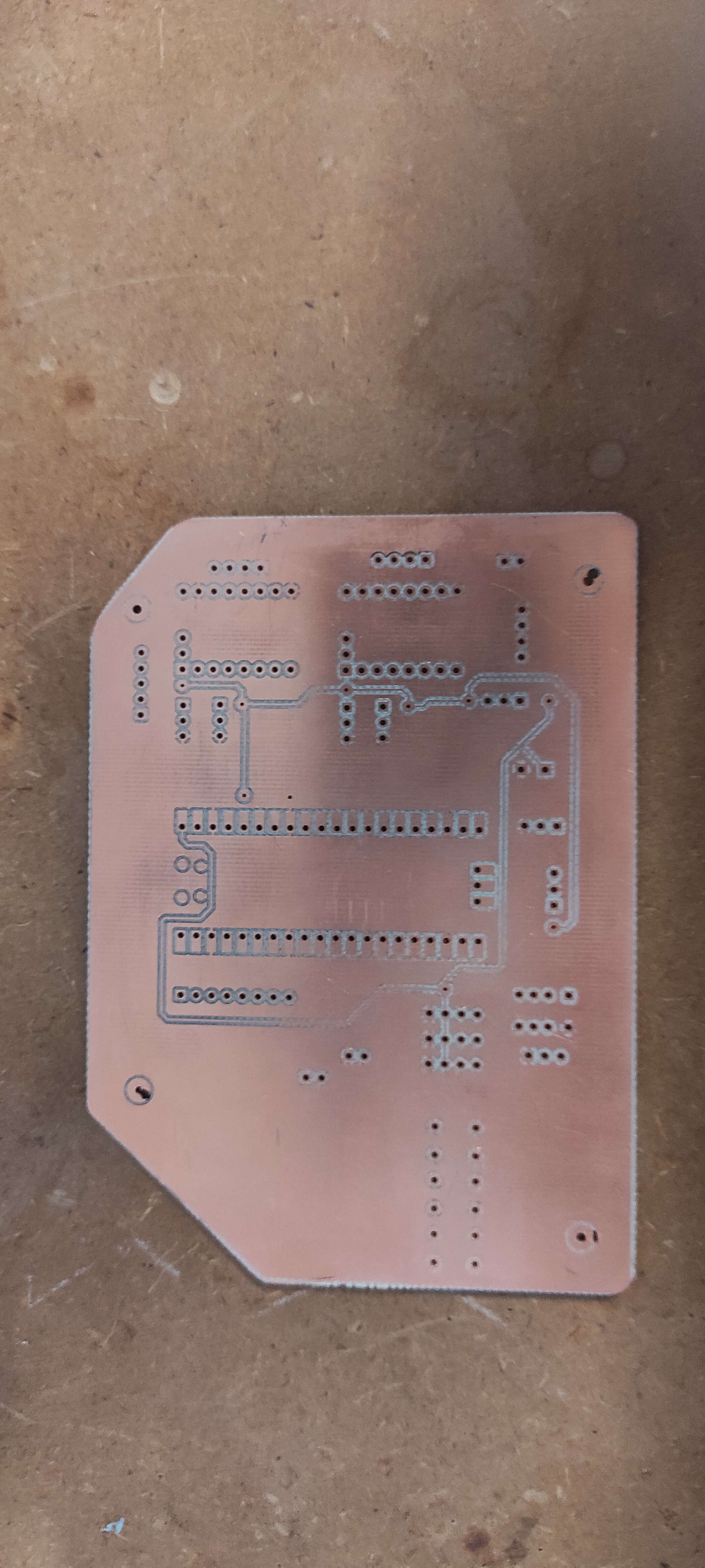
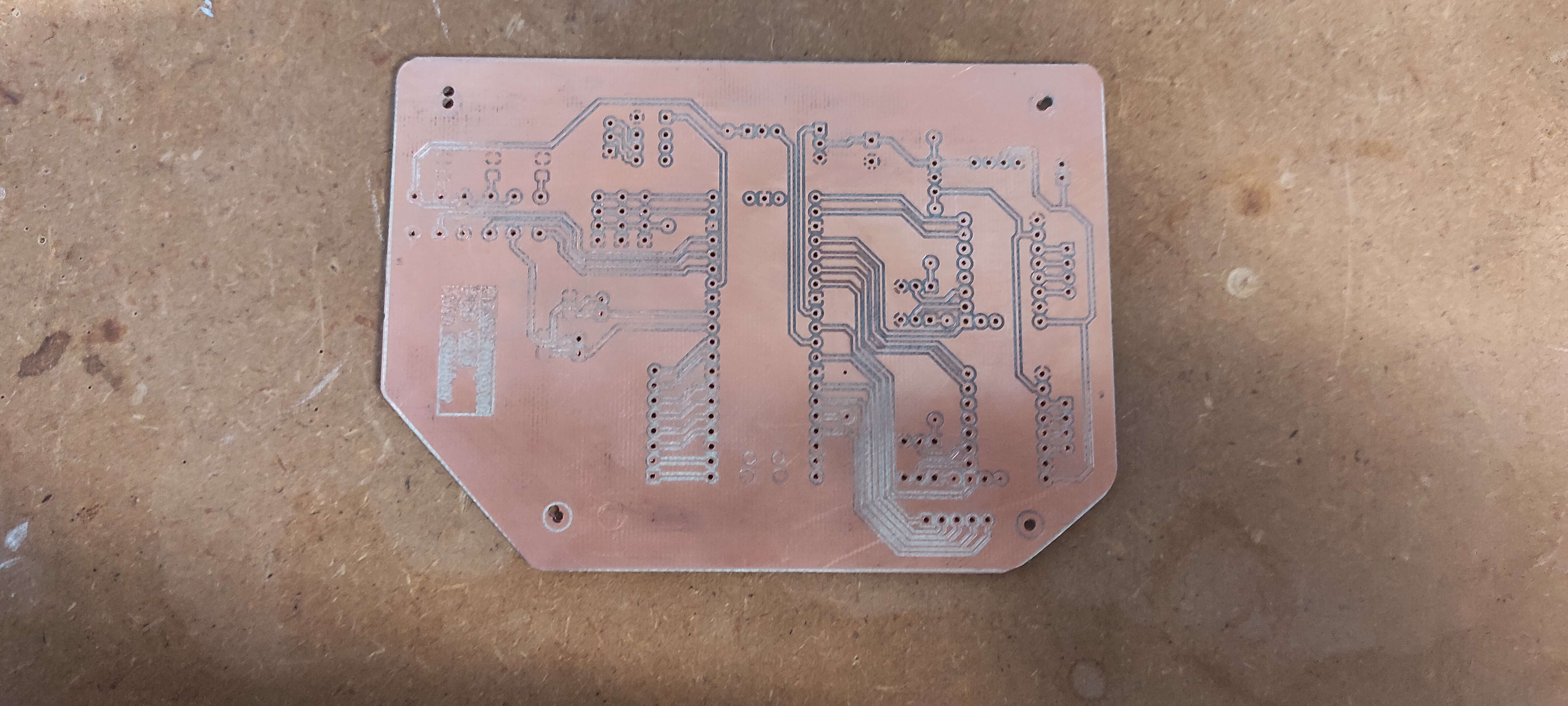
I finished the Job by sanding all the edges to the milled outline.
Vias and Soldering
As you remember i used some Vias in my board. I also had a small problem here. On the packaging of the used rivets stand the size 0.6mm. I assumed that was the puter Diameter, but it was the inner Diameter(and i didn't measured bevore milling). The Outer Diameter was 0.8mm. So I quickly put a 0.8mm drill into our Dremel in the Drillpress and Drilled all Vias a bit larger
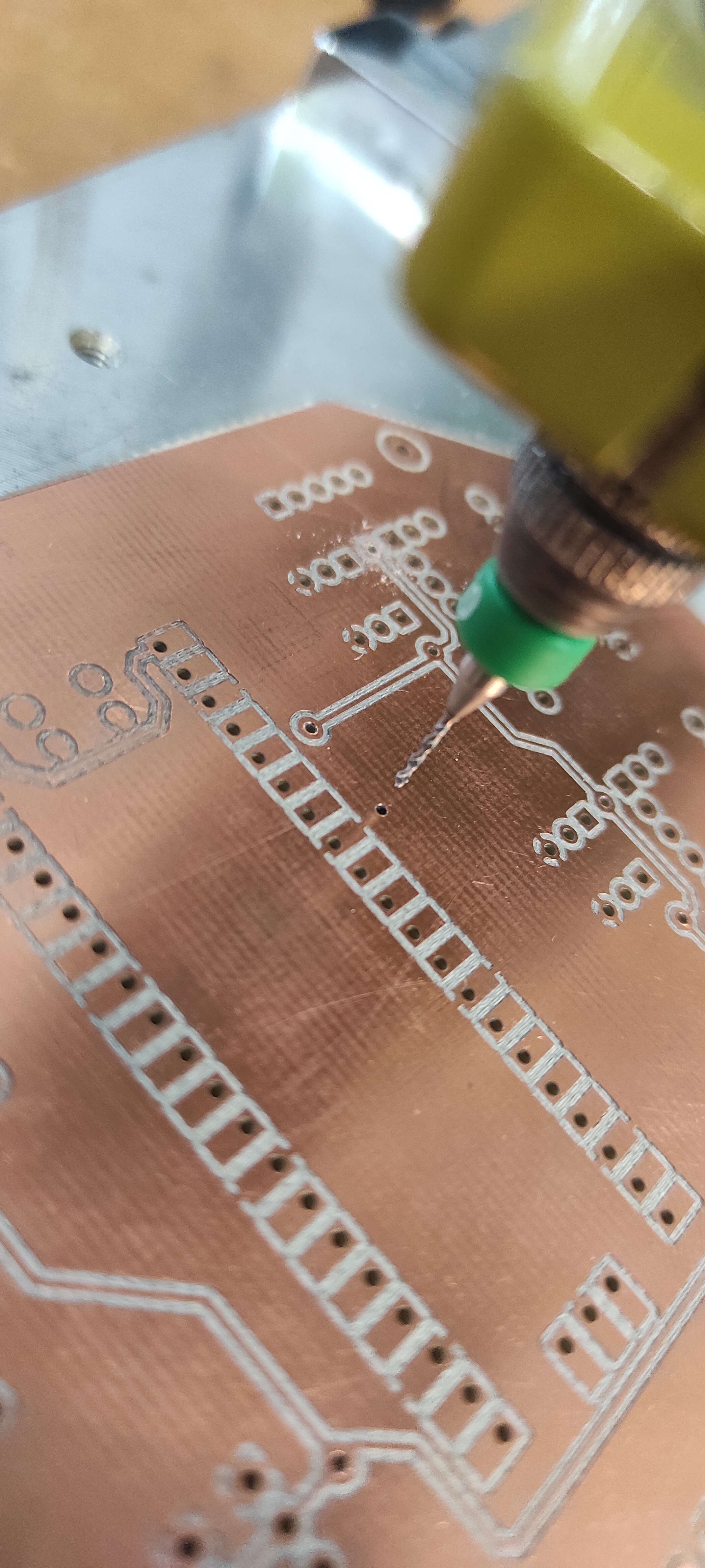
Said and done, i could add the rivet into each Via and press them with the press.
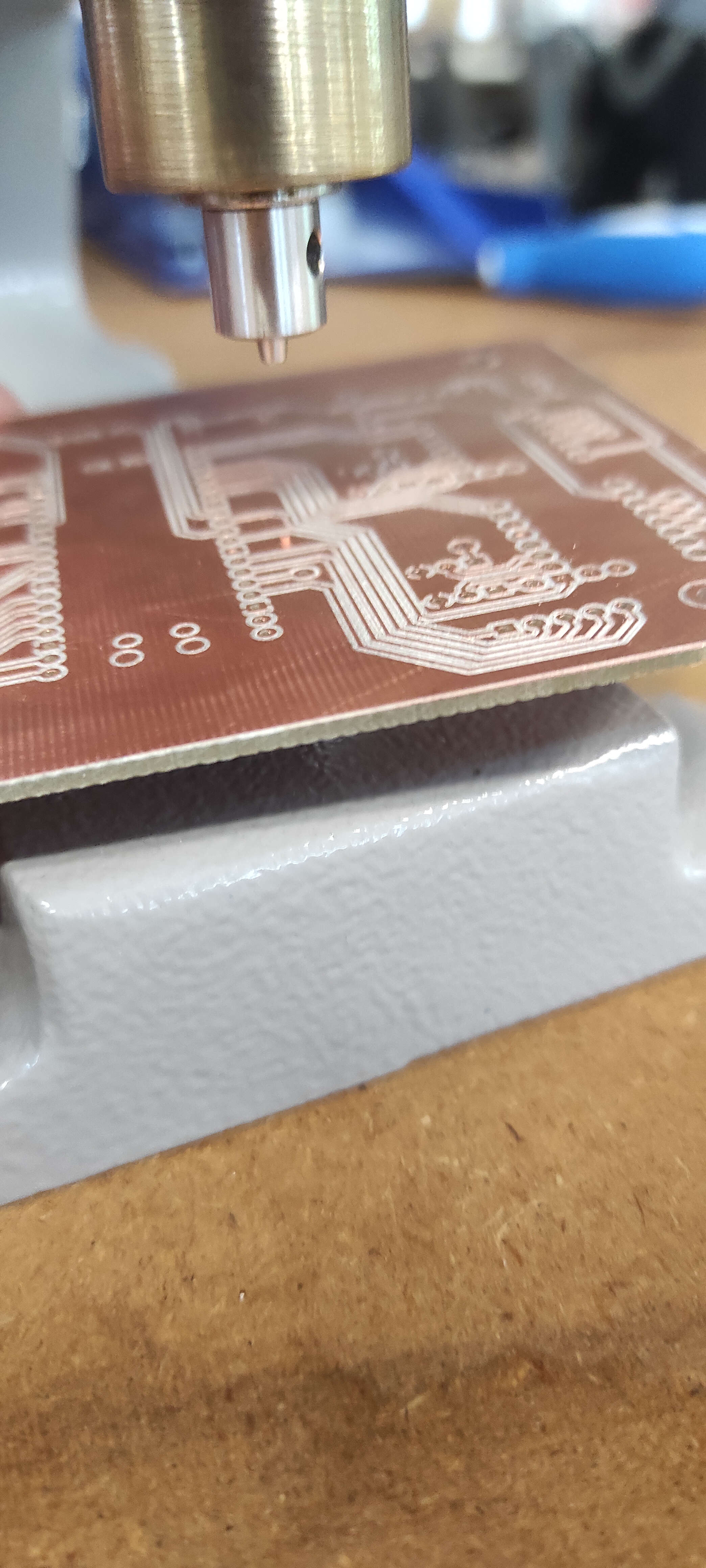
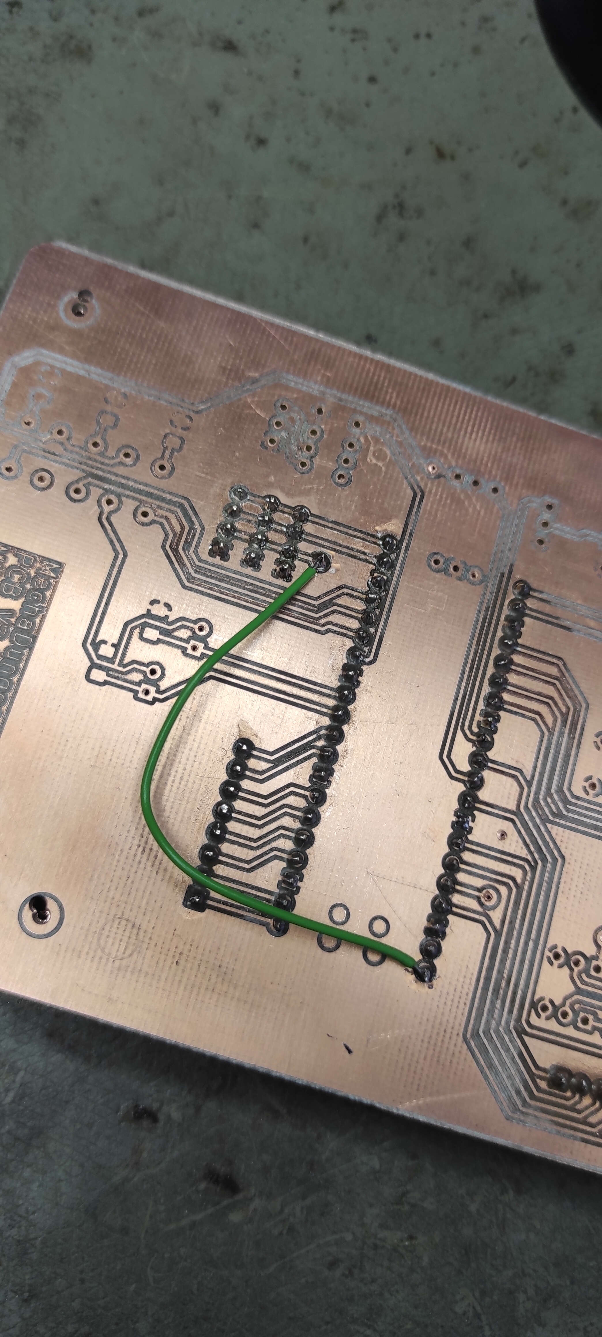
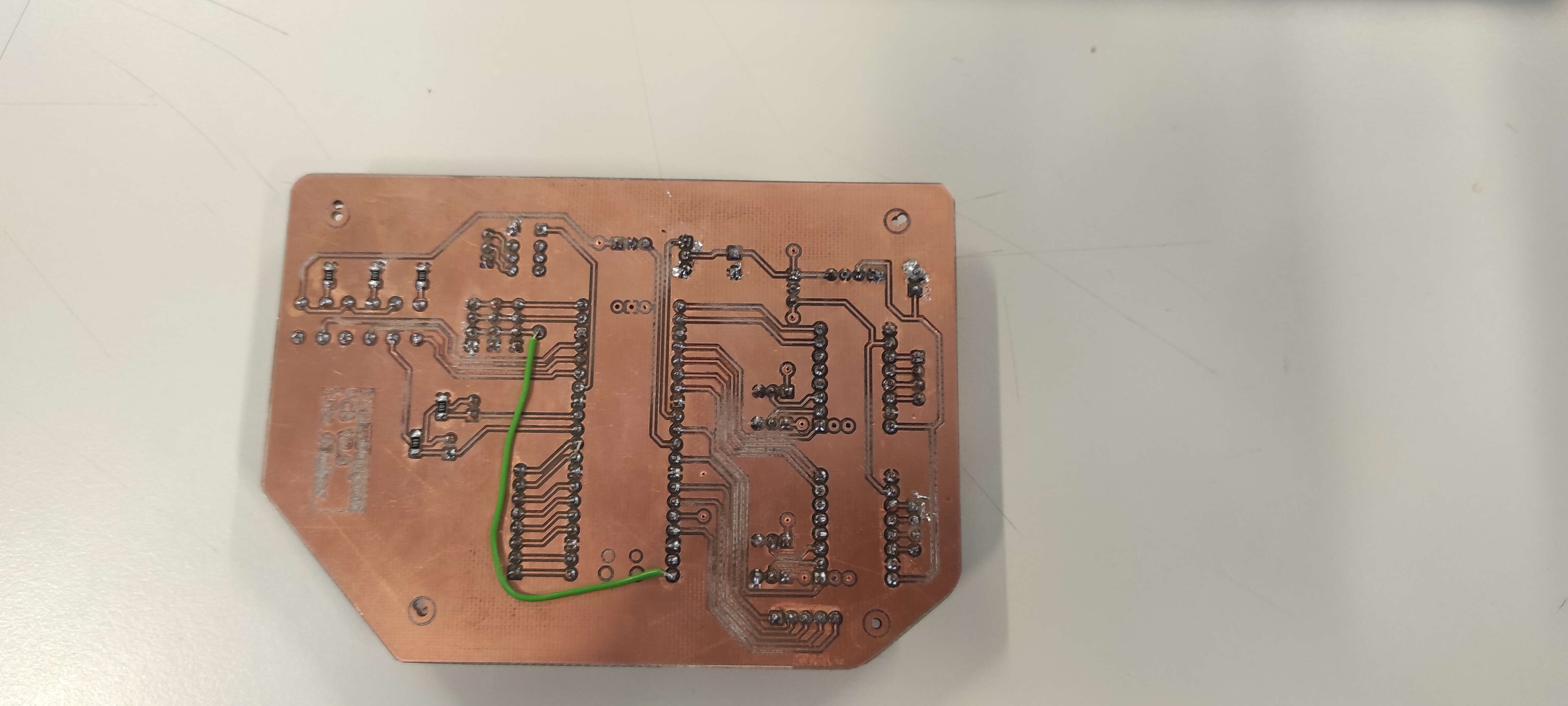
Now was time for another fail on my side. You can deside: either i forgot that the Holes are not Plated or i forgot to add a 5V Via to connect the bottom of the VBus to the top. My fix was easy. I soldered a wire on the Top side of my board, from the VBus of the Pico to the 5V Via/Rivet near the I2C Pins.
Last Step was to solder the female pinheaders for my Pi Pico aswell as the male pinheaders for the Leftover Analog and Digital pins and also the pins for the spare power and I2C Breakout
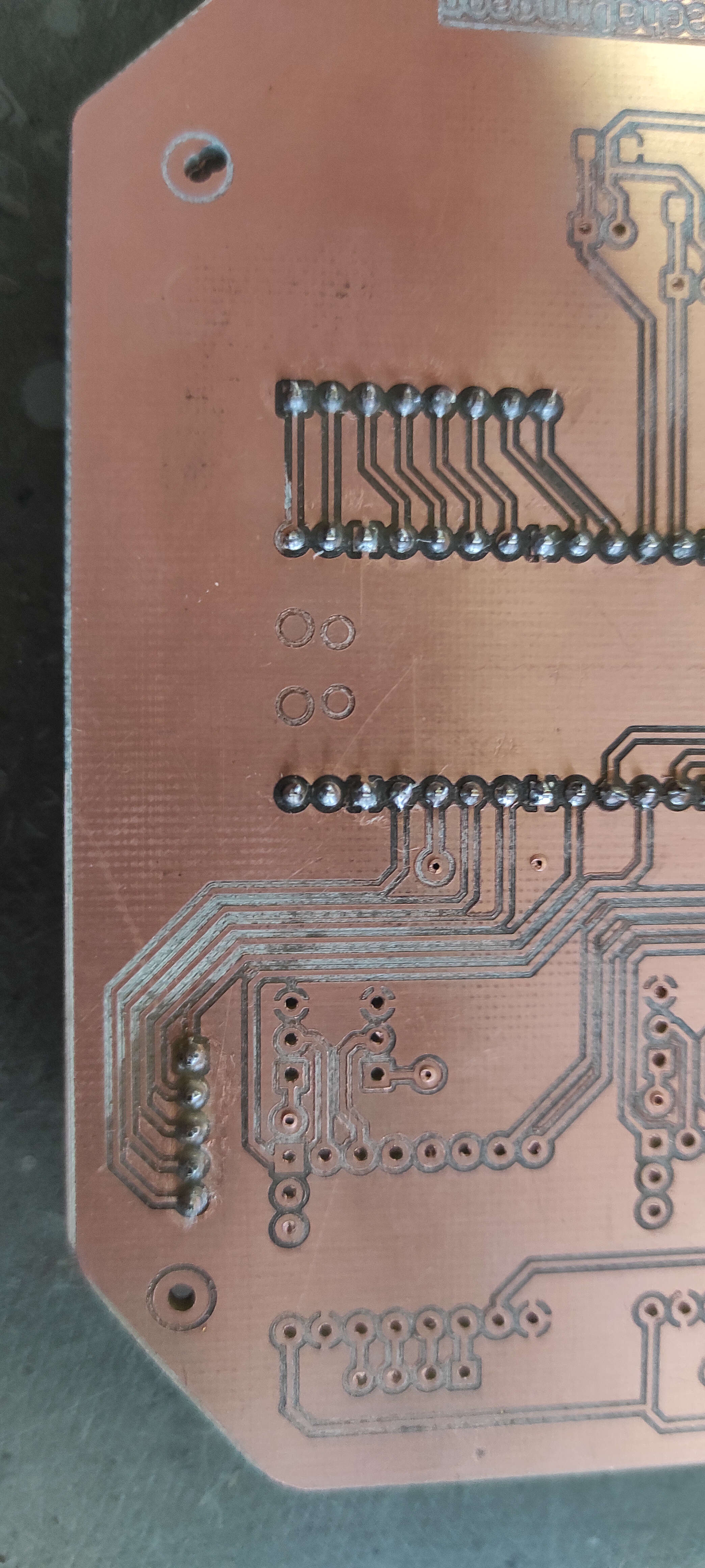
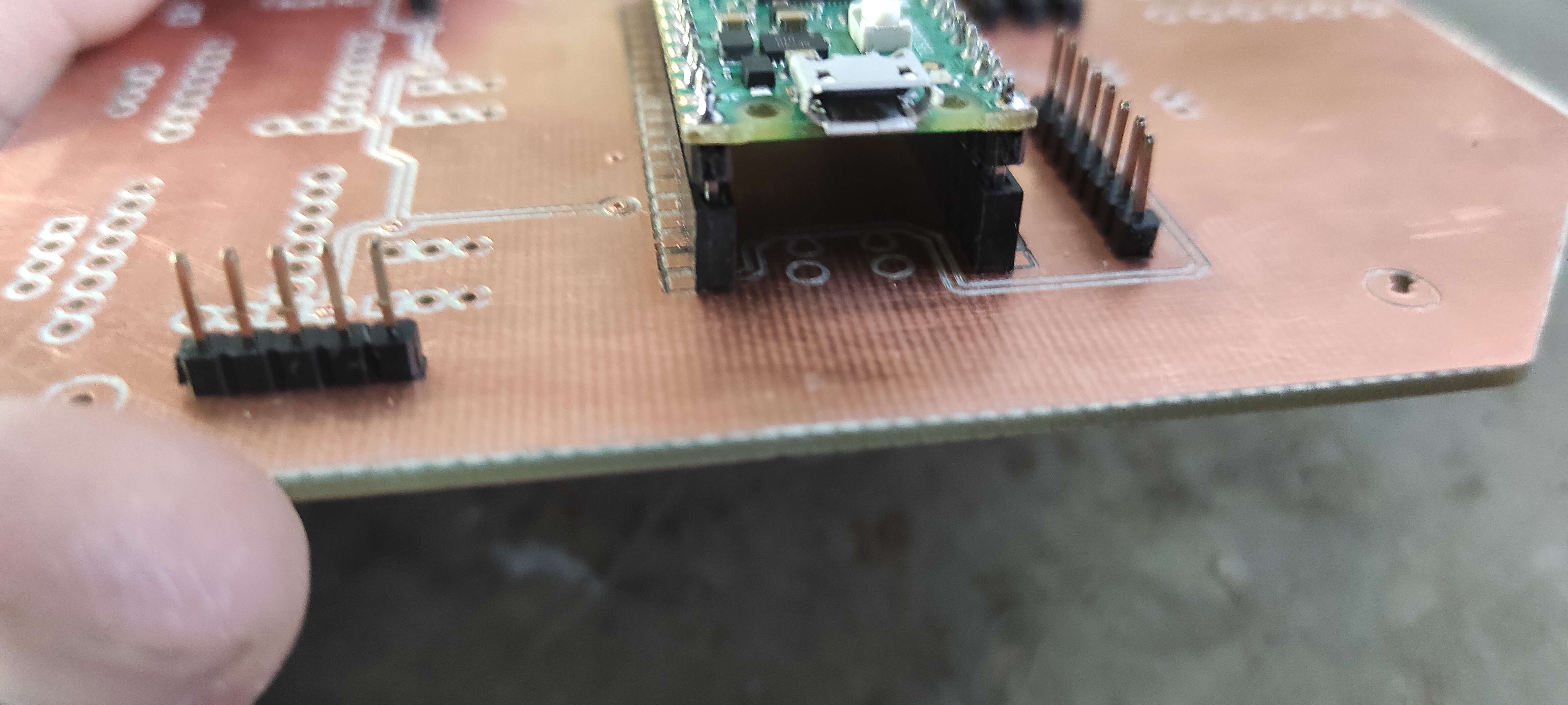
fully assembled
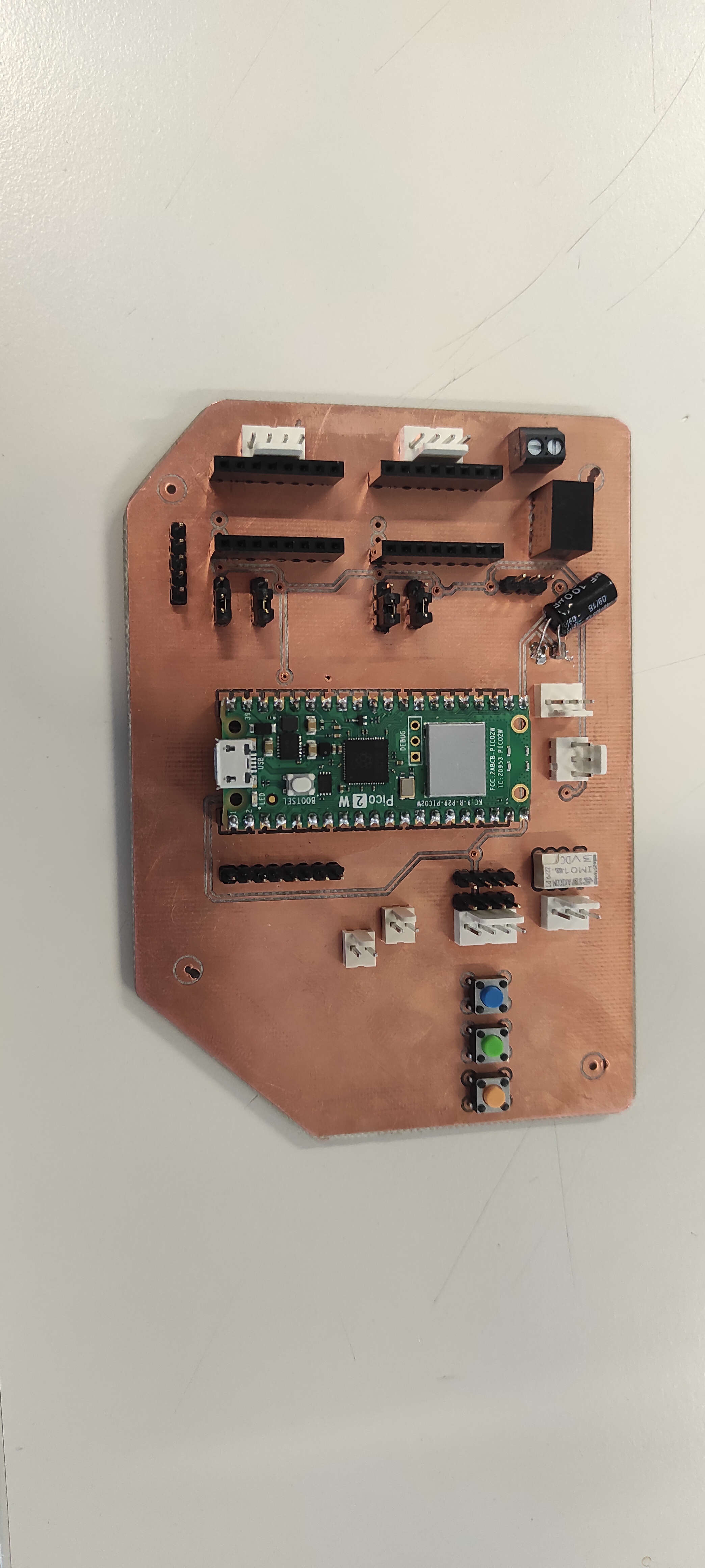
Here you can see my board fully soldered./p>
Does it Work?
Because of the Conference i was at, i did Week 8-10 in one week and thats why you see in Week 9 and Week 10 that its working!