06 Assignment Electronics Design
Part of this weeks assignment was to test our electrical devices, the multimeter and the oscilloscope. This was done as a
group assignment. This a simple process, there are countless videos on this subject online.
The second part of this was to learn how to use the software Kicad, which is
a free software and comes with a large library of Electrical parts and footprints. The software allows you make your own schematics and
Printed circuit board als known as PCB. These boards can be made in different ways some need to be printed with special toner
transfer or UV exposure and chemical etching or can even be routed with a V-grove bit. The professional boards are manufactured
using CNC machines, photolithography, and automated assembly with multi layers printed on top of each other. The goal of this
assignment this week is to use a software that allows for the Design of the board.
Kicad for PCB's development
In the past you you would of had a board with lots of holes and you would add the wiring to make the circuitry. Today you use a breadboard for prototyping. I would also recommend that this as well with either a simulator or buying a set to build circuits at home or in the lab. I talked about this in embedded programming. Once you have downloaded and installed Kicad and installed the Fab-Academy library which we where talked through by our instructor who also gave us a crash curse in how to use Kicad. I found that it also helped to go through a couple tutorials. I wont provide a link as there are different tutorials that may suite your needs or personal preferences. I can however for the total beginner recommend this video to get you started.
I am by no means any good at Electrical Design, nur do I have any real know how about Electronics. This why I recommend building the circuit
you
want first and making sure what parts you need to use and running test. The second part you should do as I did look at the data sheets to make sure
that you are picking the right part with the right voltage. Even comparing the data sheets with alternative parts. As I will also have a small DC motor
that needs to propel smoke through a small pipe in my wind tunnel to show the flow of the air around the object. Knowing that running a DC motor off a
micro-controller will kill the boards electronics I needed to look at making a H-bridge. there are many different ways of building such a circuit
, and
never having made one I read a lot on the theory of H-Bridges.
Why is it called an H-bridge? The fast and easy answer is that the ciructe looks like an "H". Basically this circuit is made to control the direction
of a DC motor. It is made up of either 4 transistors or MOSFETSs and for some protection of the ciructe resister were added.
Parts list:
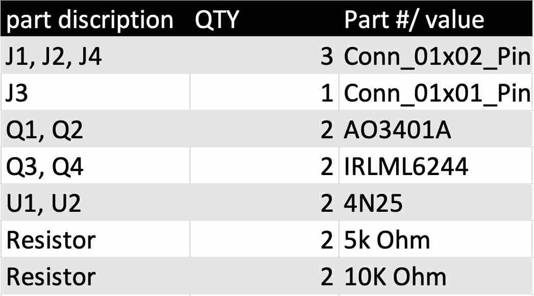
Once the details of the circuit were clear everything including a sketch of the circuit was made on paper to make sure nothing would be left out and all
the connection had a place to go we can start by lunching Kicad. Go to File > New Project, in the menu give the file a folder and name the project.
Now go ahead and select Schematic Editor.
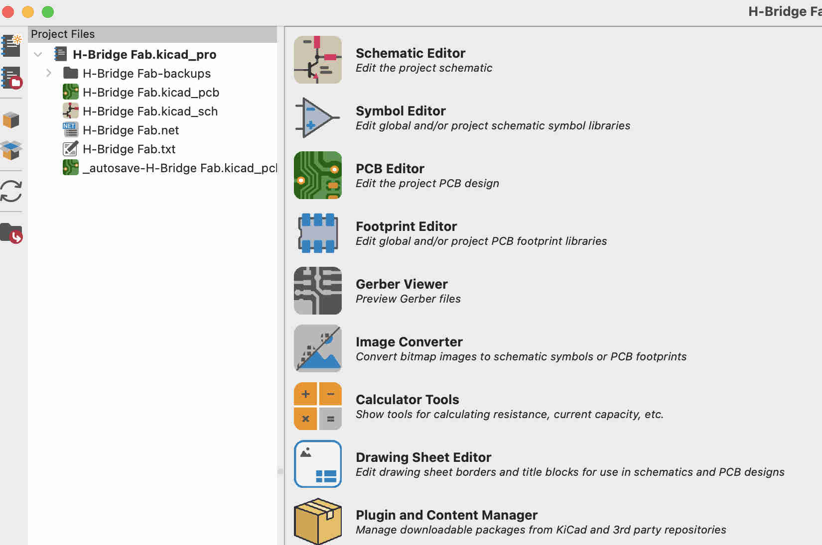
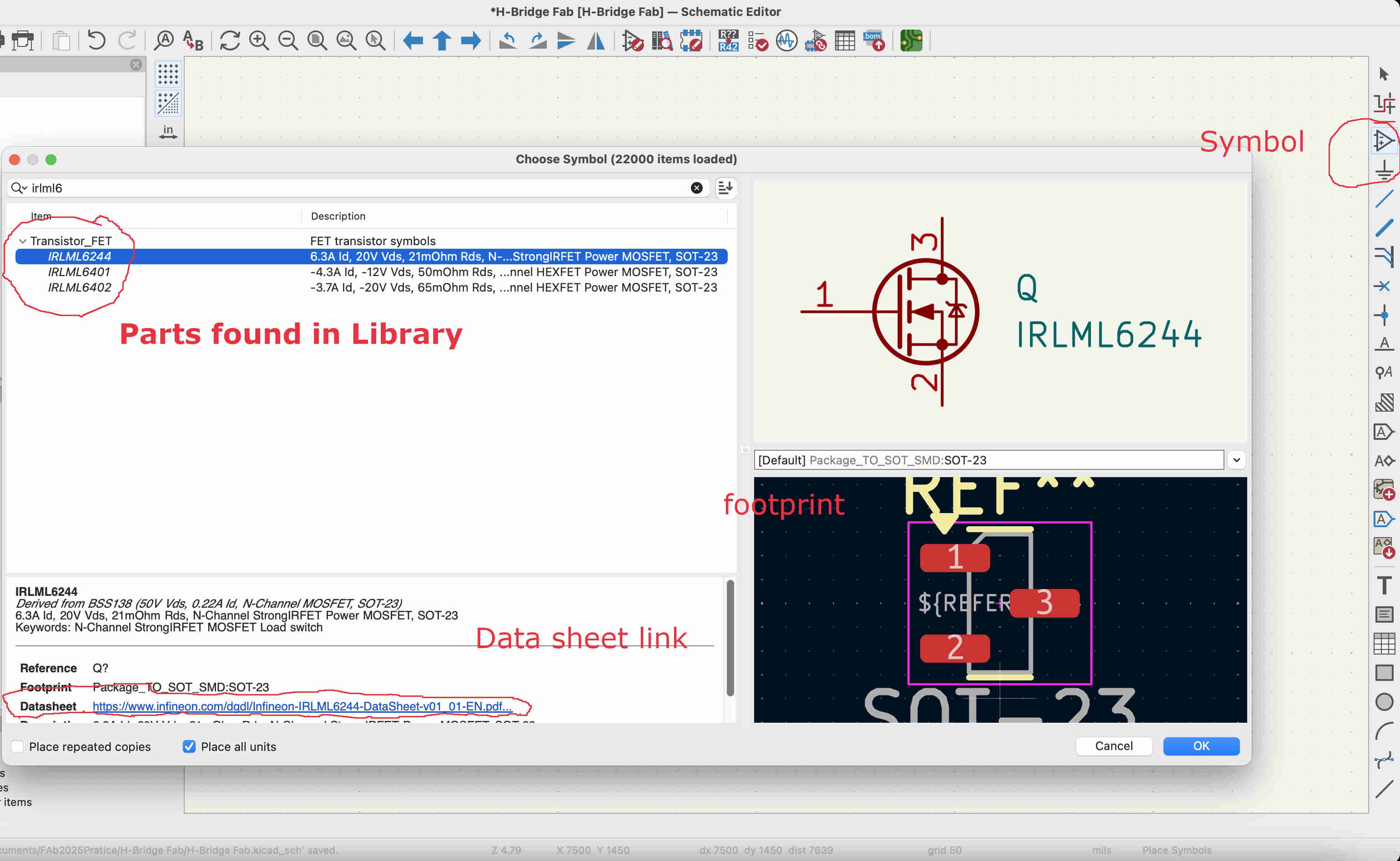
Now that Schematic Editor is open we want to add the parts from the list above. This is done by the use the add symbol button. Here ypu can
find all the parts and some of the footprints that the parts have as well as size and description. In some cases there is a link to the Data Sheet
of the part. This is a really nice feature to have access too. It allows you to compare parts in case a part is not available.
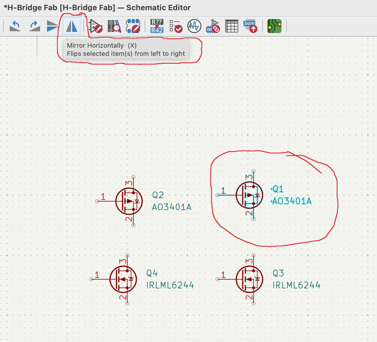
A really cool trick in KiCad is the ability to flip and rotate components, allowing you to position them exactly as needed.
To rotate a component, select it and press "R". If you need to make a copy, use Command + C and Command + V (on Windows, use Ctrl + C and Ctrl + V).
To flip a part horizontally, use Command + X (or Ctrl + X on Windows). You can also find these functions in the top menu if you prefer using the interface
instead of shortcuts.
This makes it much easier to position components so that their connections face the right direction. KiCad has many useful hotkey functions, but there
are too many to list here!
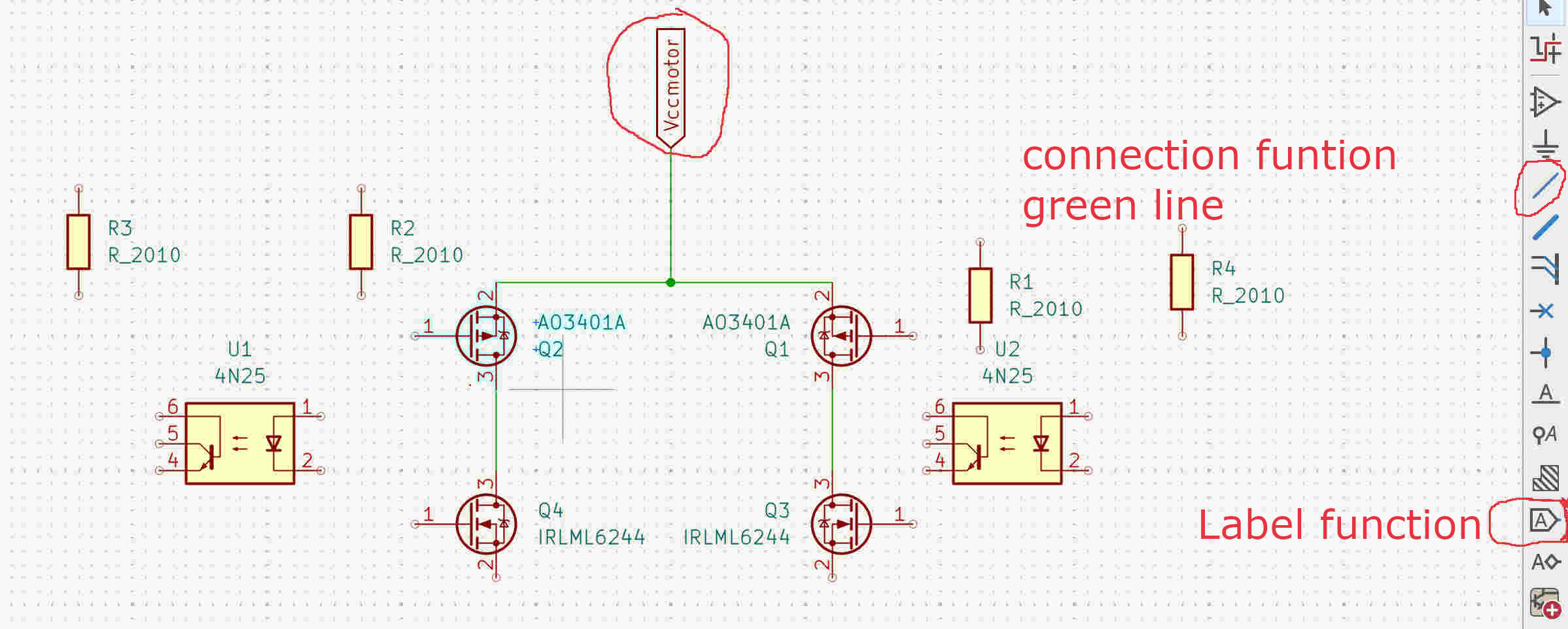
My personal recommendation is to lay out the components as planned on a sheet of paper or based on their setup on the breadboard. This makes it much easier to follow the layout.
Here, all the components have been arranged, and a Label has been added. Labels are useful for connecting components located on the same sheet or even across multiple sheets.
In this schematic, the label will be used to connect to a pin header later, signaling to the software that there is an external connection.
To create the green lines, use the Draw Wires function, which can be found in the right-hand menu. This ensures that all components are correctly connected to the appropriate
inputs and outputs in the schematic.
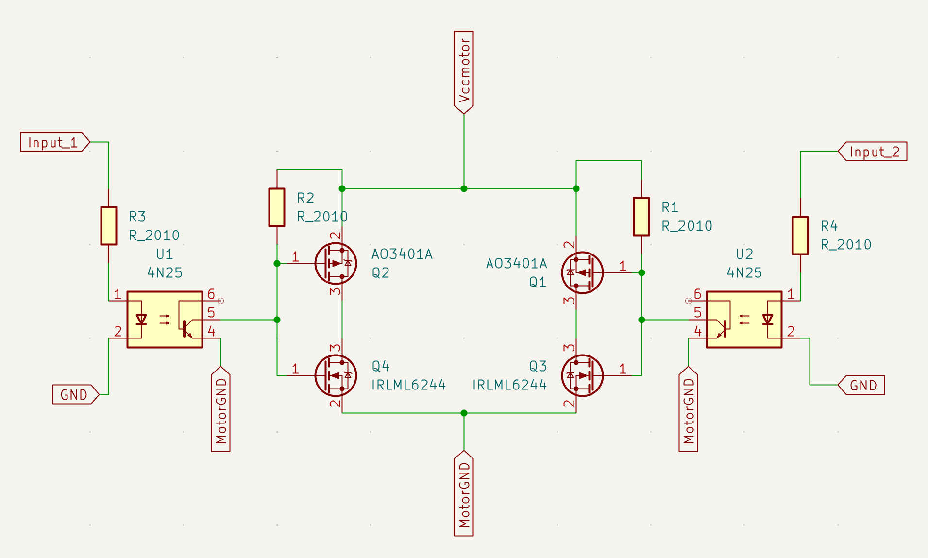
By now, all parts should be labeled and connected. The current result should look like this:
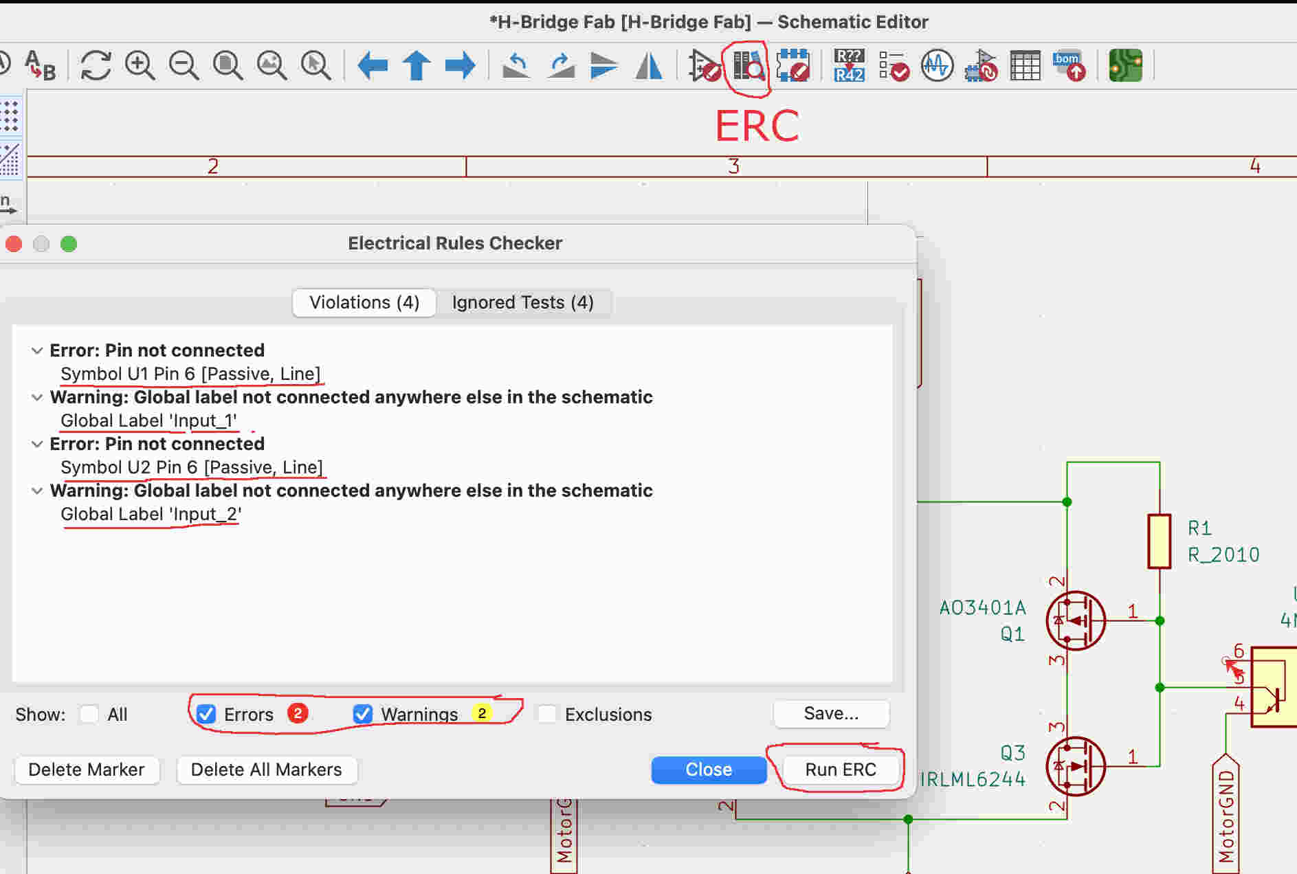
At this point, we should run an Electrical Rules Check (ERC). While this check cannot guarantee that the design will function correctly, it can detect connection issues,
such as unconnected pins or shorted power inputs and outputs.
To run the check, go to the top menu bar and select the icon with the books on it. In KiCad, this function is known as ERC. The diagnostics should run
automatically, but if they don’t, click the Run ERC button. This will display all warnings and errors found in the schematic.
If you right-click on a specific issue, such as Pin 6, you can choose to exclude it. In this case, it can be excluded because
it is not connected to any part of the schematic and is therefore unnecessary. However, other detected issues should be addressed accordingly.
The next step in the schematic is to resolve some issues while inevitably creating new ones along the way. Connectors were added to the schematic,
including the connection for the motor. This can be done using the Add Symbol button—simply type "connection" in the search bar.
A key reminder here is that not all parts in the library have an associated footprint, so you may need to add one later. If you plan
to use typical Arduino jumper wires, look for 2.54mm connectors, as this is the standard size.
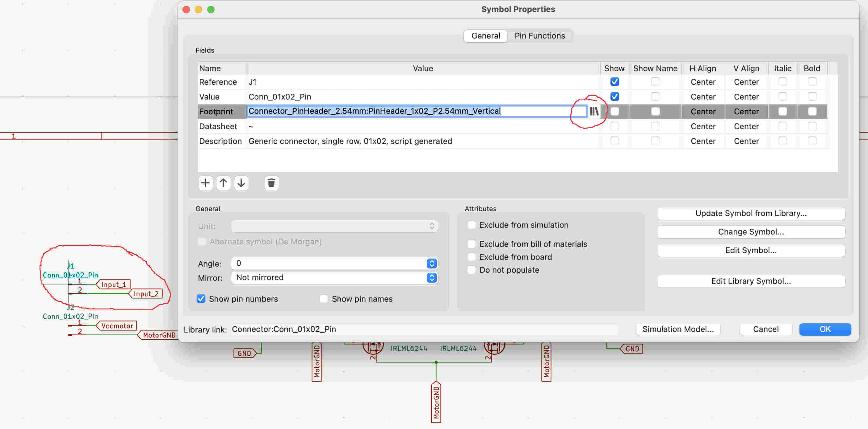
For example, if a footprint is not assigned when adding a pin header to the schematic, it can be added afterward. To do this, select the connector
or component, then double-click it to open a menu. In the image below, the footprint has already been added. To change the footprint, click on the
book icon, which will take you to the footprint library. From there, simply select the footprint you need.
The current state of the schematic should look like this after adding some connectors and a DC motor. The DC motor here is just a symbol and I will remove it as we dont need the motor on the PCB board, we just need connections. Here you can delete the symbol of the DC motor and add two connecter and label them M_Out1 and M_out2.
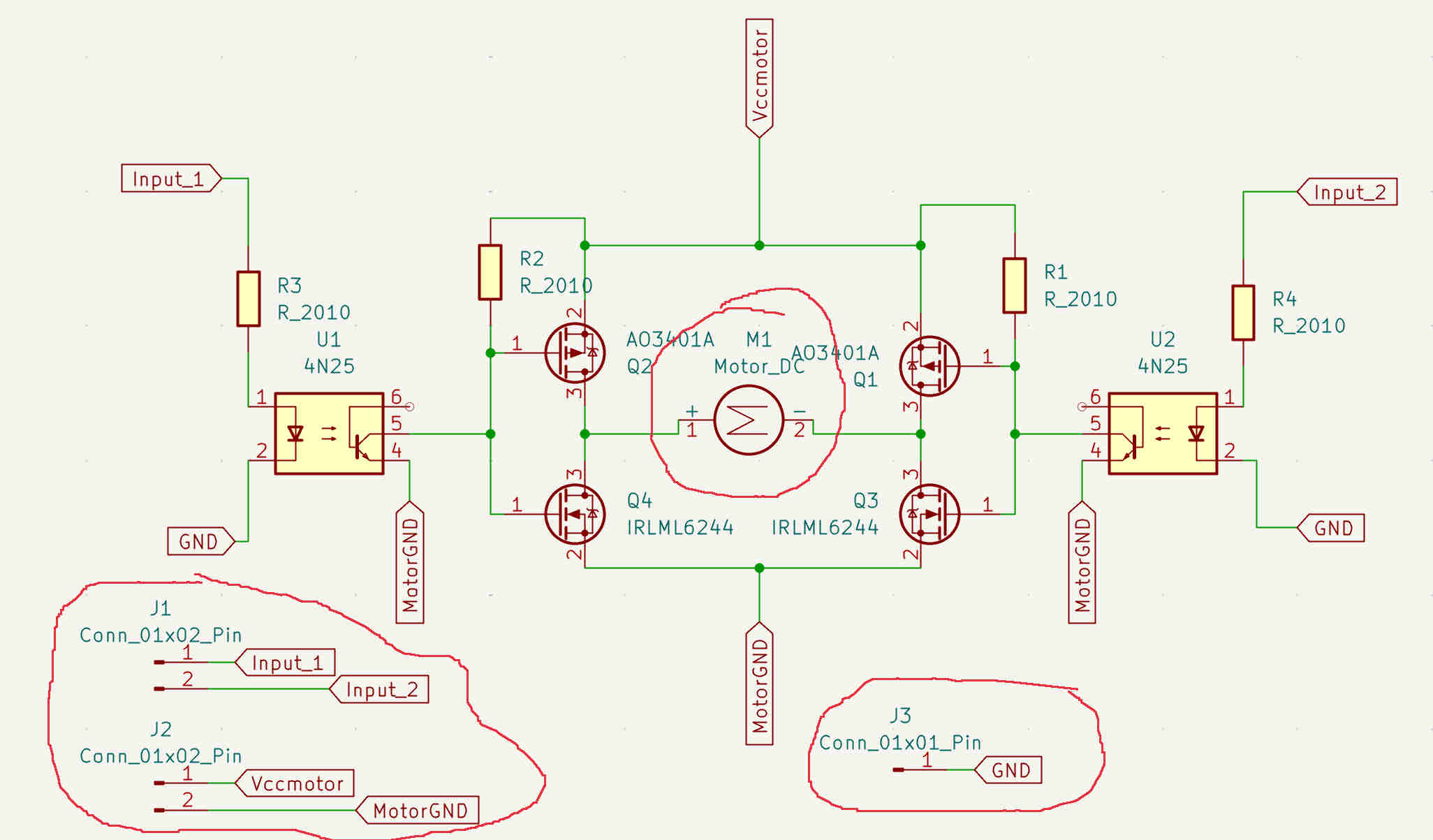
This should leave you with a completed schematic with all connections and footprints.

PCB Editor
Now that the schematic is complete, we can convert it into a PCB by generating a Netlist file. First, go to File > Export > Netlist... and save the file in the same project folder as the schematic.
Then, open the Home window in KiCad, select PCB Editor, and go to File > Import > Netlist.... This will import the schematic’s footprints into the layout.
At first, the components will appear with crossing lines, representing the electrical connections from the schematic. In the menu that appears, the top-left corner displays
the component footprints, and there is also a window where you can update any changes made to the schematic. If modifications or additional components are needed, the Netlist
must be exported again, re-imported into the PCB Editor, and updated.
Organizing the components properly makes routing much easier. Having two screens open—one with the Schematic Editor and the other with the PCB Editor—is highly recommended.
This helps when reconstructing the circuit and locating specific components. If a part is hard to find on the PCB, selecting it in the Schematic Editor will highlight it in
the PCB Editor, making it much easier to work with.
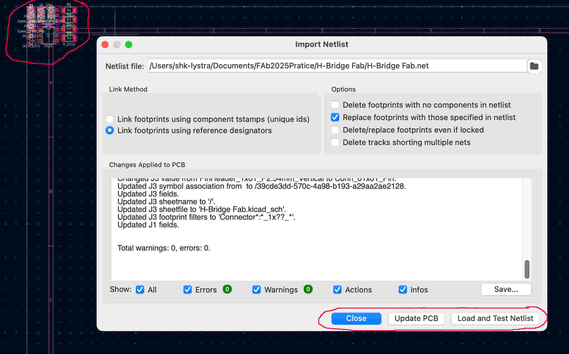
Laying out the part to be able to tell them apart from on another
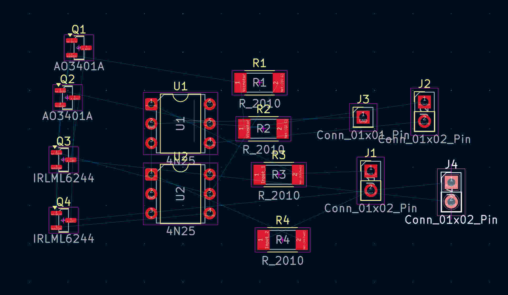
Next, it’s time to focus on the board layout. If the board is being manufactured by an external company, using multiple
layers is fine, as it allows for shorter and more efficient routing. However, since this board will be CNC-milled, it
will be made on a single-layer copper plate, which makes routing more challenging.
For this board, it took several attempts to rearrange routes and components to find the best placement. Initially, I struggled
to connect two routes properly—it felt like solving a maze. But once everything clicked into place, it was incredibly satisfying.
The routing lines help guide you toward the paths of least resistance. Additionally, it's best to avoid 90° angles, as they can make
machining more difficult.
The next step was to copy the layout from the schematic. Then, I added an edge cut to define the working area, creating a border and set
dimensions to work within. This part was straightforward. Since this is a PCB, the layout can be arranged with all pin headers on one side
and all resistors on the other. To connect the components, open the right-side menu bar and select F.Cu to route on the top layer or B.Cu to
route on the bottom layer. The same menu also includes the routing tool for creating the necessary connections.
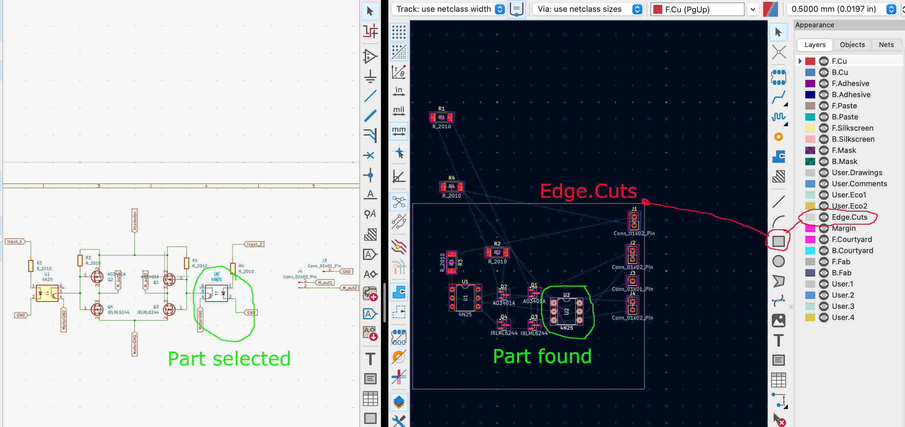
At this point there are still two layers. In the worst case one could just solder in a wire. Another solution would be to add either jumpers or zero Ohme resistors.
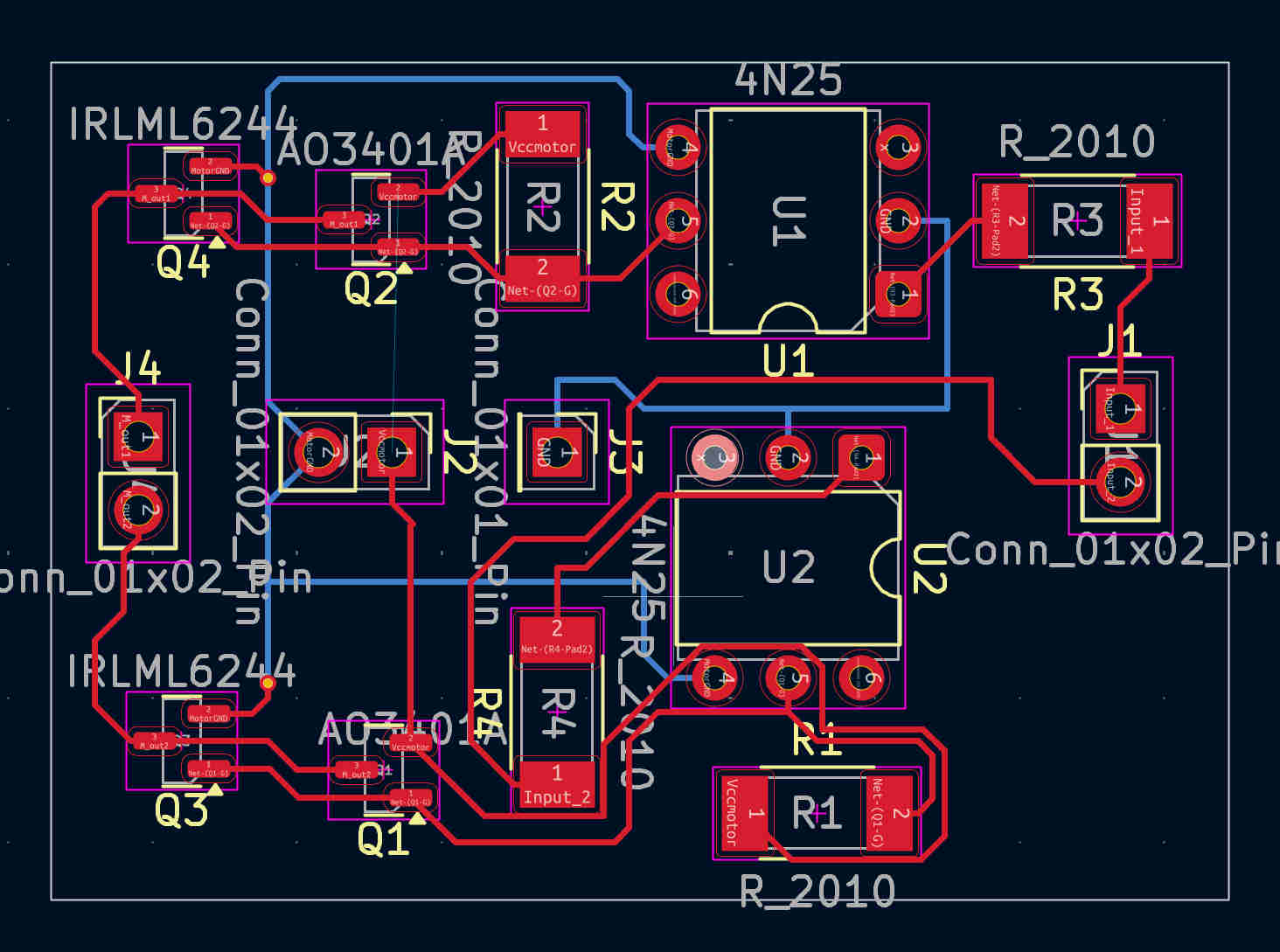
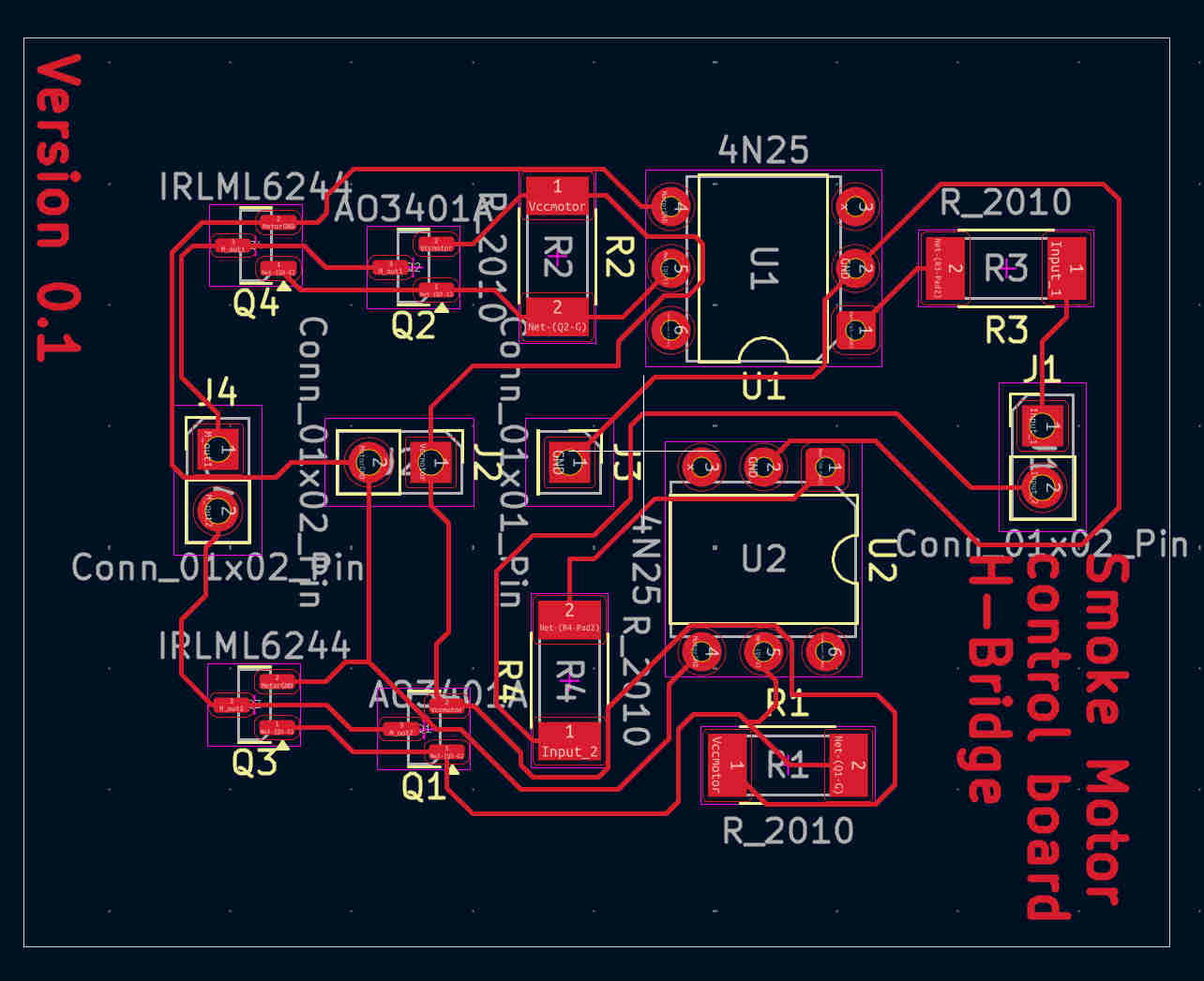
After play around and really trying to find a route that would allow for a all connections to be on one side. This involved moving routes around and reshaping them I found a the paths I was looking for and the here is the end result.
Gerber Viewer
Now that the layout is complete and all the paths have been connected, we can add the filler zones. On the right-side menu, you will find the function that allows you to draw a border around the cut edge. In the pop-up menu, select GND to connect all ground traces. This does not include the motor GNDs—only the main GND. Since there is only one layer, select F.Cu.
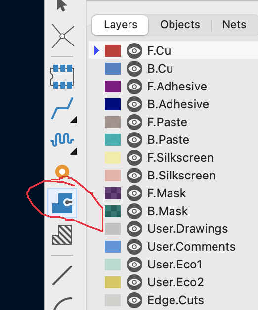
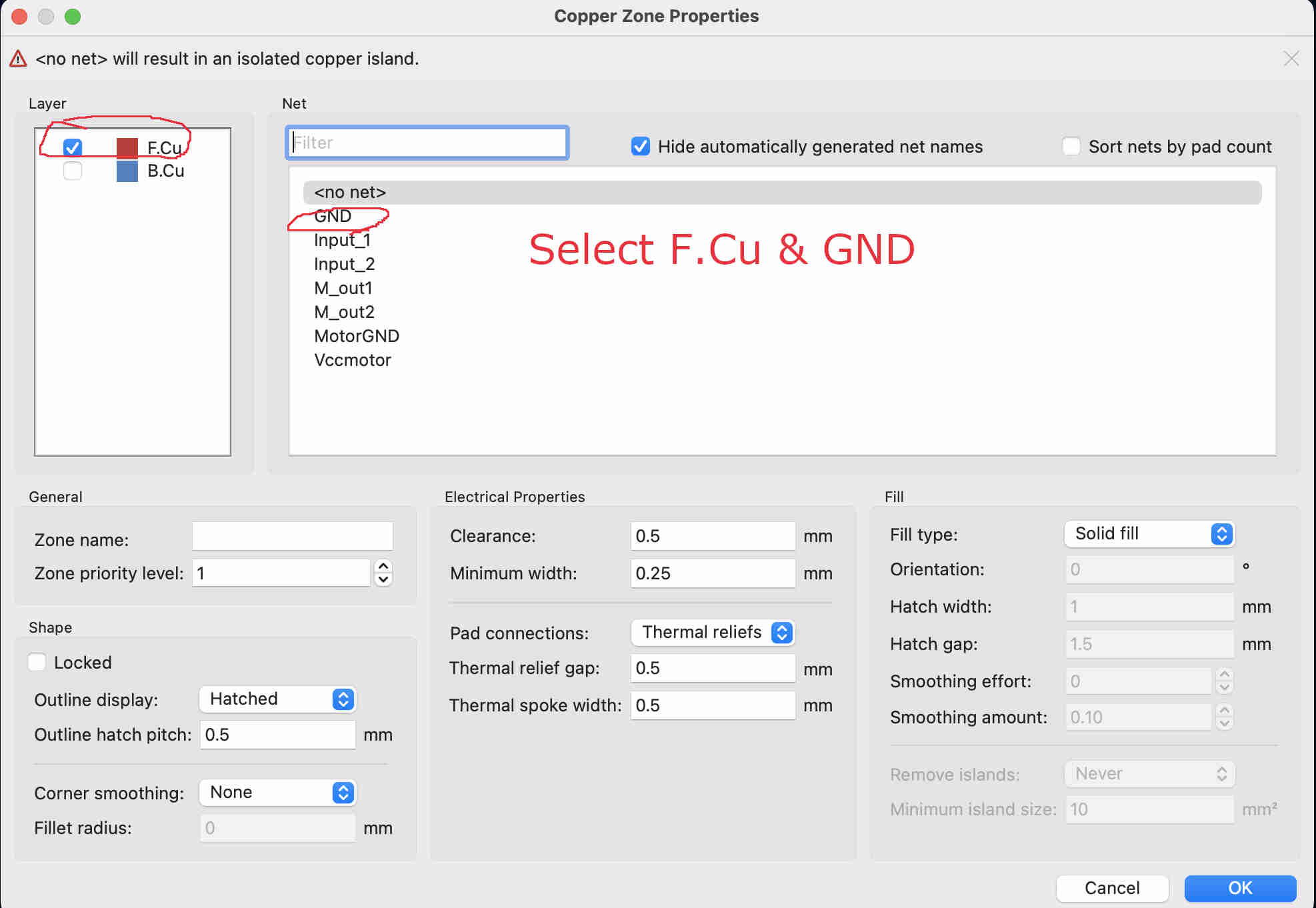
This will create a copper infil, where the left over copper is GND. Result after running along the edges of the PCB out line should look like this:
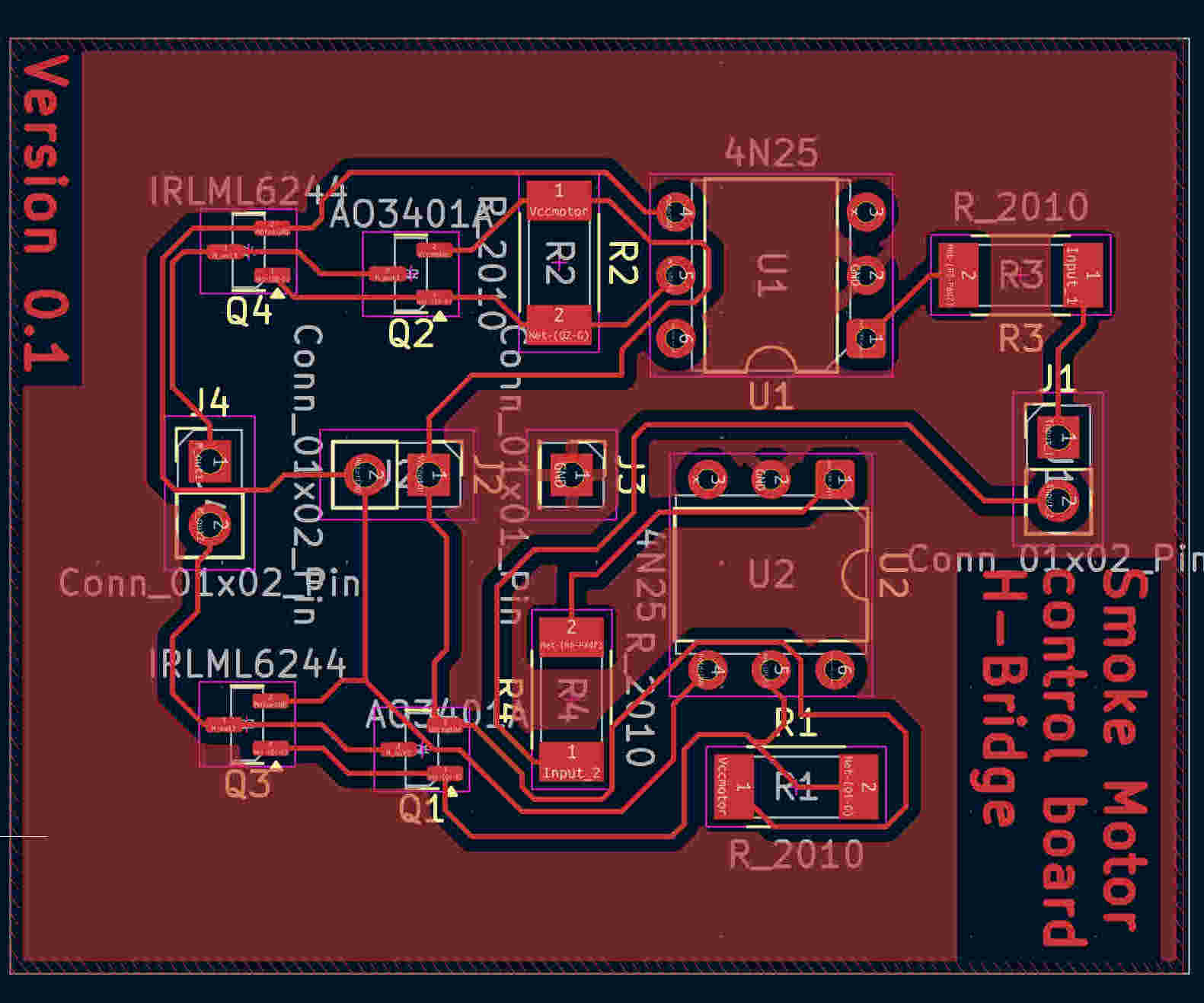
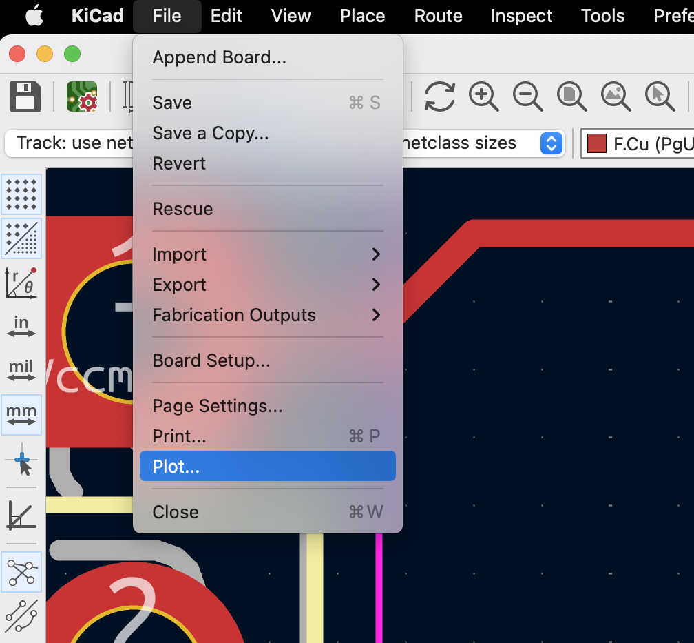
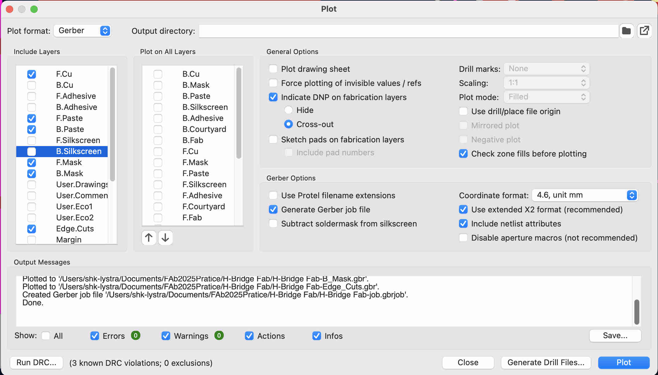
The next step is to generate a Gerber file. To do this, go to File > Plot. Here, you will find various options depending on the number of layers and other features your board may have. This process will also run a check for any potential issues, such as duplicate routes, unconnected pins, and other errors. Once all errors have been resolved, run the check again to ensure nothing was missed. If the board is going to be professionally manufactured, you may also want to add elements such as screen prints. An alternative way to generate a Gerber file is by going to File > Fabrication Outputs > Gerber Files.
Click here to download the files.
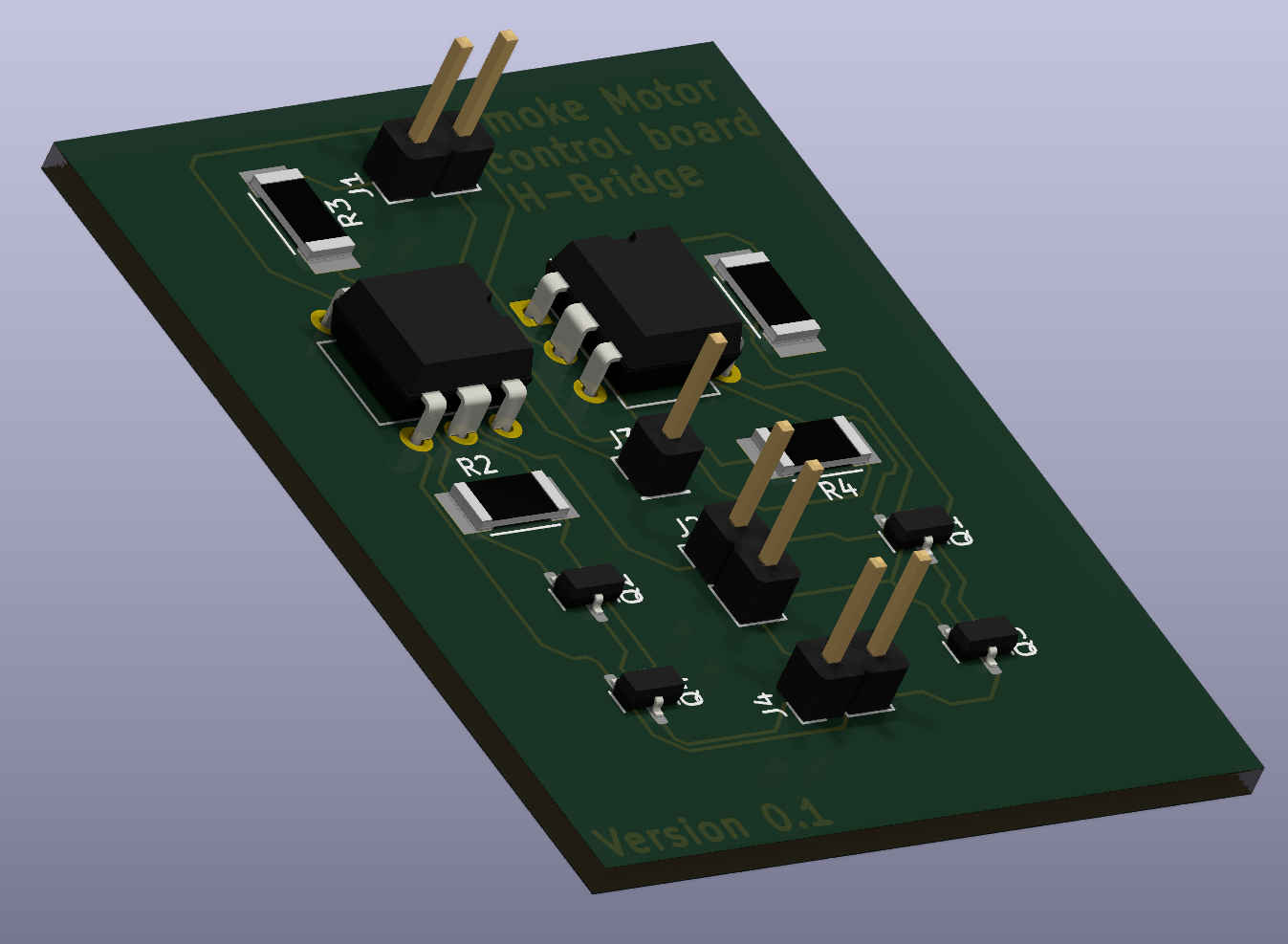
Hero Shots

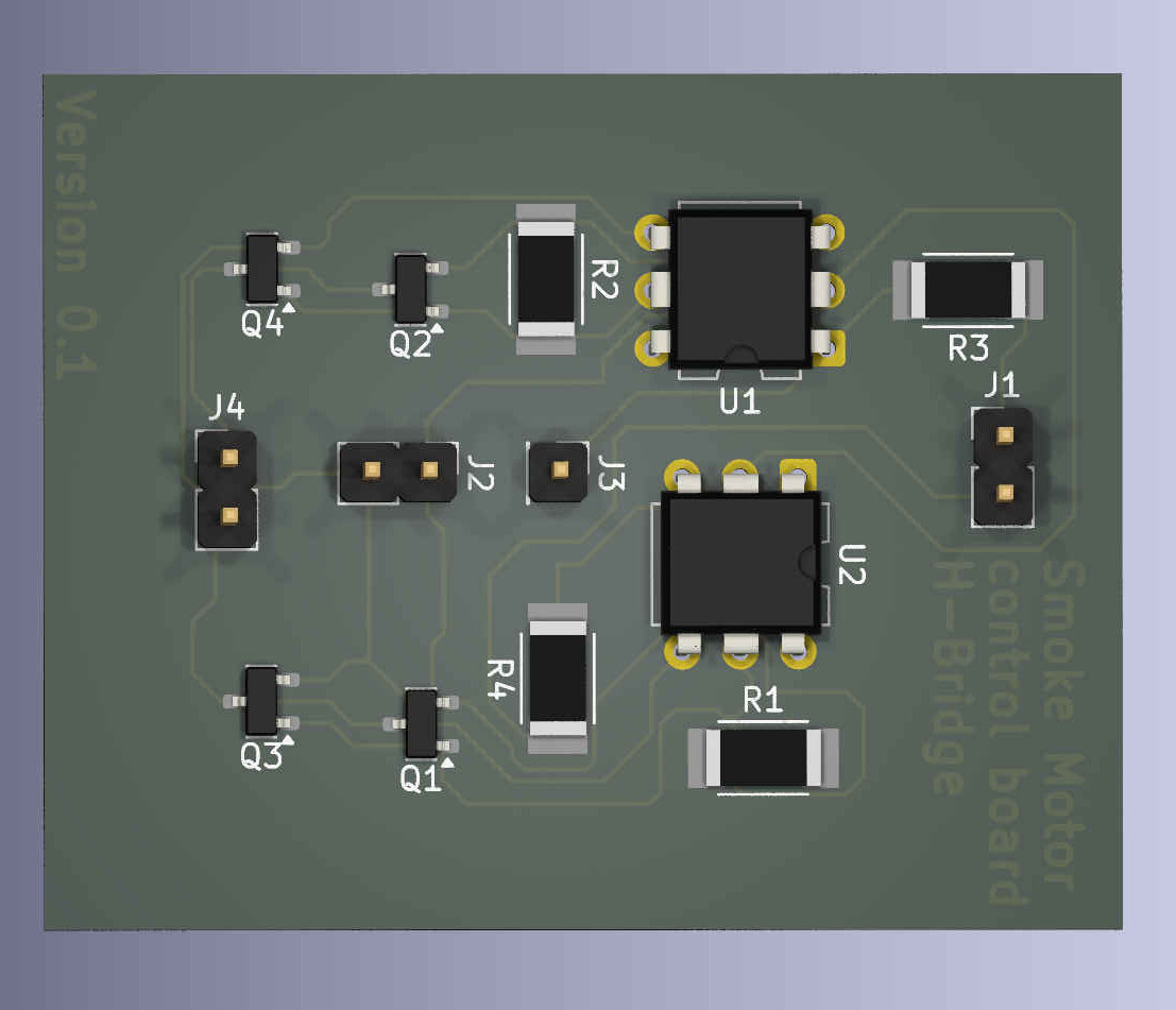
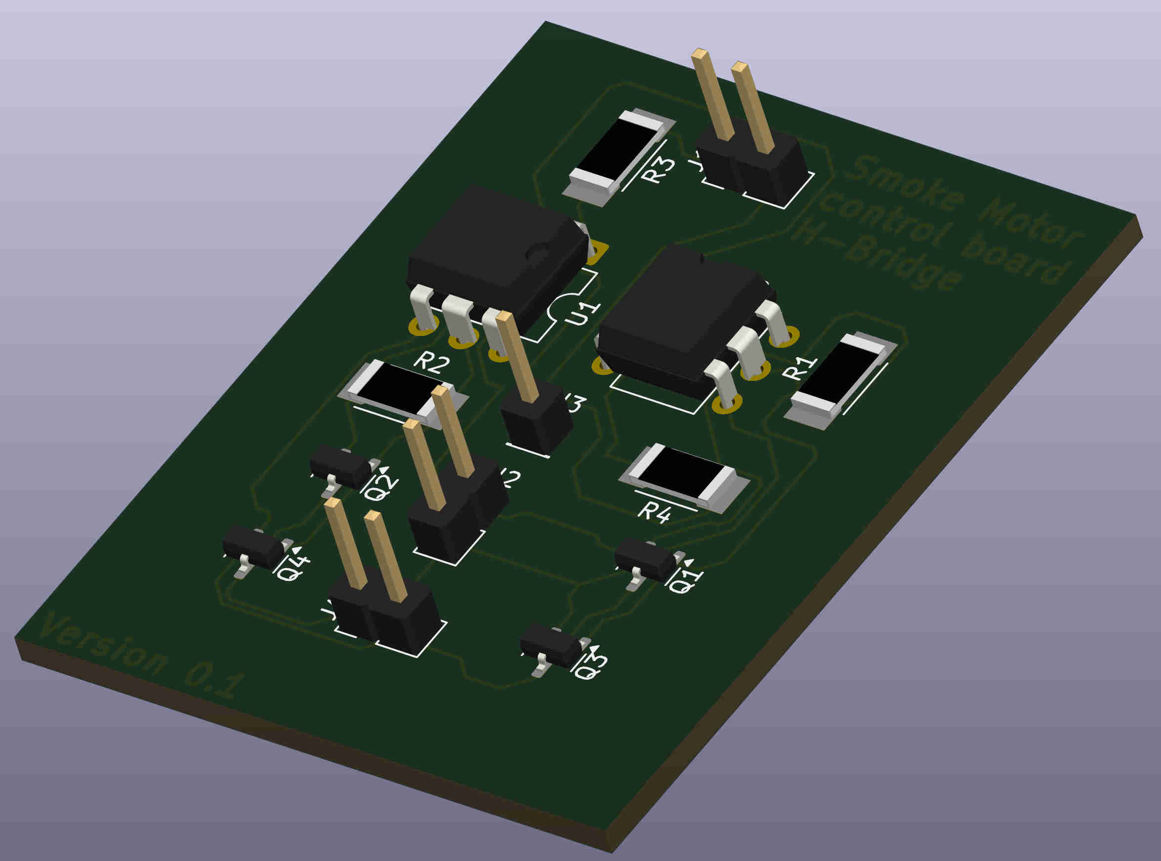
What the board does
This board is part of my final project and will be used to control a small DC motor to help blow smoke through a small pipe over an object, demonstrating how air flows around the object and where turbulence may occur. The DC motor can now be controlled by a micro-controller like the ESP32 or other similar boards. As mentioned above, a DC motor cannot be directly connected to a micro-controller, as it would burn the board. The H-bridge will receive a PWM signal, allowing it to control the DC motor without any issues. The motor itself will have an external power source, which will be regulated with the help of the H-bridge and the PWM signal.
I missed a bit of information
Lets do this again, misunderstood the assignment. It happens. We were supposed add a micro-controller to the board design. I understood that the board had to be able to communicate with a micro-controller, which the board does. I am left with two options either link you to the assignment Electronics Production or add a micro-controller to the current. Now that I know what I am doing, I can just open the design in KiCad and add a micro-controller. This is fairly simple find the board you want use and add the connection. Here a RP2040 from the Fab library was used and a couple extra pin outs were added for the case that more components can be controlled to the the board. Click here to download the Gerber files. Not to forget the data-sheet for the RP2040 pinout. The Rp2040 will be regulating the PWM signal to the Motor. It will also supply the voltage needed to for the small DC motor. Down below you will so see the schematics for the this set up.
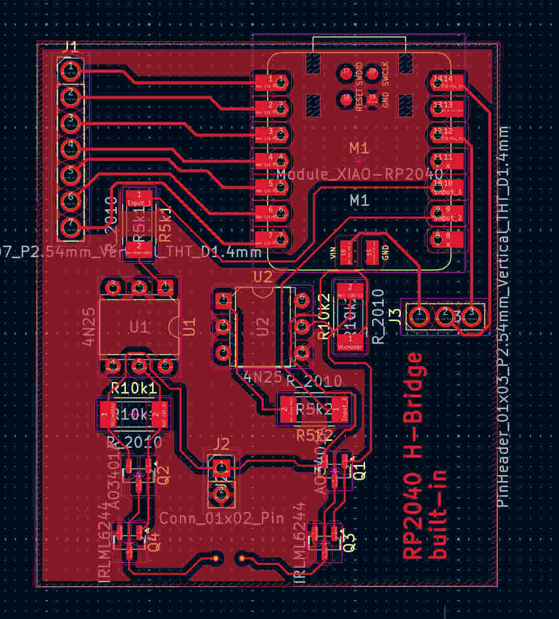
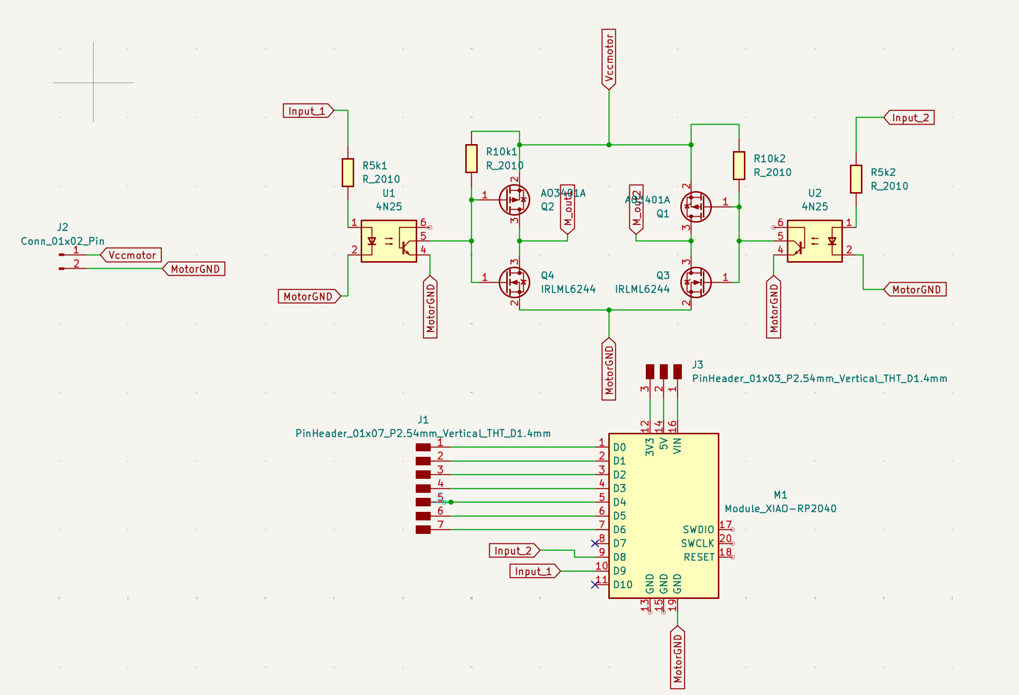
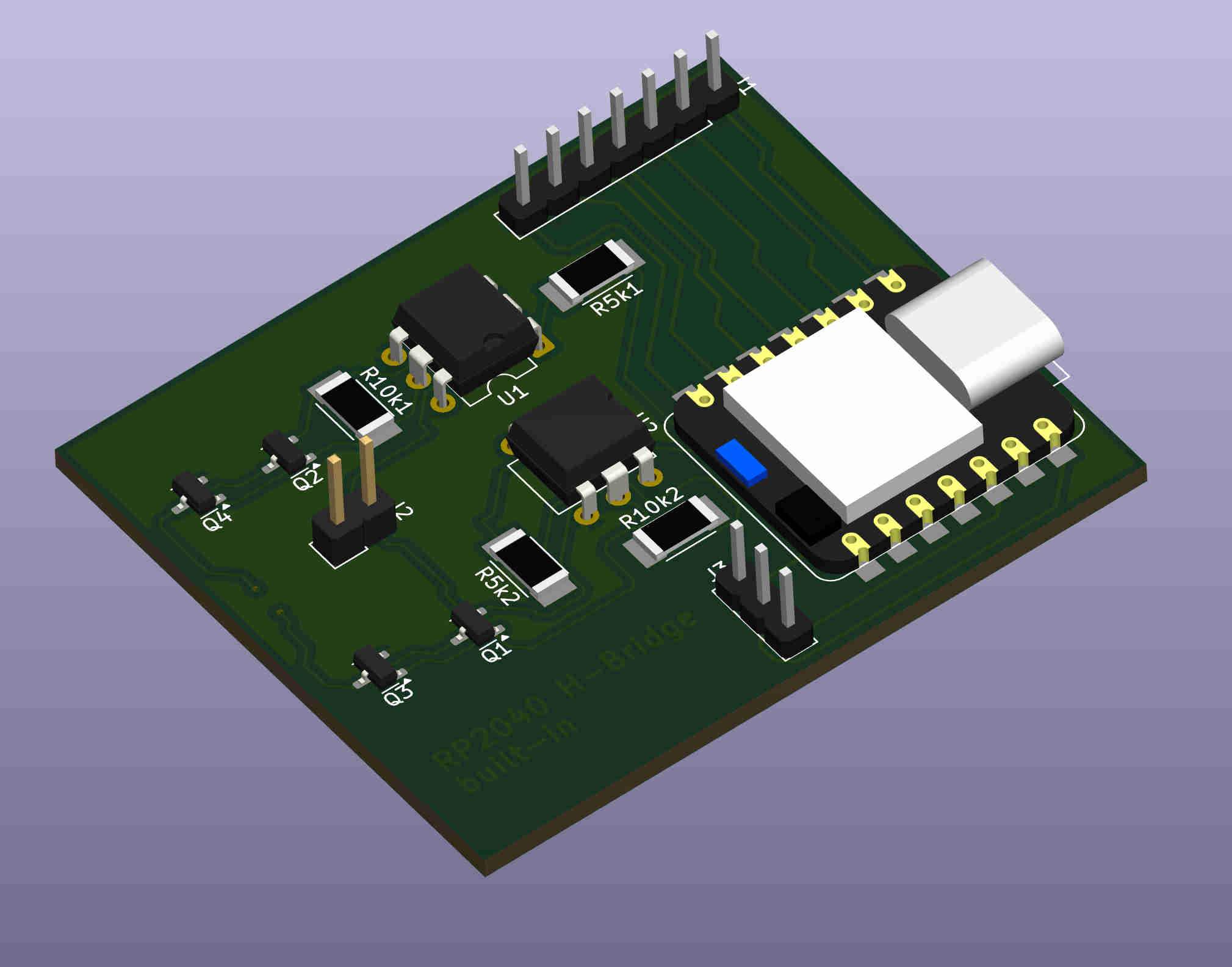
Final Hero shot of the H-Bridge RP2040
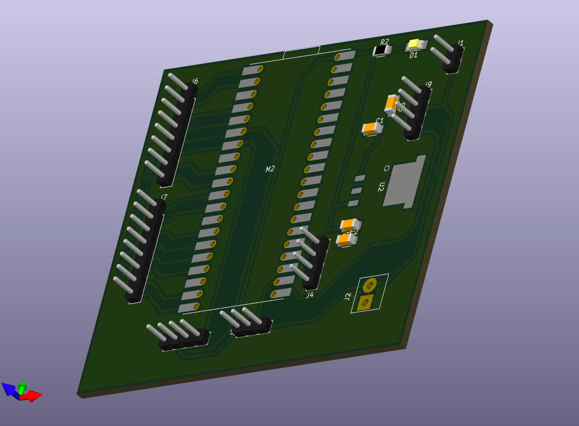
Raspberry Pi Pico Integration Board
This PCB was designed and created during Electronics Design. You can download the ZIP files here.
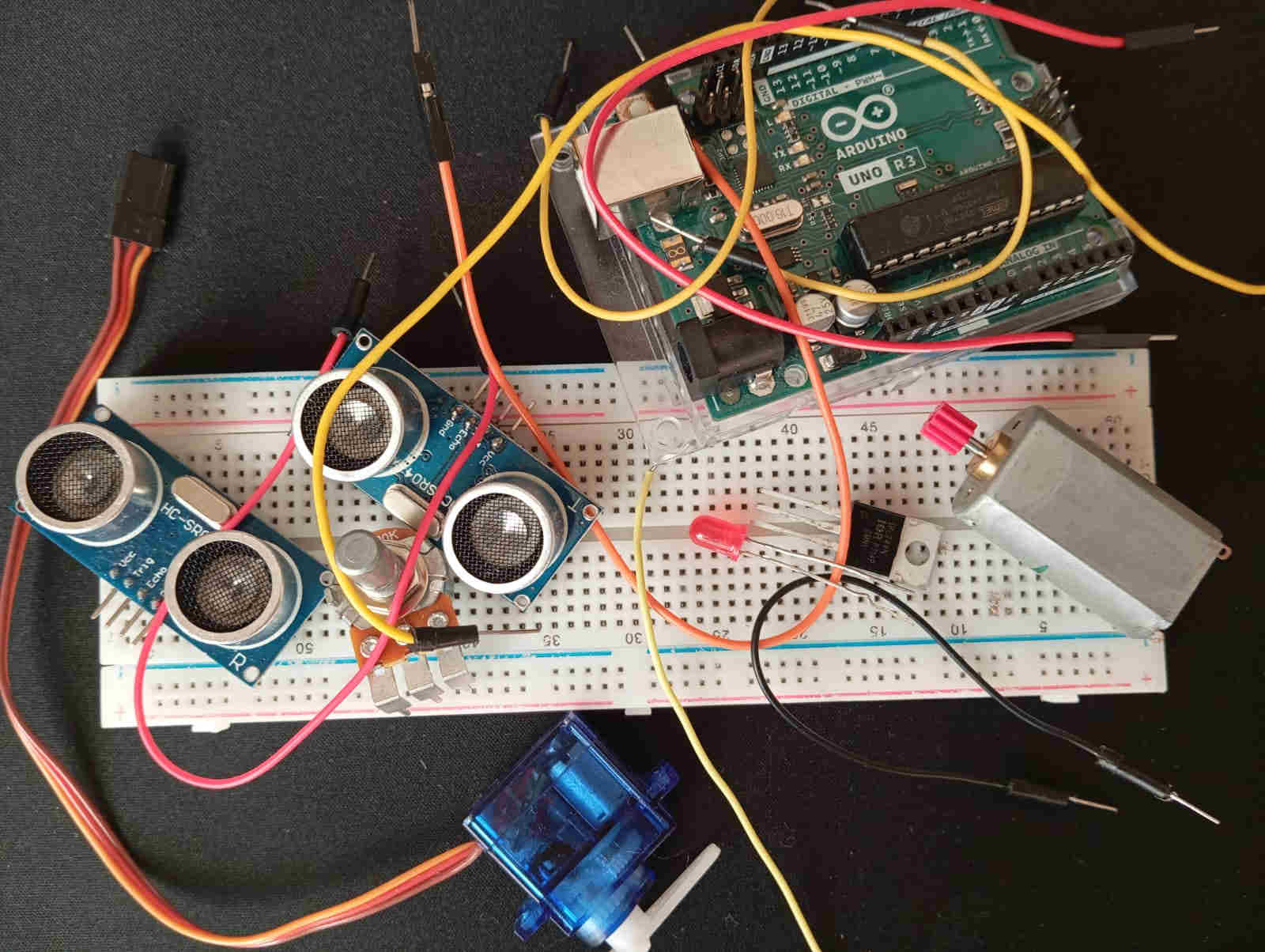
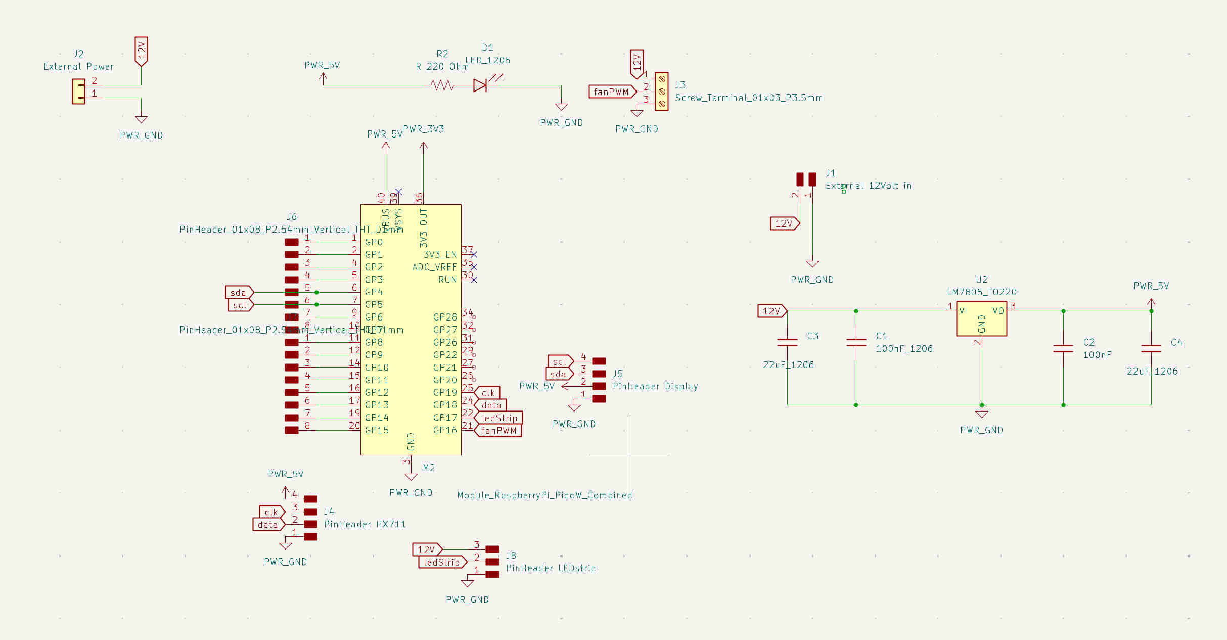
After burning my first Arduino — and yes, it really does stink when that happens — I learned an important lesson: always double-check your ground and positive connections. The second lesson? Always verify your setup with a voltage meter before connecting anything to a microcontroller. This mistake was a tough one, but it taught me a lot. I realized I'm much more comfortable with mechanical systems and should ask for help when it comes to electronics. Still, I’m not one to give up easily. With my instructor’s guidance, I managed to design a board that includes: extra pins for future updates, a 12V external power supply, a 12V-to-5V voltage regulator, an LCD screen, LED lights to backlight the tunnel, a load sensor to measure lift or pressure on an object, and a connection for the PC fan.
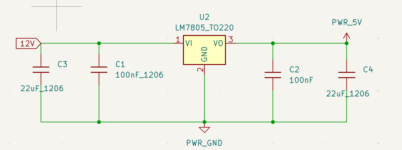
To create the PCB, I used KiCad, which we learned during the Electronics Design assignment. After making a list of the parts I wanted to include, I checked their datasheets and began placing the components, starting with the Raspberry Pi Pico. Since the board would be powered externally, a voltage regulator was needed to step down the voltage. This would supply power to the Pico, the LED strip, and the fan. The voltage regulator circuit includes four capacitors (two 22uF and two 100nF) and an LM7805_TO220 — a 1A, 35V linear regulator that steps the voltage down from 12V to 5V.
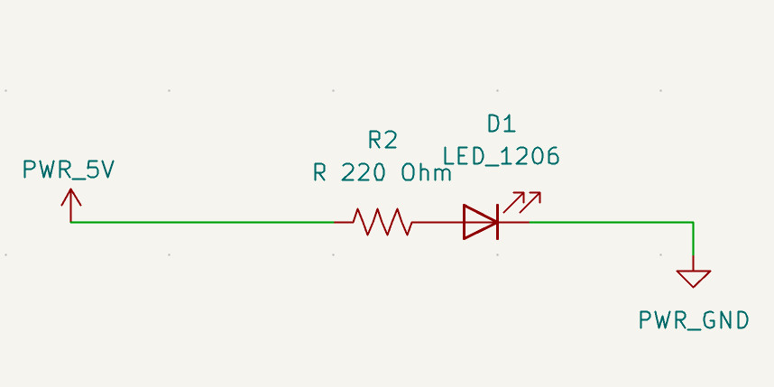
Next, I focused on the Raspberry Pi setup. Reviewing the datasheet, we noticed that the Pico does not come with a built-in LED to indicate power status. To fix this, I added a 200-ohm resistor and an LED, connected between the 5V supply and ground.
When it came to choosing an LCD screen, I explored options from az-delivery.de. Since no datasheet was available for the screen module I selected, I relied on the pinout labeled directly on the module to figure out the necessary connections to the Pico.
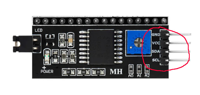
After identifying the required connections, I added a 4-pin header and made the corresponding connections on the board.
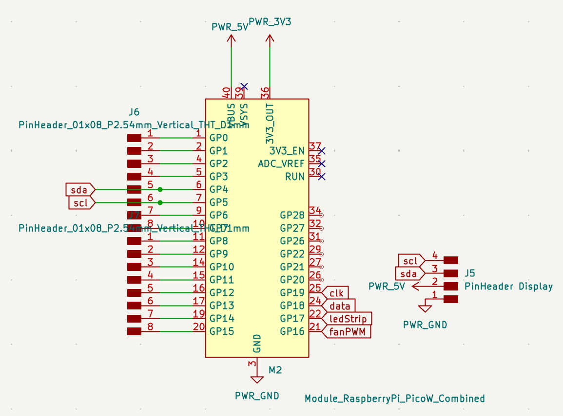
Since this board might evolve in the future, I also included extra pins. Once you know what you’re doing, the full schematic layout becomes quite straightforward. I'm excited to keep learning — designing custom PCBs really cleans up your projects compared to using prototyping boards and tangled breadboards. I hope this PCB will make my final project look much more professional. Below is an image showing the current full schematic setup:
Setting up the PCB
Setting up the PCB layout depends on how you want the board to function. I chose a simple, organized layout, placing the external power supply connections on one side of the board and all other components on the other side. This design keeps the wiring tidy and makes it much easier to find and connect everything properly.
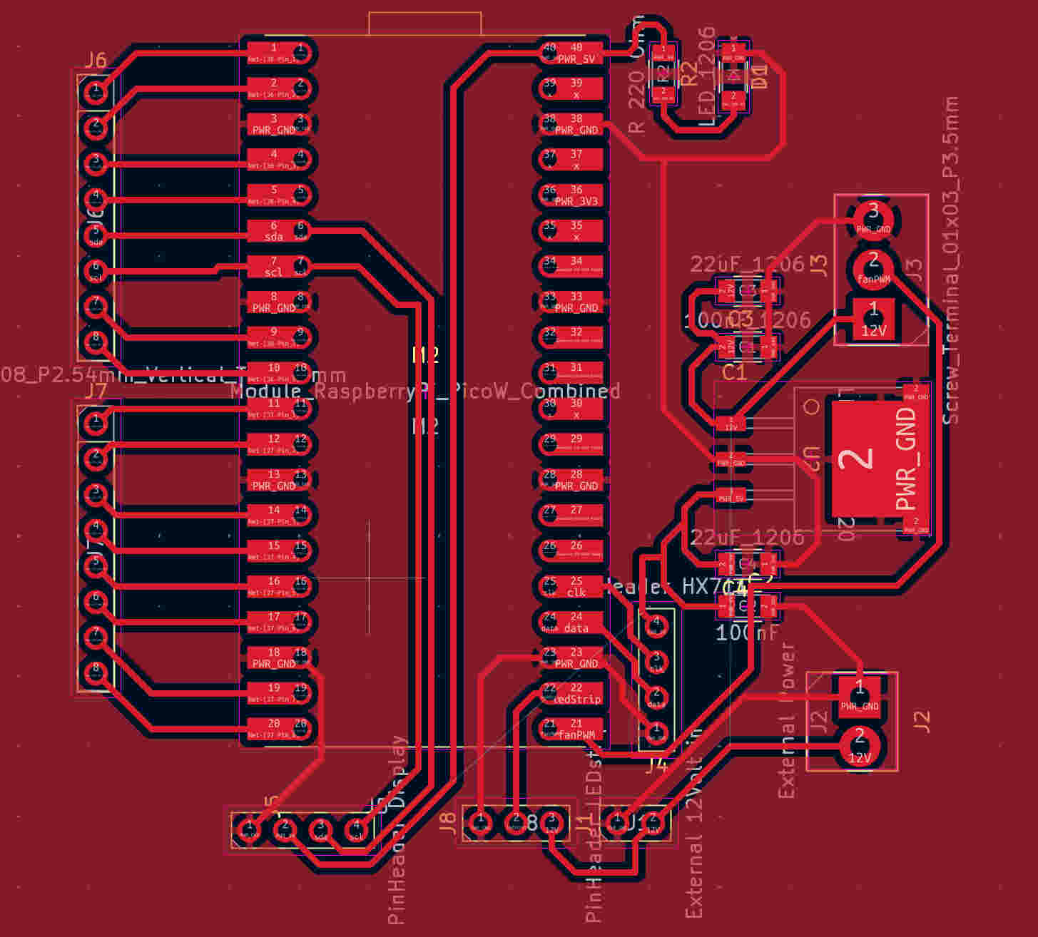
Hero shot of the PCB
