Week 08 - Electronics production
Goals
group assignment:
- characterize the design rules for your in-house PCB production process
- extra credit: send a PCB out to a board house
individual assignment:
- make and test the development board that you designed to interact and communicate with an embedded microcontroller
- extra credit: make it with another process
Week's explorations and achievements
- I had no prior experience with electronics production, except from soldering.
- I designed a second development board because we were missing some components that were supposed to be on the board I designed during week 6 - Electronics design (they were ordered but not yet recieved)
-
I used 2 different techniques to create my PCB's tracks:
- Milling a bakelite board covered with copper to isolate copper tracks, using a Roland SRM-20 CNC milling machine and cylindric mills
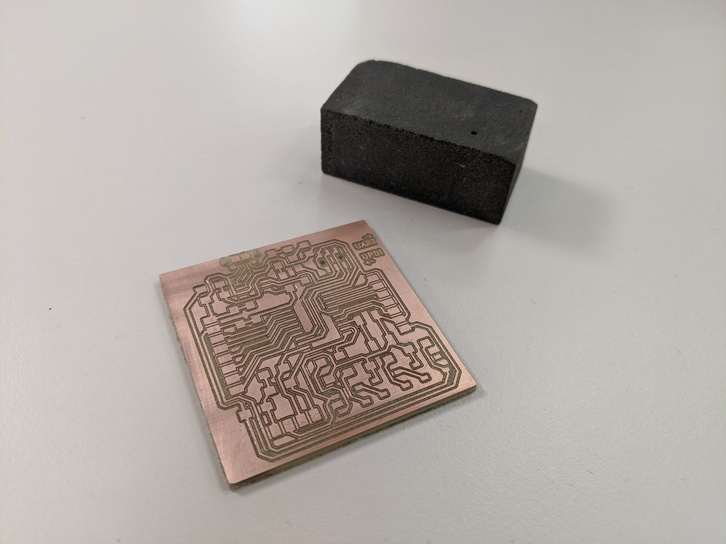
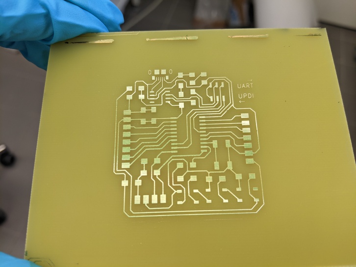
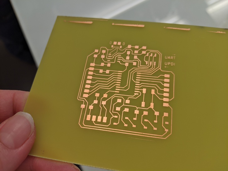
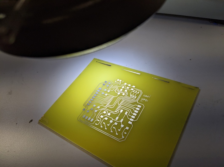
- Chemical etching using a garolite board covered with copper and UV reactive resin, a mask printed on a transparent plasti sheet, a UV insoler, perchloride iron, and acetone. I also tinned the tracks with a tinning solution homemade with tin salt and HCl.
-
I varnished one board using UV reactive varnish, a UV insoler and the laser cutting machine to etch the pads
- I did the hand soldering of the surface mounted components for one of my boards
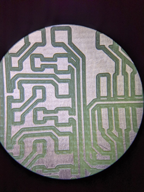
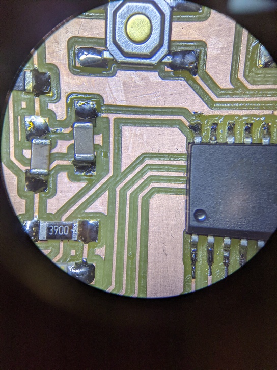
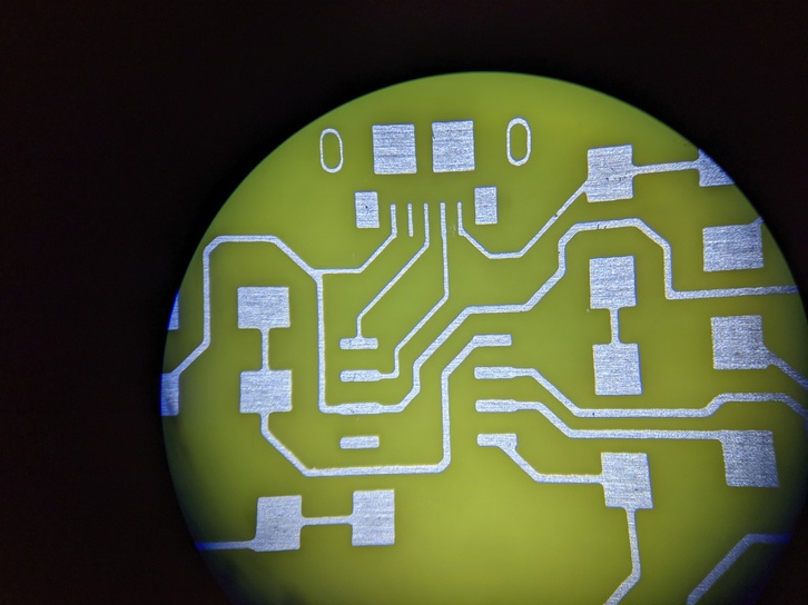
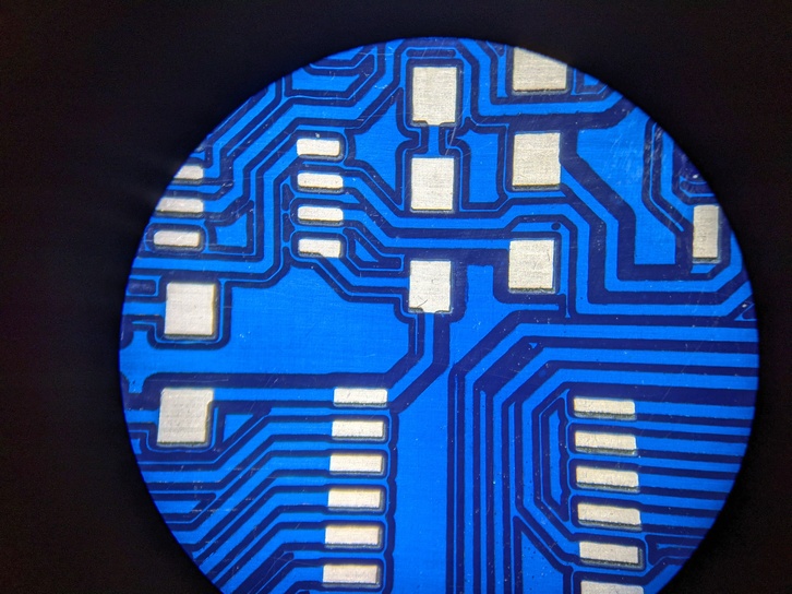
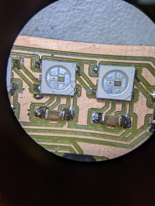
Here are some pictures of the boards taken through the binocular magnifier:
Group assignment
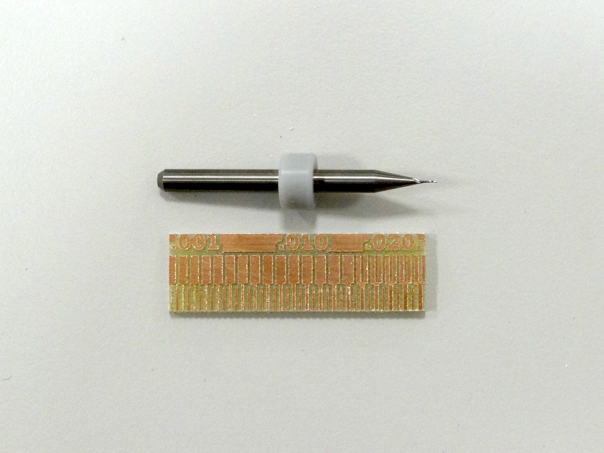
This week's group assignment was about finding limit values for our milling machine. I used the file provided by the fabacademy to characterize these limits for a cylindric 0.4mm mill. It was the first time I used mods to generate paths for the milling machine, and I really won't carry on with this solution, which I found not explicit and specific enough - FlatCAM does a better job in my opinion on this exhaustive aspect.
KiCad Design
It's important to use a PCB making technique consistent with your design. If you go for milling, be very careful to the design constraints, such as the minimum distance between the tracks which must be consistent with the diameter of your mill.
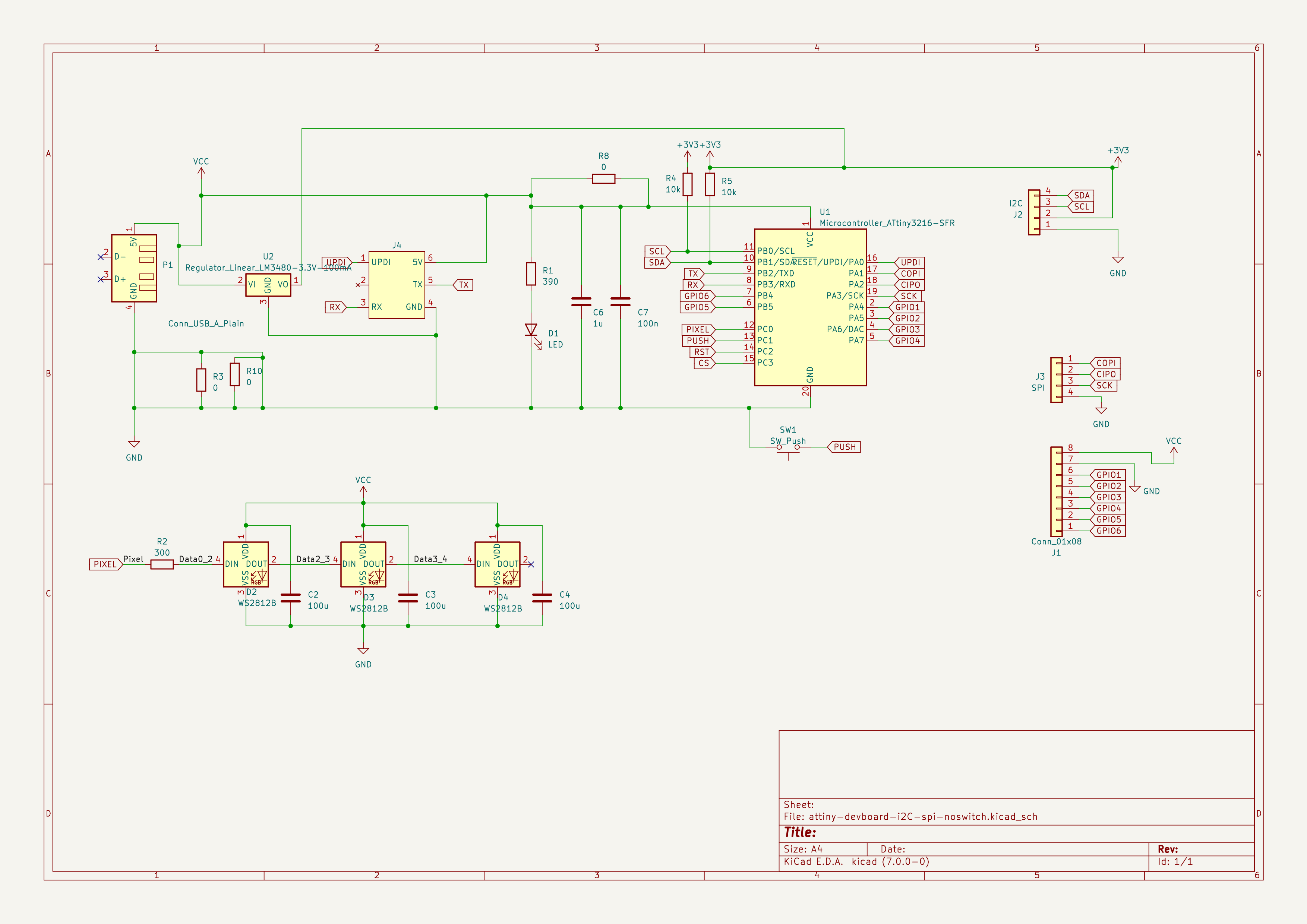
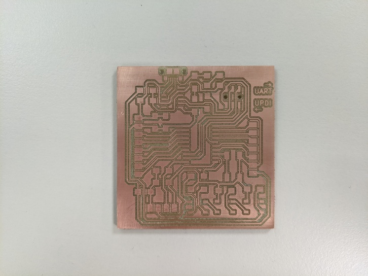
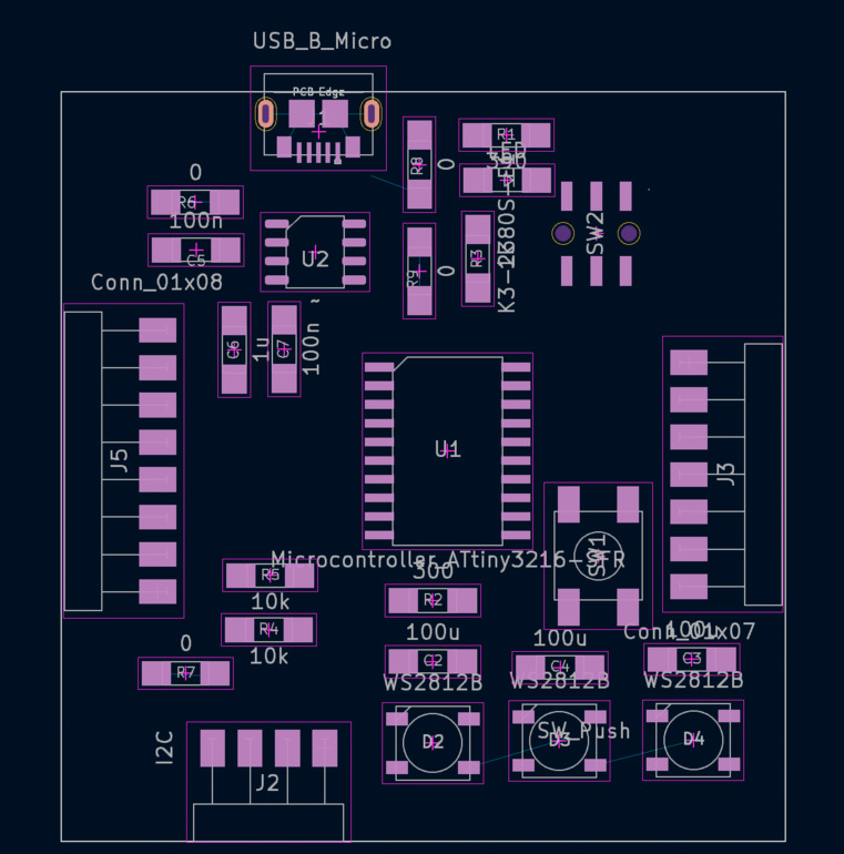
I manufactured two different designs, one made in the week 06 Electronics Design (you can find the files and screenshots in the corresponding week), and another simpler one, because I was waiting for some components to arrive (CH340N and switch). Here is the design of the simpler circuit without switch (you need an external UPDI programmer board to program it, USB is for power only)
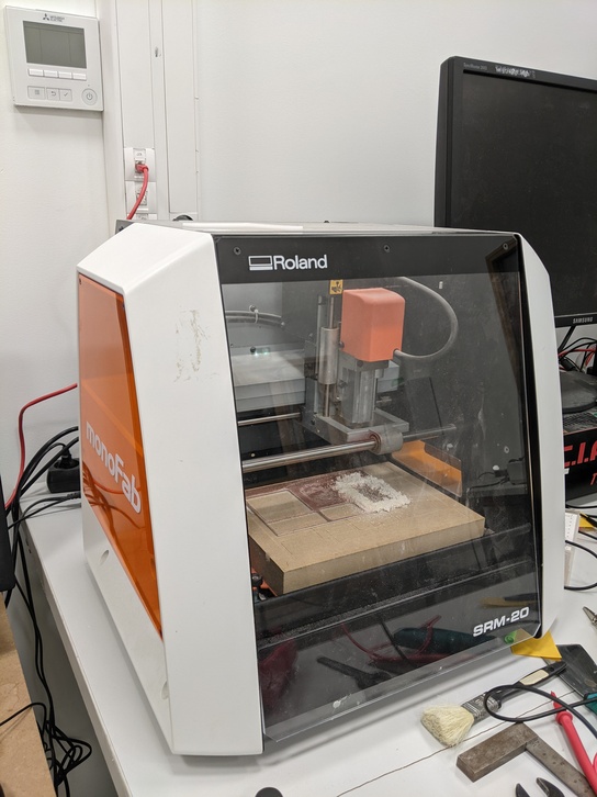
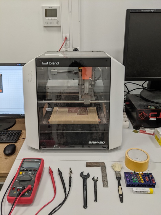
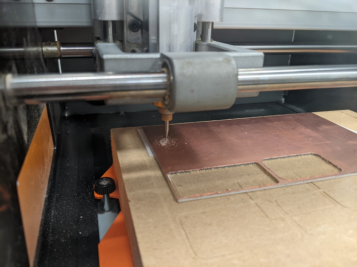
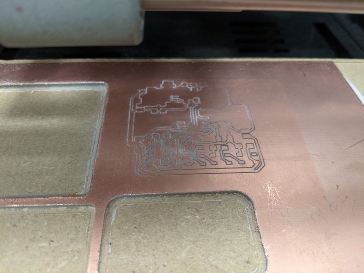
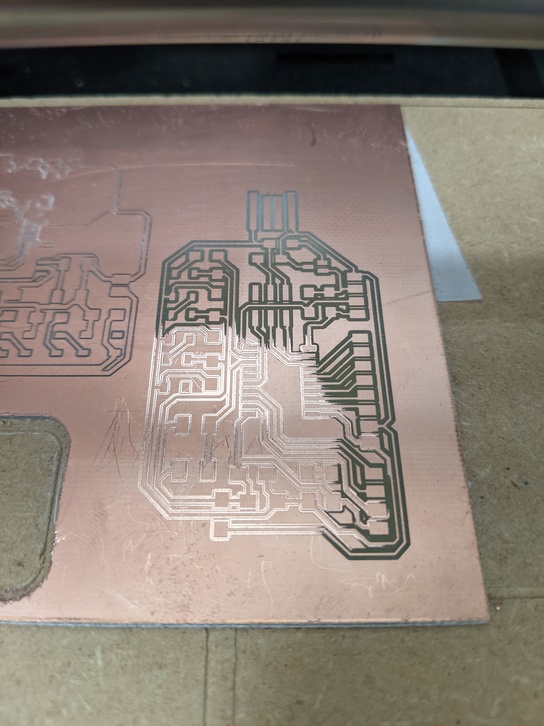
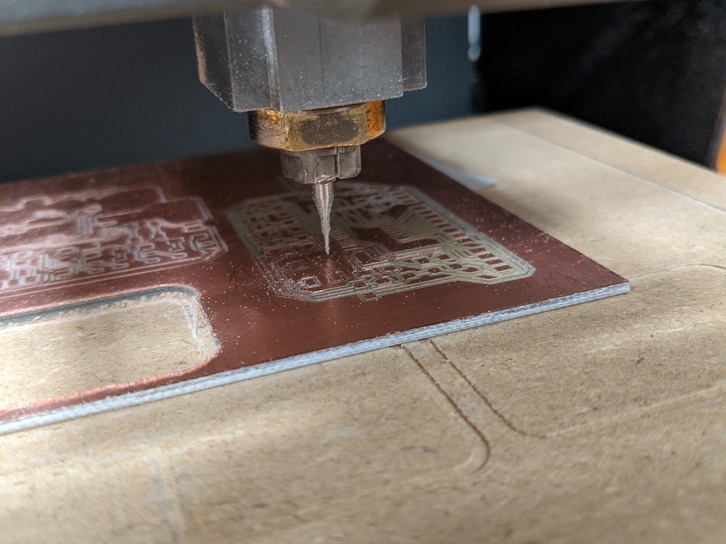
Machining with a CNC milling machine
Principle
This techniques consists in milling a rigid plate covered with a copper layer. The milling path isolates the different copper areas, thus creating copper tracks. It's possible to remove the copper from all the areas that are not tracks, but not mandatory. The sensitive part of this technique is :
- the design rules of the PCB must comply with your tool's diameter, in particular if you're using cylinder mills
- you need to have the flattest surface possible and zero you tool numerous times, as the tool is very sensitive to height variation: you can either break the mill, or mill isolation path with inconsistent width - or even an isolation path that does'nt go all the way through the copper and thus doesn't isolate tracks.
We'll only focus on single-sided boards.
Material
Machine
We'll use the Roland SR-20 monoFab compact milling machine. The maximum spindle speed is 8000 rpm.
Tools and material
- Mills
- 0.2, 0.3 or 0.4mm diameter cylindric mills to cut the tracks of the F.Cu
- 2mm diameter cylindric mills to cut the edge of the board
- Drills
- I needed a 0.4mm drill to place the USB port and the switch
- Board material
- We used fr4 bakelite boards, 1.8mm thick : the medium is made of bakelite with a 0.035mm thick copper layer (this value is stated by the vendor but can probably vary from one board to another)
Also make sure to have around you:
- Double-sided tape
- A multimeter to level the Z
- A vacum with a filter
- Respiratory masks
- A brush to remove the dust
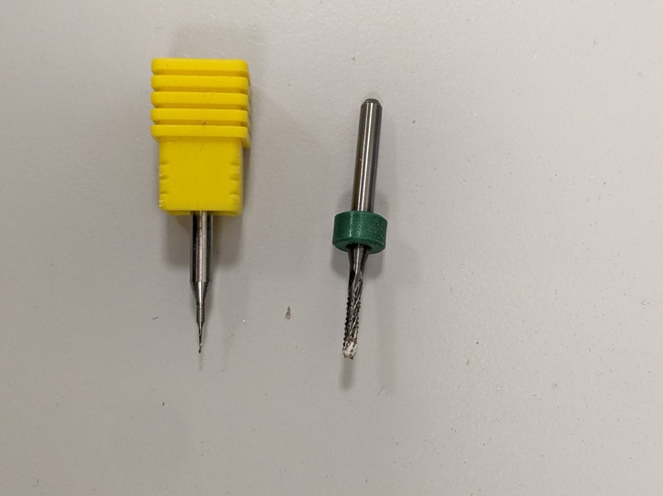
0.4mm cylindric mill and 2mm cylindric mill
Speeds and feeds parameters
Here's the speeds and feeds parameters for cylindric mills that our instructor provided us and which I used:
| Diameter | Cut Z | Feedrate X-Y | Feedrate Z |
|---|---|---|---|
| 0.8 mm | -0.06 mm | 120 mm/min | 100 mm/min |
| 0.4 mm | -0.06 mm | 90 mm/min | 80 mm/min |
| 0.3 mm | -0.06 mm | 60 mm/min | 80 mm/min |
| 0.2 mm | -0.06 mm | 30 mm/min | 60 mm/min |
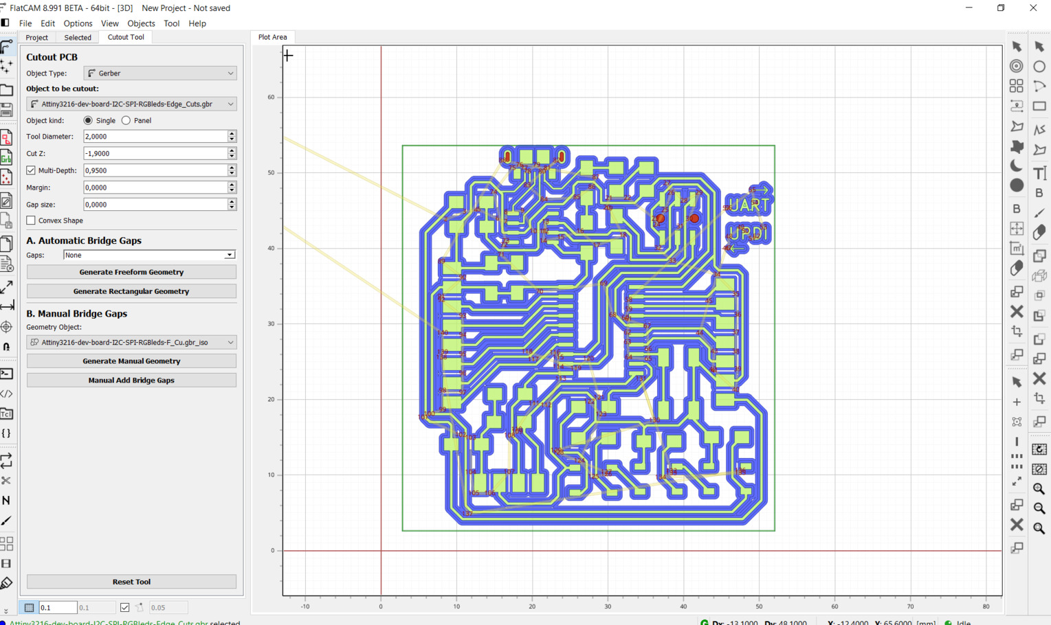
Steps to follow
- Export the F.Cu and Edge Cuts to grbr files
- If you have holes or slots to drill, export the excellon drill files
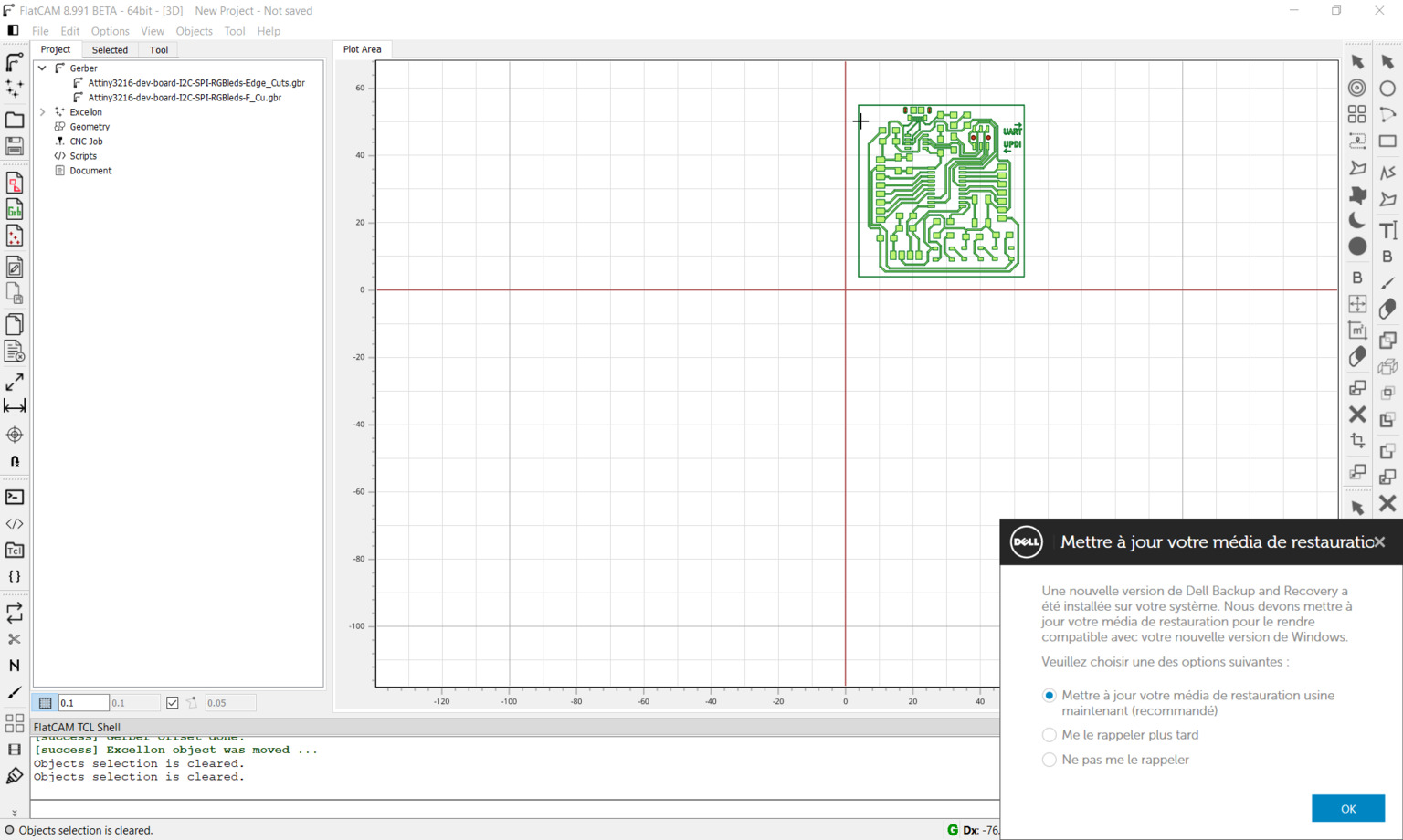
- Open the files in FlatCAM:
- Open FlatCAM
- Go in File > Open > Open Gerber
- If you have some drilling, go in File > Open
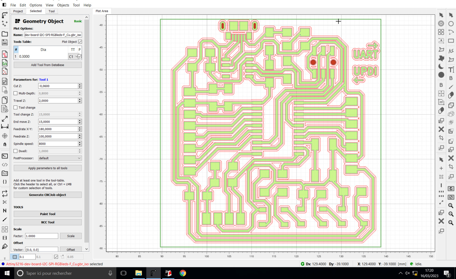
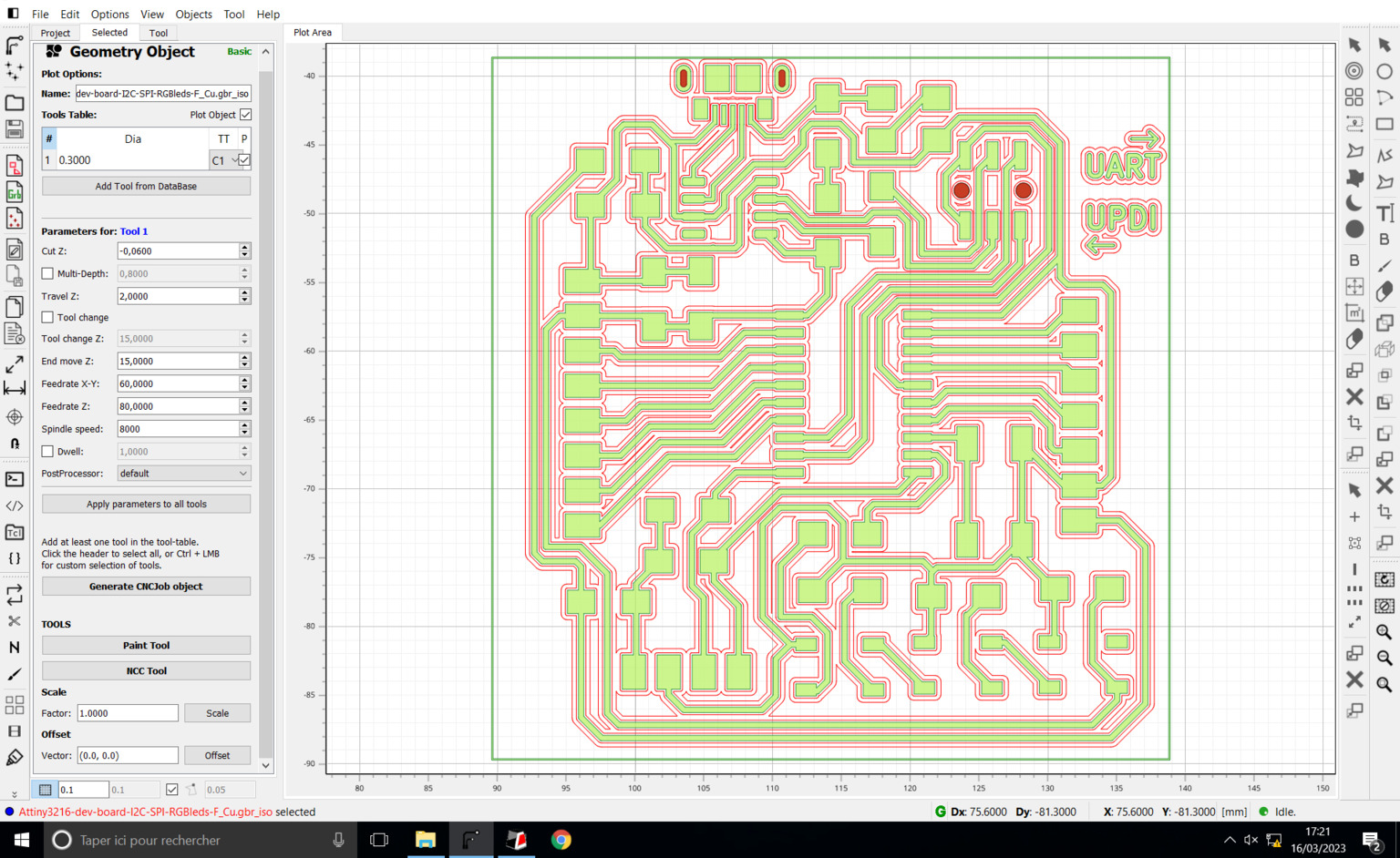
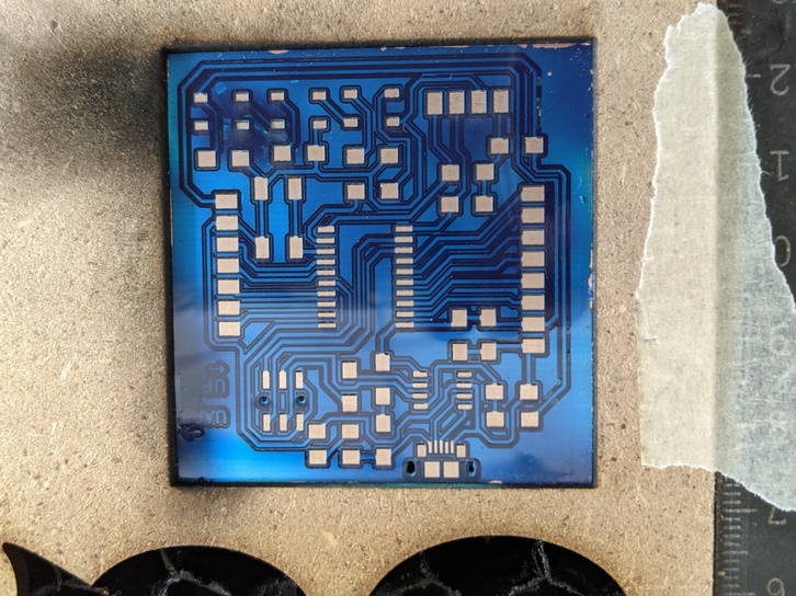
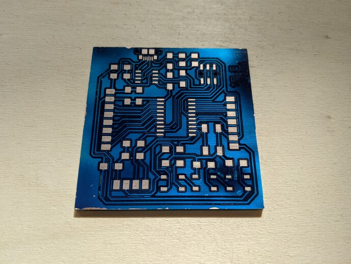
My settings and results
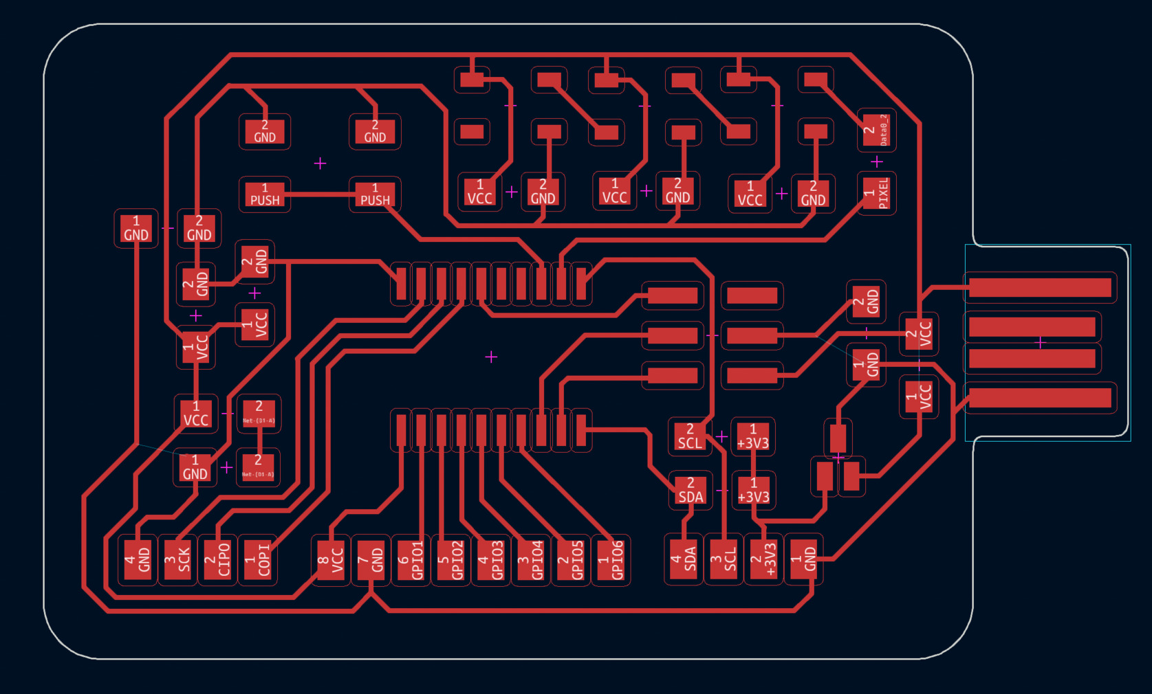
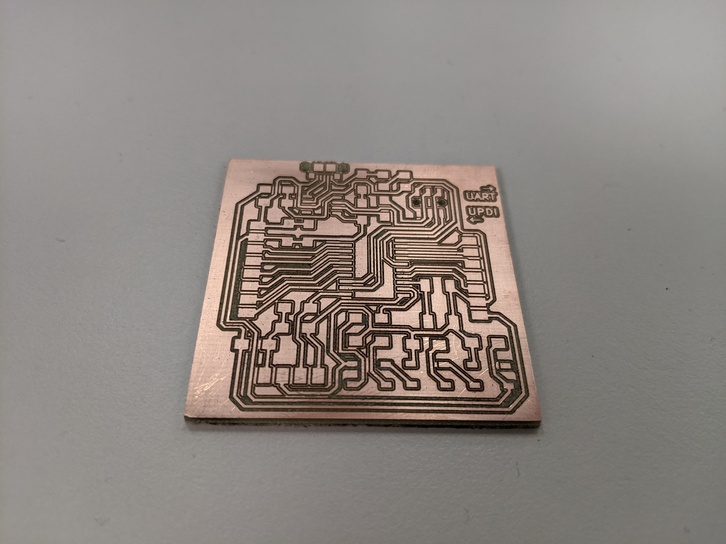
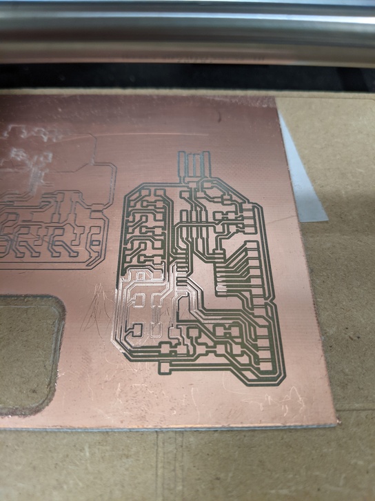
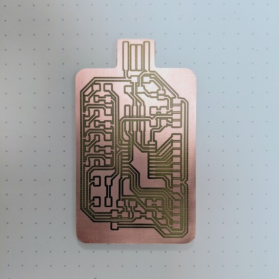
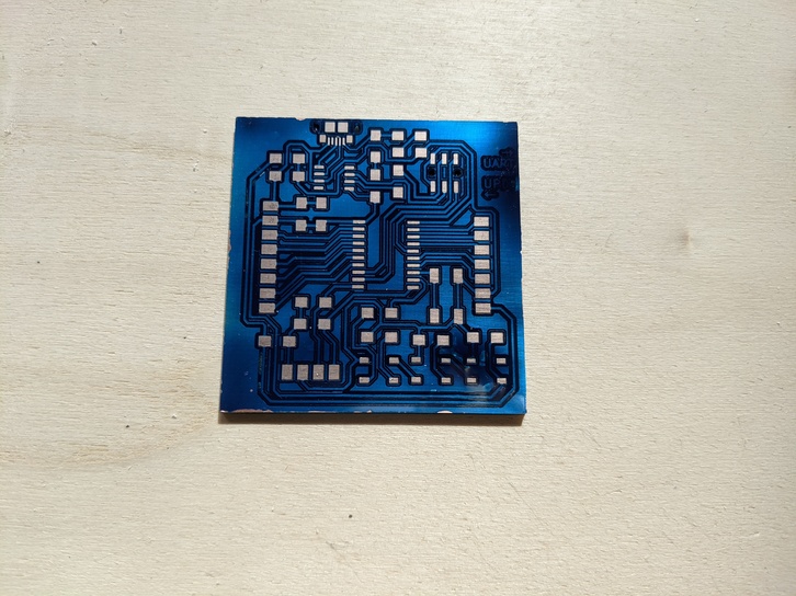
All the designs I machined were ATtiny 3216 development boards, with 3 RGB leds, a pushbutton, a USB port and lots of header pins to program it.
First circuit
- Design: it provides the following features
- CH340N component to program in UPDI through USB
- switch to go from FTDI to UPDI
- header pins for GPIOs, I2C, SPI
- micro USB port both to power and program / exchange serial information
- Settings:
- F.Cu tracks:
- 0.3mm diameter cylinder mill
- overlap 50%, 2 passes
- feedrate: 60 mm/min
- Slots and holes drills
- 0.4 cylinder mill for the drills
- cut Z: -1,8mm
- multidepth: 0.9mm
- Edge cut:
- 2mm cylinder mill for the edge cut
- margin: 0
- no gap size (it refers to the tabs you can add if your board has a chance to jump once cut, but not needed when you use double-sided tape)
- Cut Z: -1,9mm
- multidepth: 0.950mm
- F.Cu tracks:
I used the speed parameters in the table above.
-
Duration:
- F.Cu tracks: 1h05min... 2 times!
- drilling: 20s
- Cutting: 2min35s
-
Results:
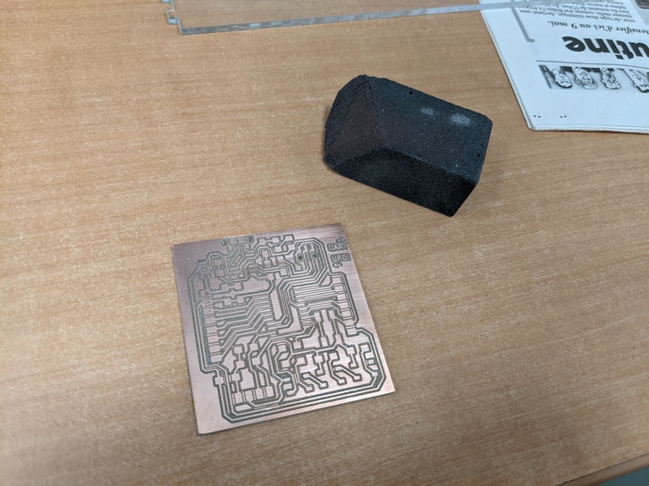
- It didn't suceed at the first try. The mill didn't go all the way through in an area of the circuit. It was probably because of the double-sided tape which wasn't evenly glued accross the board (some parts were higher than others.) I thus started the track milling a second time
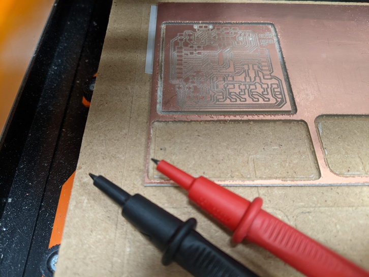
- The result is not very clean, the thin copper parts between some close tracks tend to deform, risking to shortcut some places of the circuit. I had to carefully observe it under the microscope and remove such thin threads with an exacto. I checked regularly with the multimeter that there were no shortcuts. I managed to have an okay result with no shortcuts
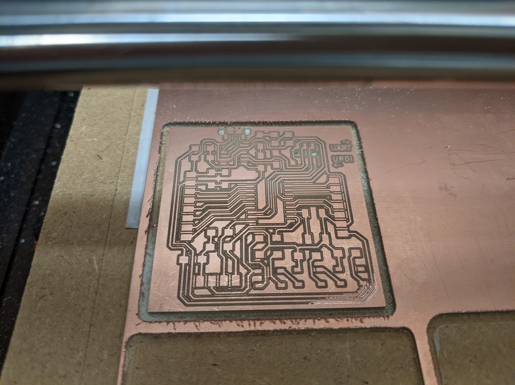
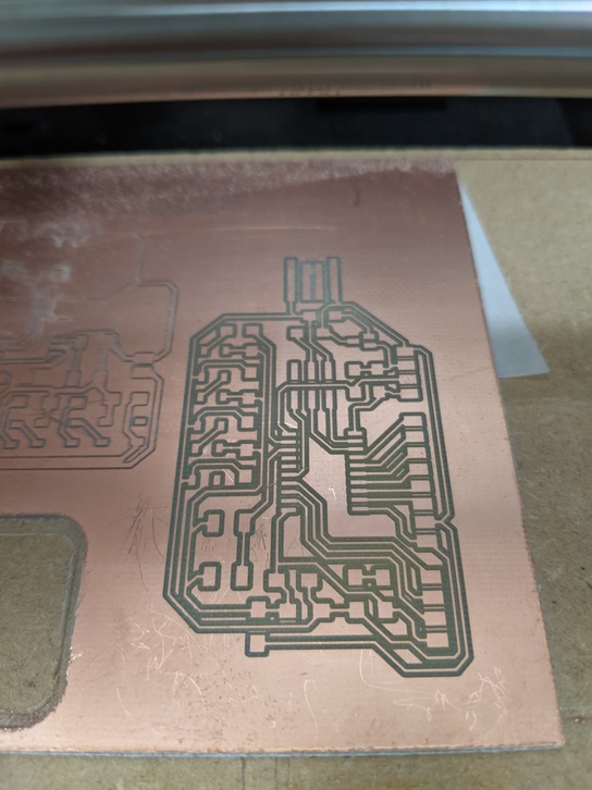
Second circuit
- Design: the same as in the first attempt except I rounded the edge
- Settings: the same as in the first attempt
- Duration: I stopped the milling midways
- Results: I broke the mill!
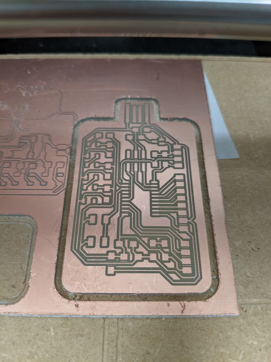
Third circuit
- Design: a simplified version of my development boad, which features:
- No more CH340N but a 6 pin vertical header to plug to a UPDI/FTDI programmer
- no more switch
- simplified header pins for GPIOs, I2C, SPI (SPI with only CLK, COPI and CIPO)
- a 3.3V regulator
- a plain USB A port
- Settings
- F.Cu tracks:
- 0.4mm diameter cylinder mill
- overlap 40%, passes 2
- No drills
- Cutout:
- 2mm diameter mill
- Cut Z: -1,9mm, multidepth 0,950mm
- No gaps
- F.Cu tracks:
- Duration
- 42min... 3 times!
Chemical etching
Principle
The principle of chemical etching of a PCB is the following:
- The tracks are exported in svg then arranged on a pdf (A4 size in France).
- The pdf is then printed on a transparent plastic sheet, to create a screen printing mask
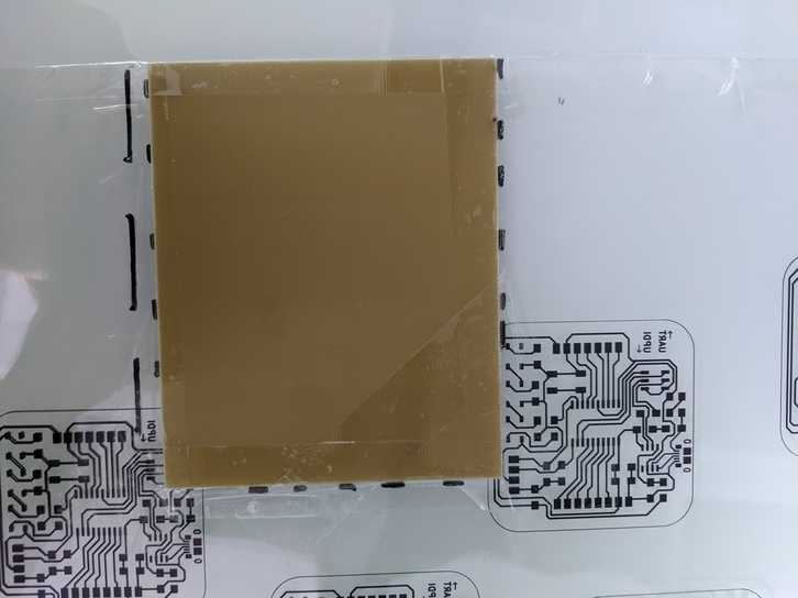
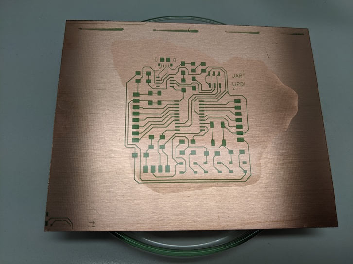
- The mask is taped on a special plate made of garolite, copper and a layer of UV-reactive resin
- This plate is then exposed to UV light to soften the resin on the plate except where the printed tracks block the UV light
- The plate is placed in an perchlorite iron bath which will react with the solid copper and remove it from the plate, except where the tracks are protected by the hard resin
- The hard resin is then removed with acetone
- It can optionnaly be tinned thanks to a tinning solution, which covers the copper tracks with tin to ease the hand soldering process.
Safety rules
Safety rules are very important in a chemistry lab. Here are some golden rules to follow any time you work in such a space.
- Wear closed shoes, tied hair, no jewels, closed pants in non-synthetic fabric going all the way down to your shoes.
- Wear a chemistry lab coat, closed
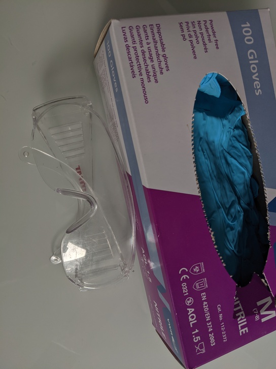
- Always read the safety pictogramms and detailed recommandations on the bottles / package of the chemical products you manipulate. Wear adequate individual equipments, such as throwable latex gloves and safety glasses. You also may need to work under ventilated hoods.
- If you use gloves, use them only once. Don't touch your cellphone with the gloves or anything that will go out of the lab afterwards. Don't touch your face
- Don't throw the waste in the sink: chemical waste should be sorted in separated jars depending on their pH.
- Gloves, tissue paper, plastic containers and all disposable material that may have touch chemical products should be thrown in a separate bin.
- Always wash carefully the glass reusable material you're using before leaving the lab (if possible, as soon as you finished using it)
- Wash your hands thoroughly after removing your gloves.
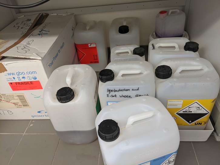
The plastic bins where chemical liquid waste are sorted according to their pH
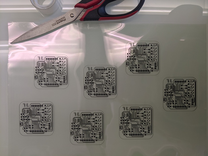
Create the mask
For this step you'll need:
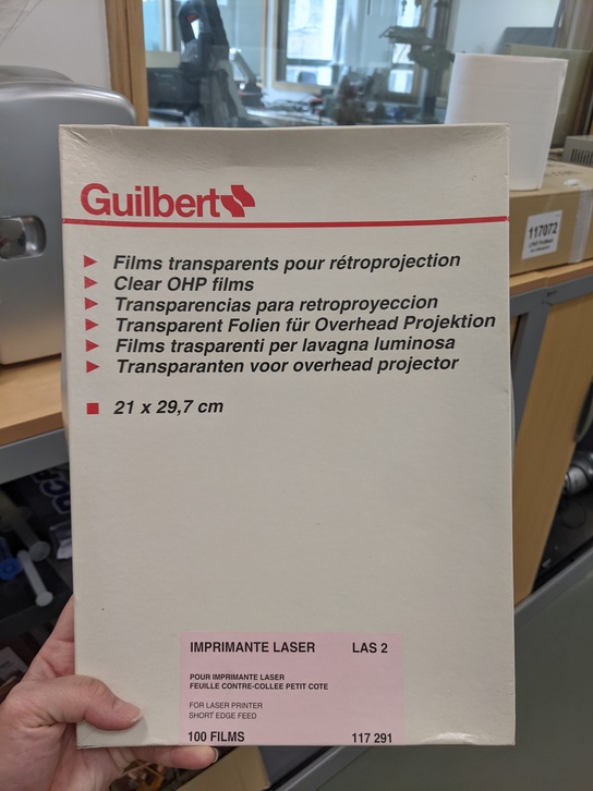
- transparent plastic sheets, as the ones we used to project writings with a retroprojector.
- tape
- cissors
-
a laser printing machine with black ink
-
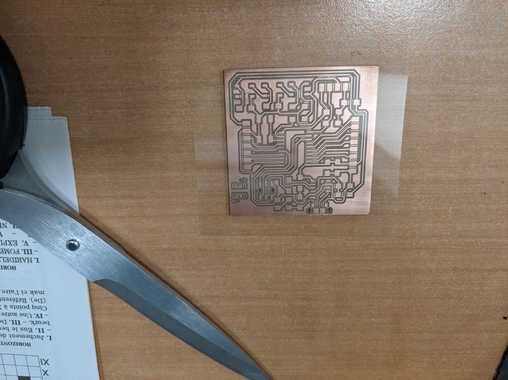
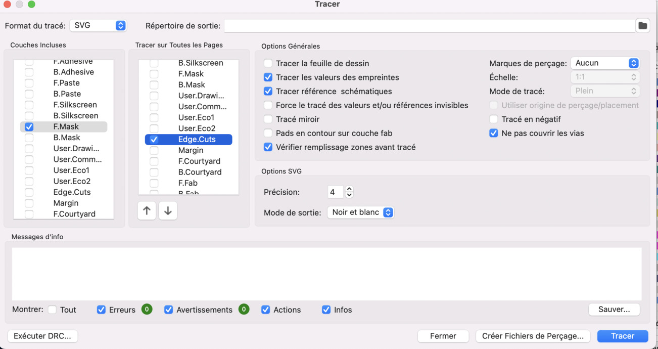
In KiCad, export the svg of the F.Cu and Edge cut: they must be on the same page, and you only want the area of the board. Don't select any technical layer
- Open it in Inkscape and resize your document to an A4 format. Group your circuit and copy it accross the A4 document. We only want to make one exemplary of the circuit so here we'll just place them rather randomly to avoid to encounter the plastic defaults several times.
- Print the pdf on a transparent plastic sheet, two times. Be careful not to adjust your document to the page whan you print it, but to keep the original size
- Examine the printed transparent sheets: you look for any default that could cross a track. Check that at least several circuit prints are very neat
- Place the two printed transparent sheets one on top of the other: you want them to be perfectly superposed.
- Tape the borders together to maintain the sheets correctly superposed.
- Choose the part of the mask you'll use by looking for imperfections.
UV Reaction
For this step you'll need:
- A special circuit making plate. It's made of:
- a thick layer of garolite
- a layer of copper
- a layer of UV reactive polymer resin
- dark tape to prevent the resi to cure
- your mask
- regular transparent tape
- a permanent marker pen
- a UV insoler
!! This step must be quickly followed by the next step !! You should prepare the next step before doing this one !!
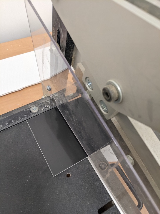
- If needed, cut the plate to obtain a size adequate to your circuit (count some margins, especially where you'll cut the plate with the massicuault)
- Indicate with a marker which side is the correct side to make your tracks (you don't want to trace them the opposite way!)
- Figure out where you will stick the plate to the mask: the wrong side of the mask is towards you and the plate lied onto it with the black tape towards the mask and the garolite part towards you.
- Mark the approximative place on the mask where you'll stick your plate to, using the marker.
- Turn down the lights in the room that you don't need to operate.
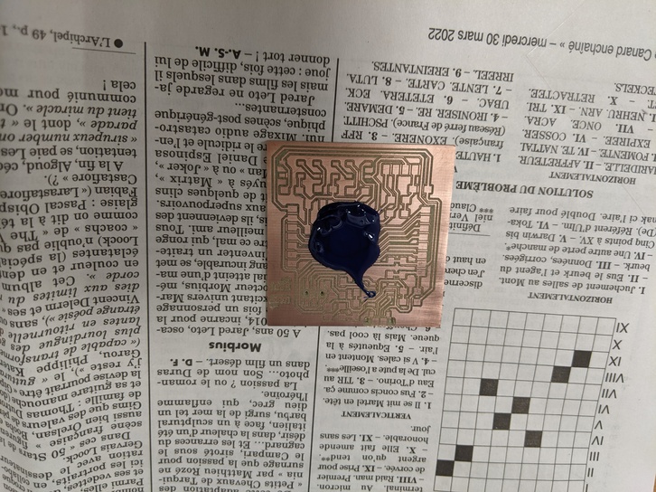
- With the black tape facing down (to the table), remove the tape. Nothing protects the reactive resin now so make sure to expose it to the minimum of light!
- Place the green reactive resin on the plastic mask, where you marked earlier a correct position.
- Tape the edges of the plate to the mask. You want it to be really flat and well maintained, but too much tape would be annoying
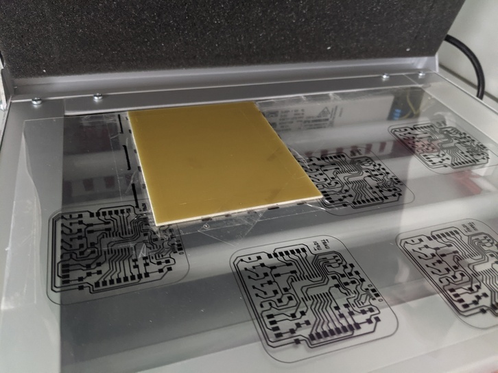
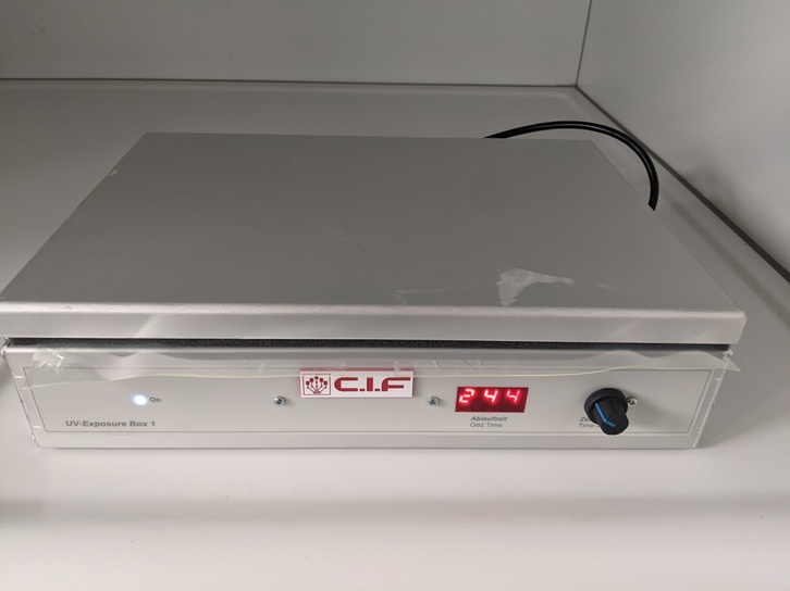
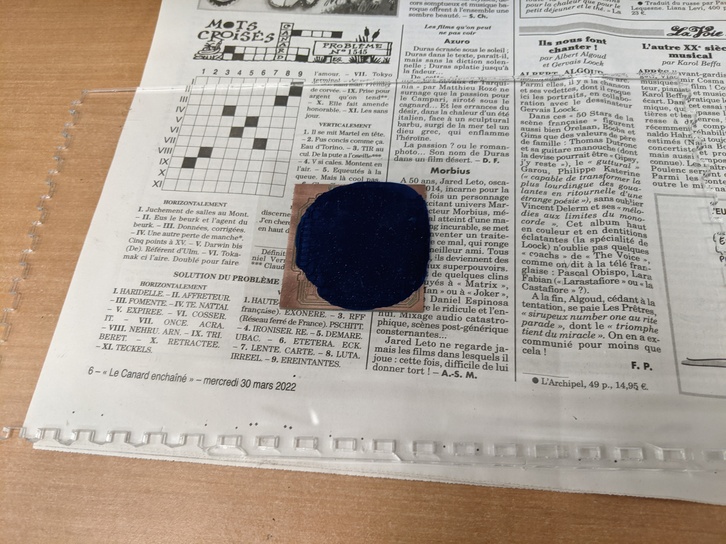
- When you're done, place the plate taped to the mask inside the UV insoler. If possible, seal the insoler box with the clips.
- Turn on the UV lamps of the insoler and immediately start the timer (our is integrated to the insoler). We placed it 3.00 minutes with the UV light on.
- Put your safety equipments on and check everything is ready for the next step
- Turn off the lamps and be ready to jump fastly to the next step
Cleaning the softened resin
For this step you'll need:
- Soude
- Distilled water
- 2 cristalizer: one to soak your plate, the other to rinse it
- a metal scoop to manipulate the plate while rinsing
- absorbing tissue
This must absolutely be done in safe conditions:
- Compatible clothing, shoes and hair tied
- Safety glasses
- Chemistry coat (closed)
- Throwable gloves (the right size for your hands)
Here's the process:
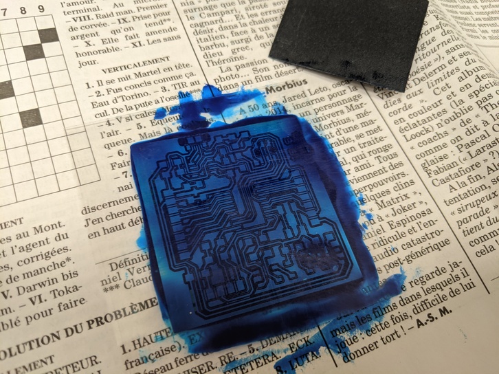
- Take the plate off the insoler and take off the transparent tape
- Put 1-2 cm height soude in the big cristalizer
- Place your plate in the liquid, without touching it and trying not to splash it either
- This will go fast!! Turn slowly the cristalizer with the solution and the plate. You'll see that the liquid turns darker and darker: the softened resin is going away from the plate.
- Continue doing these small moves until your circuit appears clearly and there are no more black traces. IMPORTANT : don't let your plate sit too long in the soude, because the solidified resin is the next to be removed, and you want to keep it to protect the copper!
- When the result satisfies you, clean your plate with distilled water above the other cristalizer.
Removing the copper
For this step you'll need:
- Iron perchloride (FeCl3)
- A plastic container
- Distilled water
- Moving platform machine
- tissue paper
- throwable gloves
The copper is removed in an iron perchloride (FeCl3) bath: the iron perchloride will react with the solid copper. This takes a while! We first only shook the plate in our Iron perchloride bath, then decided to place it on a moving platform machine of the lab to shake it continuously. It's also possible to heat the iron perchloride to accelerate the reaction. You know you're done when you can see all the copper has disappeared, except from the tracks. To sum up the steps are the following:
- Put some iron perchloride in the plastic container. It should be around 1-2 cm high to cover your plate, no need for more.
- Put the circuit plate in the plastic container
- Place the container on the moving platform
- Wait for the copper to be remover (approx 20-30 minutes)
- Stop the machine, remove the plate and rinse it with distilled water.
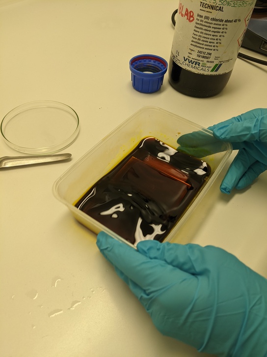
The plate is then washed with distilled water and wiped with a tissue paper.
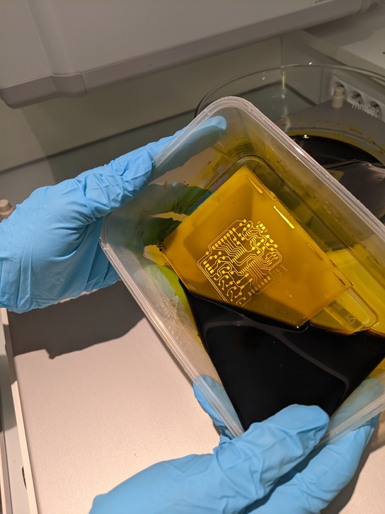
Removing the resin covering the tracks
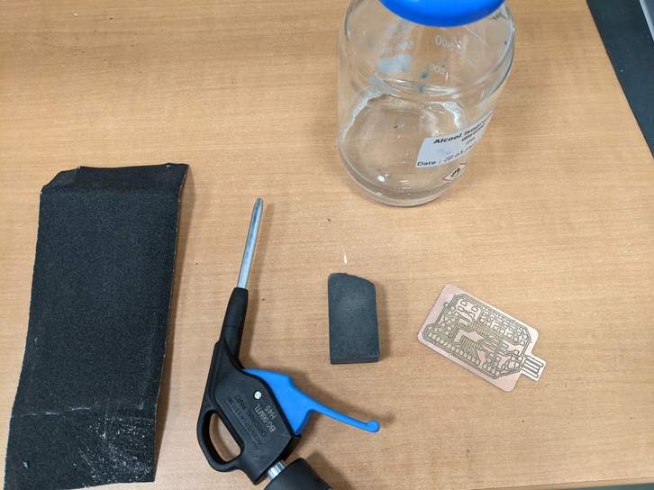
The copper tracks are stilled covered with resin: you can see on the previous picture that it's still greenish. To remove the resin we use acetone (in a ventilated area!) and tissue paper.
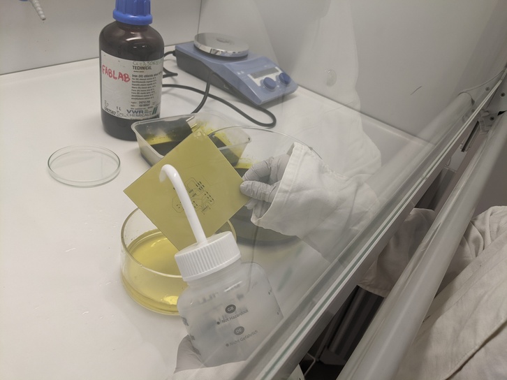
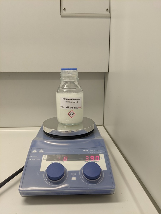
Tinning
Tinning (étamage) is optionnal but will help you solder more easily your components on your circuit. It consists in covering all the tracks with thin. To do so you need a tinning solution. Our is homemade with tin salt in HCl. For this step you'll need:
- tinning solution (containing tin salt and HCl)
- an agitating and heating machine
-
a container
-
Place the agitating magnet in the bottle of tinning solution and close it. Place the bottle on the heating and agitating machine.
- Turn it on to 200°C and wait until the salt dissolves: the solution should be almost clear.
- Place your tinning solution in the container
- Place carefully your copper circuit in the container, shake and take off the circuit when all the tracks are covered with tin (it goes really fast, only takes a few seconds)
Enjoy!
All that's left is to eventually drill holes where necessary, resize the board using a guillottine cutter and solder components. We hadn't recieve all the components yet so I didn't do the soldering on this board.
PCB varnishing
Principle
PCB varnishing is used to provide better isolation between the tracks, which eases the soldering process by avoiding short circuit. The process my colleage Manuel showed me is the following:
- Check for short circuits on your milled PCB and clean it carefully.
- Spread some UV-curing varnish over the whole surface of the PCB.
- Place it an UV insoler for a few minutes to cure the varnish.
- Remove the varnish cured on the components pads by etching it with a laser engraving machine.
- Clean it with acetone.
Material
You should work in a well ventilated place to prevent you from smelling too much acetone fumes. Ideally, work under a sorbonne.
- UV insoler machine
- Laser cutting machine
- Ideally: a sorbonne ventilating your work area
- A tube of UV reactive ink for varnishing PCB (to store away from the daylight)
- The plastic push seringe coming with the ink tube
- A transparent plastic sheet; some works better than other (they can either be peeled easily from the dried varnish or stay stuck to it). We use the ones shone in the pictures below.
- Le canard enchaîné (or any newspaper)
- A sturdy, thick and flat piece of plastic to first roughly spread the ink. We're using a piece of 3mm thick acrylic
- A piece of plastic to spread the ink more finely, it must be flexible enough but quite sturdy too. You can see the one we're using below. It looks like ~1mm thick PP.
- Scissors
- Abrasive eraser
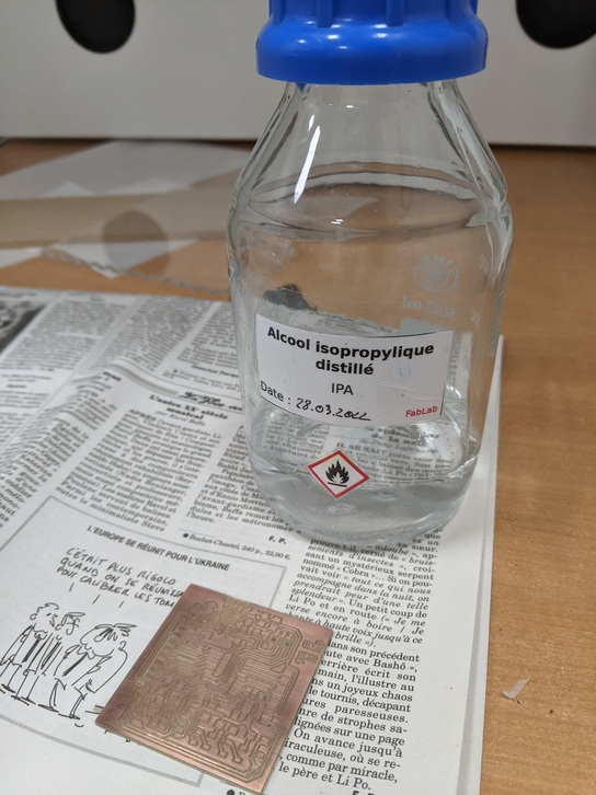
- Ispopropylic alcohol
- Acetone
- Compressed air (optionnal)
- 3mm MDF scrap to hold the PCB in place while etching with the laser cutting machine
- Absorbing tissue just in case :-)
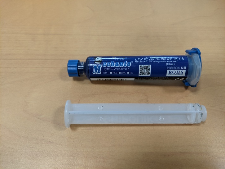
The ink we're using, a LVH-900 type by Mechanic
Varnishing with UV reactive ink
Best practices (recommanded by my colleague Manuel): * Start with a bigger edge cut in KiCad to avoid the excess varnish effect on the edge of your circuit * Do the drilling after the varnish, else you'll have varnish dropping in the holes
1- Clean well your PCB (abrasive eraser, compressed air, isopropylic alcohol)
2- Cut a piece of transparent sheet a bit larger than the PCB (but not too much)
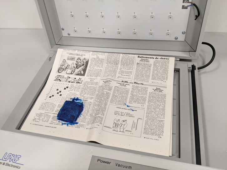
3- Place your PCB on the journal to protect the surface and put a little bit of ink on the middle of the PCB, using the plastic push syringe. Store the inkt tube back in its dark storage. On the pictures below you can see that I put a little too much ink.
4- Place your transparent sheet piece on top of the ink.
5- Spread the ink on the surface of the PCB: first place the thick plate (here the 3mm acrylic scrap) on top of the transparent sheet piece and gently press keeping the surface quite horizontal. That will spread roughly the ink on the board. Then to spread it more finely and homogeneously, use the flexible thin plastic 'spatula'. Start by removing the acrylic thick plate, but keep the transparent plastic sheet in place without moving it. It's okay if it slides a bit horizontally but not vertically, or you'll get some air bubbles. You want to have an homogeneous quantity of ink on the surface and to be able to see the tracks behind the ink.
6- Keeping the plastic transparent sheet on the PCB and the newspaper under, place the newspaper inside the UV insoler. Close the insoler and start it for 5 minutes. At the Fablab it's already set on 5 minutes, all you need is to turn it on by clicking on the black button.
7- After 5 minutes, take out the newspaper with the PCB on, and gently peel the transparent sheet. Your varnish is solidified!
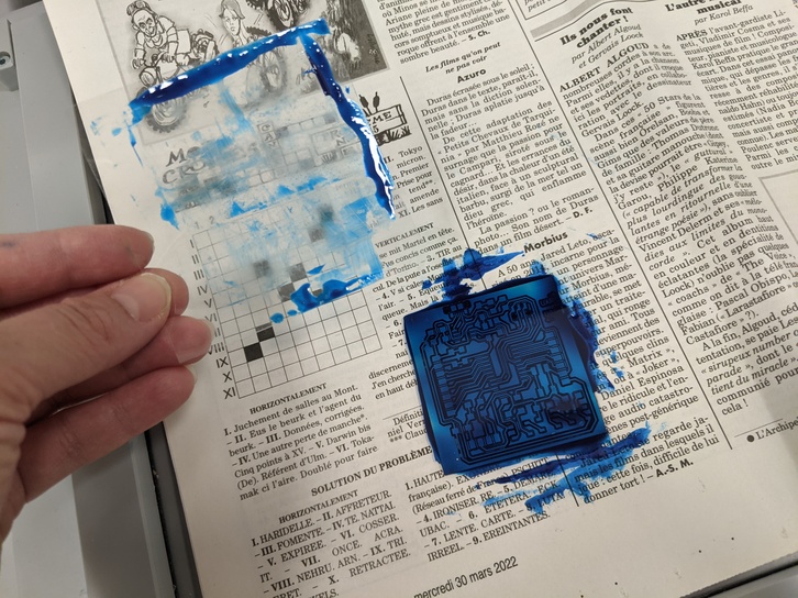
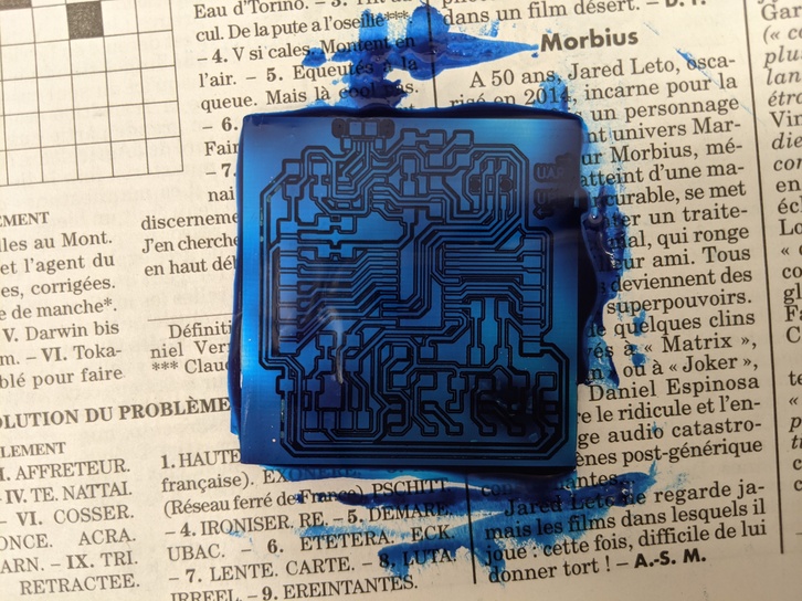
8- Always on the newspaper, remove the excess varnish on the edges with a cutter or an exacto, and wash off the soft varnish ink under the PCB with alcohol and a tissue paper. You're now ready for etching!
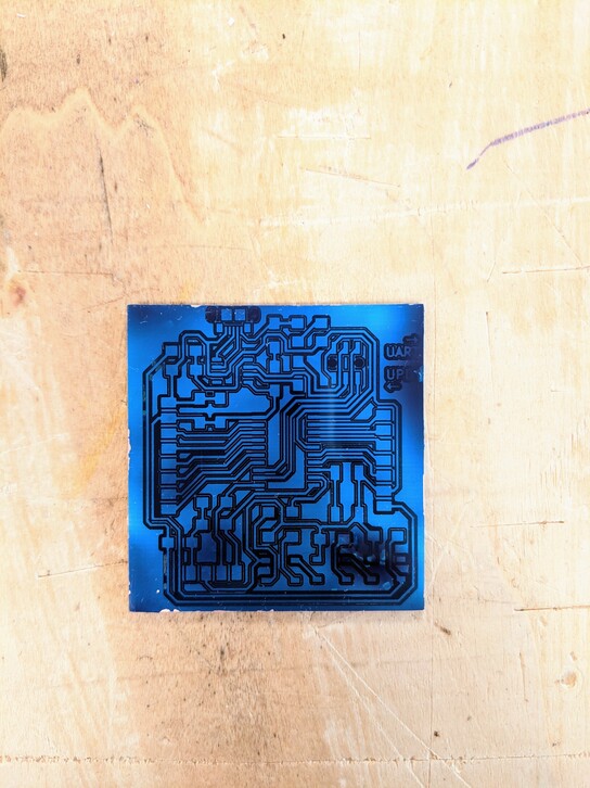
Etching the pads with the laser cutting machine
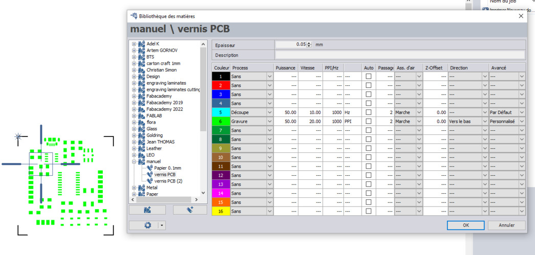
Export the pads in svg from KiCad plotting dialog.
Modify the svg to follow the color code recognized by your laser cutting machine. Here I've set the outline in red and the pads in green (make the shapes are all suitable for laser engraving, e.g. only closed shapes with no outlines, and not thick simple lines).
Open this design in you laser cutting software. I'll use the trotec Speedy 100 in our lab, because my colleague made all the settings tests on this one. Thus I open the design in Inkscape before sending it to Job Control thanks to the print dialog.
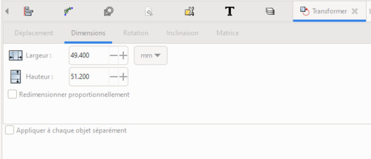
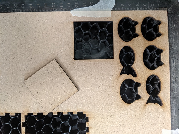
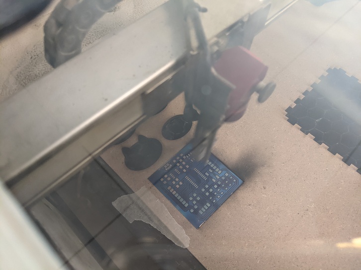
I started by cutting the outline in an MDF board: it should fit precisely the PCB. I've made several dimensions tests using the Transform > Dimensions window, until I obtained a tight fit.
Place the varnished PCB in the MDF's hole.
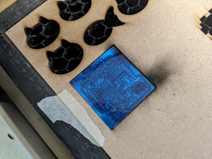
Disable the cutting and engrave the pads (in green on this file). I used the settings provided by my colleague (to be adapted according to your laser cutting machine in particular the laser power, and the lens):
- Power: 50%
- Speed: 20%
- Frequency: 1000 dpi
- Passes: 2
Enjoy!
Clean with acetone.
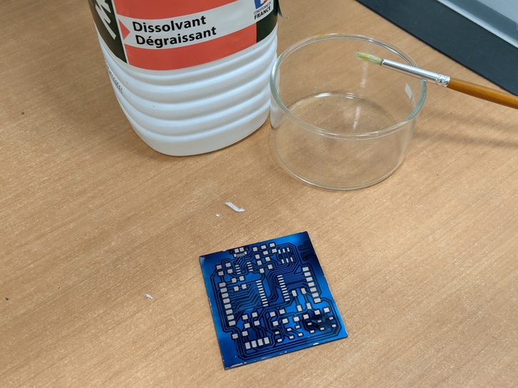
I faced an issue also faced by my colleague: it seems a very thin material layer still covers the pads, as the contact is not great from what I tested with a multimeter. Apparently he solved this situation a bunch of times using more acetone to clean thoroughly the thin deposit layer, but I didn't have the time to go further in this direction.
Soldering
I didn't solder my original circuit design because some components were still on their way. I soldered the components on my second design board. I didn't faced difficulties except for the neopixel RGB leds, which have their pads under the component (I should use solder paste next time).
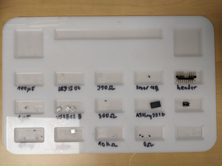
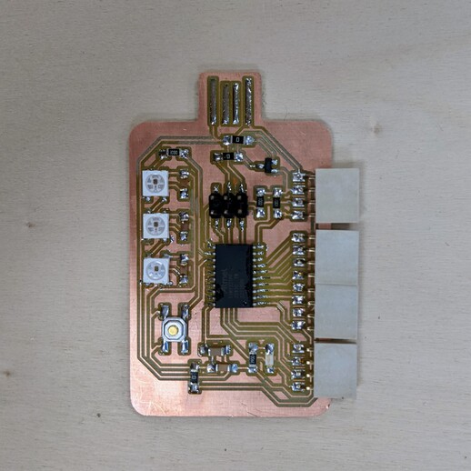
Testing
I managed to upload basic sketches through the updi programmer board: print a message in the serial monitor, turn on an LED. Unfortunately I have more trouble making the WS2812B neopixel leds to work, probably because of bad soldering (the pads are under the component, it's probably necessary to use solder paste).
[Edit]: I used this board for weeks during the Fabacademy and I am very happy with it! If you want to use a similar board, don't forget that you'll still need an external UPDI programmer, as the board provides an ATtiny3216.
Files
- Gerber files for the CH340N board designed during week 6
- KiCad and gerber files for the second board requiring an external programmer
- Screen mask in .svg for the chemical etching of the CH340N board
- Pads exported in svg to etch the varnish of the CH340N board with the laser cutting machine