Week 06 - Electronics Design
Goals
- design a development board to interact and communicate with an embedded microcontroller
- group project: use the test equipment in your lab to observe the operation of a microcontroller circuit board
Week's explorations and achievements
- I had almost no prior previous experience designing a circuit board
- I learned the various steps to design a circuit board using the software KiCad:
- define its specifications
- draw the eclectrical schematic circuit, eventually draw custom symbols or import them, for example from snapeda, and use the electric rules checker
- assign footprints to components and eventually modify or import footprints
- create a PCB's design and routing applying design constraints, and run the design rules checker
- I learned how to convert an easyEDA / LCSC part to a KiCAD part
- I designed my own development board, based on an ATtiny3216, using KiCad.
- We learned how to use multimeters, oscilloscopes and logic analyzers to test an electronic circuit (group assignment).
Steps to design a circuit
Here are big steps to design a circuit using the software KiCad.
A. Define your circuit's specifications
- Ask yourself if they are general design questions to take in account: maximum dimensions of the board, environmental constraints etc.
- Define the functionnalities of your board. You can list them in priority order.
- Are there some specifications necessary to achieve these functionaities? Such as bluetooth, a large SRAM, etc.
- Define the microcontrollers that will fit to your needs
- Start listing the components you will need
- List the references of these components - relying on the references you already have in stock when it's possible.
- For the most complex components, look for the datasheet to know the pinout, power specifications, etc. If your component must be used with resistors or capacitors, update your components list.
B. Draw your electrical schematic circuit
- In Kicad, create a new project and go in the schematic editor
- Add the components symbols using the symbol libraries. If you cannot find the one you're looking for in your symbol libraries you can:
- Import a new library
- Look for the symbol online, for example in snapeda
- Draw the symbol in the symbol editor, according to your components datasheet.
- Add power symbols
- Add wires to connect the components. You can use global labels to make a schematic easier to read.
- Add net labels (optionnal)
- Run the electrical rules checker
- Fix the problems detected by the rule checker
C. Assign footprints to the components
- In Kicad, run the footprint assignment tool
- For each component, look for the correct footprint using libraries and filters. You can check that it's the footprint you expect by right-clicking on it then View selected footprint
- Double click the footprint to assign it
- If you can't find the footprint you're looking for, you can look for it online, for example in snapeda. Download it, then go in the footprint editor, select the library you want to import the footprint in, then go in File > Import
- Some components have generic packages, look which one you should choose by browsing their datasheet.
- You may also want to modify some footprints, for example if you believe they will be hard to solder. Use the footprint editor to redraw them.
- Apply changes, save and close the footprint assignment tool.
D. Create your PCB's design and routing
- In Kicad, open the PCB editor and update the PCB according to the schematic. All footprints appear, start by clicking anywhere
- Ask yourself some design questions:
- Are there shapes and dimensions to respect for the global board edge cut?
- Are there some components that must be oriented or placed in a certain way? For example a USB port, and power input, head pins, etc.
- Are there some components which need to be physically close one to another? For example capacitors near the microcontroller
- Will you make a double-sided PCB or not?
- Place the footprints approximatively, according to the previous points.
- Set your design rules. Go in File > Board setup > Design rules
- Specify the design constraints according to the process you'll use to machine the board. For example, if you mill it in your lab, take in account the size of your milling tool. If you send your design to a professionnal PCB making company, use their specifications
- Add a predefined width for your tracks, again according to your tools or the PCB fabricant.
- Save your changes and go back to the PCB editor
- In the PCB editor, mask the layers you don't want to see
- Select the F.Cu layer. Choose the correct track width then use the track routes tool to connect the pads.
- If necessary rotate and move the footprints
- You may want to change some electric wirings in your schematic, for example change the microcontroller pin you wired a component to, because it will be more convenient for the routing. In this case go back to the schematic editor and don't forget to update PCB with changes made to the schematic when you'll go back to the PCB editor
- Select the Edge cut layer and trace the contour of your board
- You'll have other steps if you're creating a double-sided PCB, such as routing the B.Cu and adding vias, but I only learned the single-sided PCB design 8-)
- Run the Design Rules Checker
- Fix the problems
What's next?
We'll export the files to mill the circuit during the Electronic Production week. Stay tuned!
Notes: Convert an easyEDA / LCSC part to a KiCAD part
I faced the situation when I wanted to import a switch that I couldn't find in KiCad, neither in the symbols nor in footprints etc.
This is the component, a K3-2380S-E1 from Korean Hroparts Elec that you can find here.
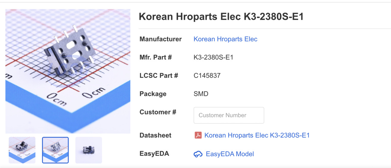
The website allows us to see and open the part in EasyEDA (by clicking on free trial). It also provides the LCSC part number.
It then allows the EasyEDA editor, allowing us to export the component in EasyEDA format. ![image screen easyeda export]() -->My instructor advised me to use the following library that allowed me to convert the EasyEDA/LCSC part to be able to use it in Kicad: easyeda2kicad.py.
easyeda2kicad.py is a Python script that converts any electronic components from EasyEDA or LCSC to a Kicad library including 3D model in color. This tool will speed up your PCB design workflow especially when using JLCPCB SMT assembly services. It supports library formats for both Kicad v6.x and Kicad v5.x.
Here's how to use the easyeda2kicad library.
- If it's the first time, install it:
- download the
.zipfrom the [github page]((https://github.com/uPesy/easyeda2kicad.py) - unzip in your Kicad folder
- open your terminal then
pip install easyeda2kicad
- download the
- Copy the LCSC number part. In my case it was
C145837 - In your terminal, go in you Kicad folder
- Run one of the following command, replacing the id after
lcscwith your LCSC number part
# For symbol + footprint + 3d model (with --full argument)
easyeda2kicad --full --lcsc_id=C2040
# For symbol + footprint + 3d model
easyeda2kicad --symbol --footprint --3d --lcsc_id=C2040
# For symbol + footprint
easyeda2kicad --symbol --footprint --lcsc_id=C2040
# For symbol only
easyeda2kicad --symbol --lcsc_id=C2040
# For footprint only
easyeda2kicad --footprint --lcsc_id=C2040
# For 3d model only
easyeda2kicad --3d --lcsc_id=C2040
# For symbol in Kicad v5.x legacy format
easyeda2kicad --symbol --lcsc_id=C2040 --v5
I ran this command: easyeda2kicad --full --lcsc_id=C145837
- All converted parts will be created and placed in subfolders in a easyeda2kicad folder.
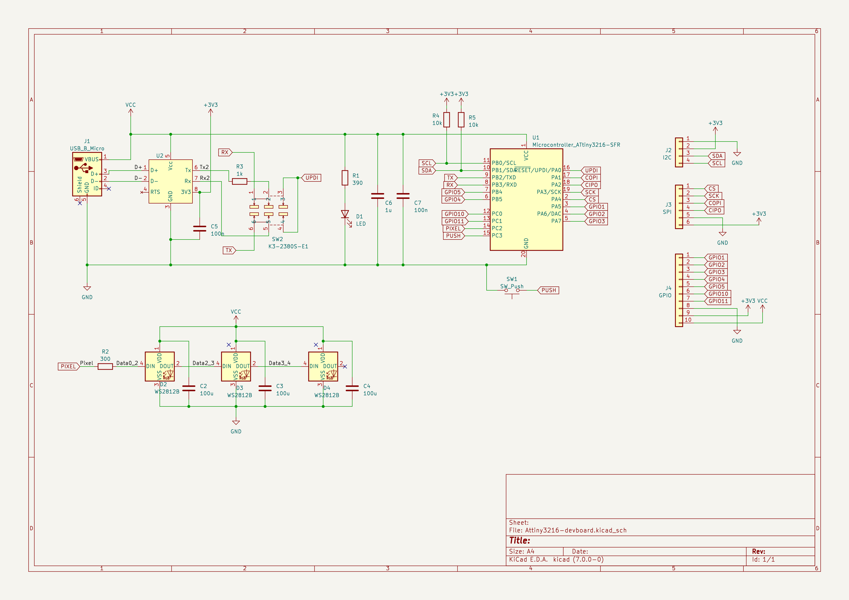
My circuit
I'll document how I designed my circuit following the steps listed above.
A. Defining my circuit's specifications
- I don't have any general design constraints. I don't need a particularly small circuit and will take margin if necessary, since it's my first board and it has a pedagogical purpose.
-
I want my board to have the following functionnalities:
- being a development board for a common microcontroller, which means I need available GPIO to wire some external components and also a way to upload some code
- provides a few RGB leds
- provides some basic built-in components (led indicating that it is powered, pushbutton)
- I know I want to try my RFID reader with it so an SPI header would be nice (as I used it with SPI in the Embedded Programming assignment)
- Also an I2C header would be convenient for a lot of sensors and components.
-
About the specifications:
- I don't need bluetooth or wifi.
- I may have some small real time calculous for the built in RGB LEDS and other neopixel strips I might connect it to.
- It would be better to have quite a lot of PINs as I want it to be polyvalent for various prototyping projects.
- Providing I2C and SPI communication
- a board simple to program using the Arduino interface and easy to use with its usual libraries would be great
-
From the previous specs I decided to use an ATtiny3216, which provides numerous pins, a decent flash memory, SPI and I2C interface, and is nicely compatible with Arduino libraries. In the datasheet we can thus read the following informations:
- Memories: 32 KB In-system self-programmable Flash memory, 256 bytes EEPROM, 2 KB SRAM
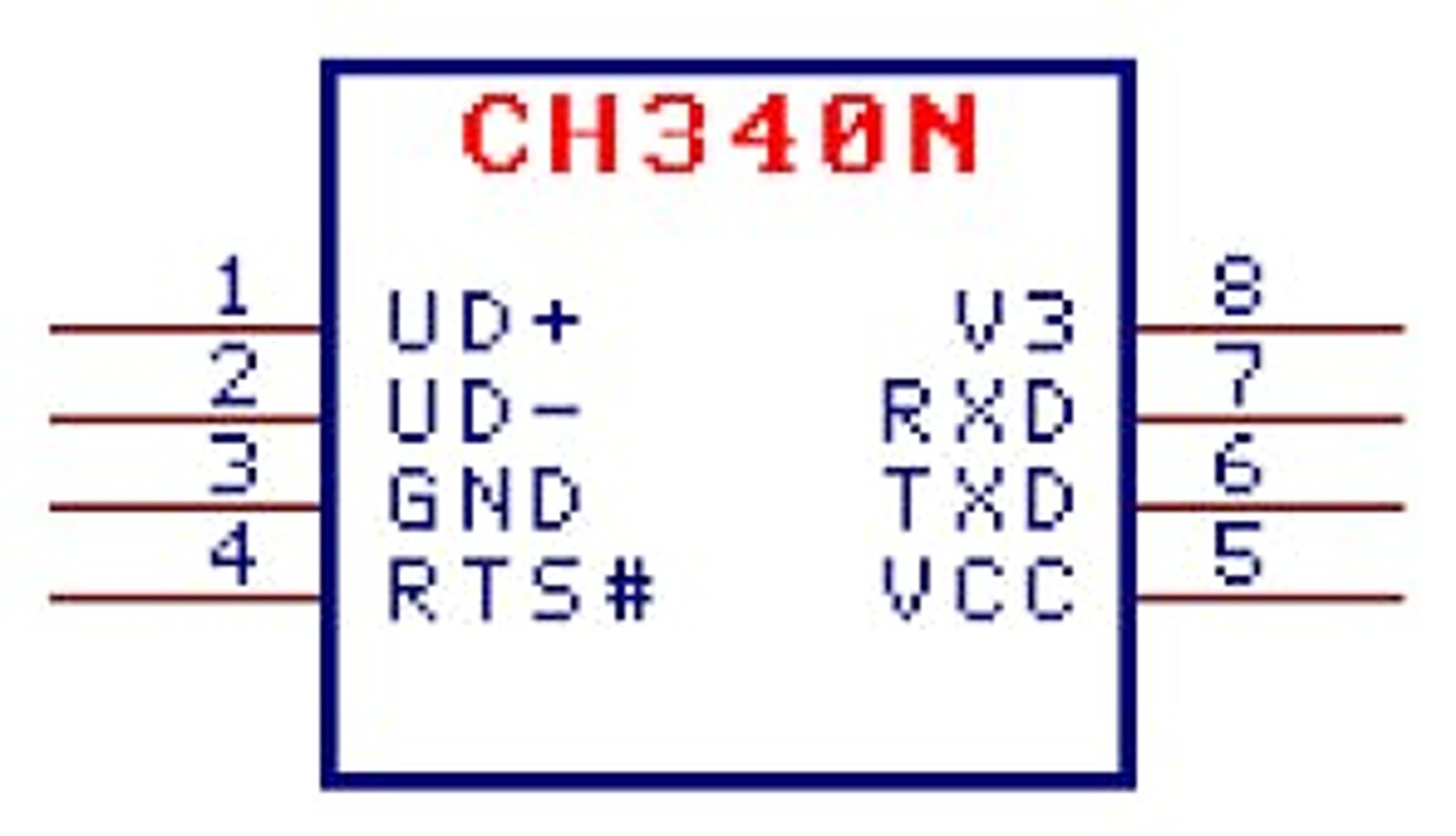
- Interface: UART, SPI, I2C Also, my instructor told me about a component which can convert USB signals in UPDI (and FTDI). This will be very convenient to program my ATtiny, because I won't need the physical UPDI programmer board anymore if this work (see Embedded Programming).
- I started writing a list of generic components I needed. I'll only include here the more detailed list, in the point below.
- Here is the list of components:
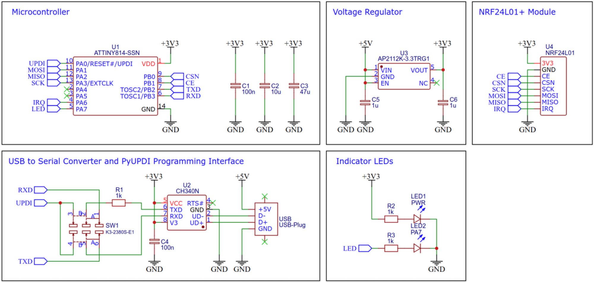
Components name Description, use Value / Specs Package informations Datasheet or vendor link ATtiny3216 Microcontroller SOIC8 datasheet 2 capacitors Filter the signal for the microcontroller 1uF and 100nF 1206 CH340N Convert the USB signals to UPDI/FTDI SOP8 datasheet 1 capacitor Filters the signal for the CH340N 100nF 1206 K3-2380S-E1 6 legs switch to go alternate between UPDI and FTDI conversion vendor 1 resistor Placed between Rx and Tx for UPDI signal 1kOhm 1206 USB3076-30-A microUSB port to exchange information with the computer and to power the circuit (5V) type B 1 led simple led to indicate if the board is powered yellow 1206 1 resistor to protect the simple led 390 Ohms 1206 1 pushbutton to interact Omron B3SN 3 WS2812B RGB leds datasheet 3 capacitors to filter signals for each RGB leds 100uF 1206 1 resistor on the data line of the WS2812B 300 Ohms 1206 10 pins header horizontal for the GPIOs, GND and Vcc 1x10 2.54mm 6 pins header horizontal for the SPI communication 1x06 2.54mm 4 pins header horizontal for the I2C communication 1x04 2.54mm 2 resistors pull-up resistors for SDA and SCL 10kOhms 1206 -
I linked the datasheets in the table above. Here are some pinouts though:
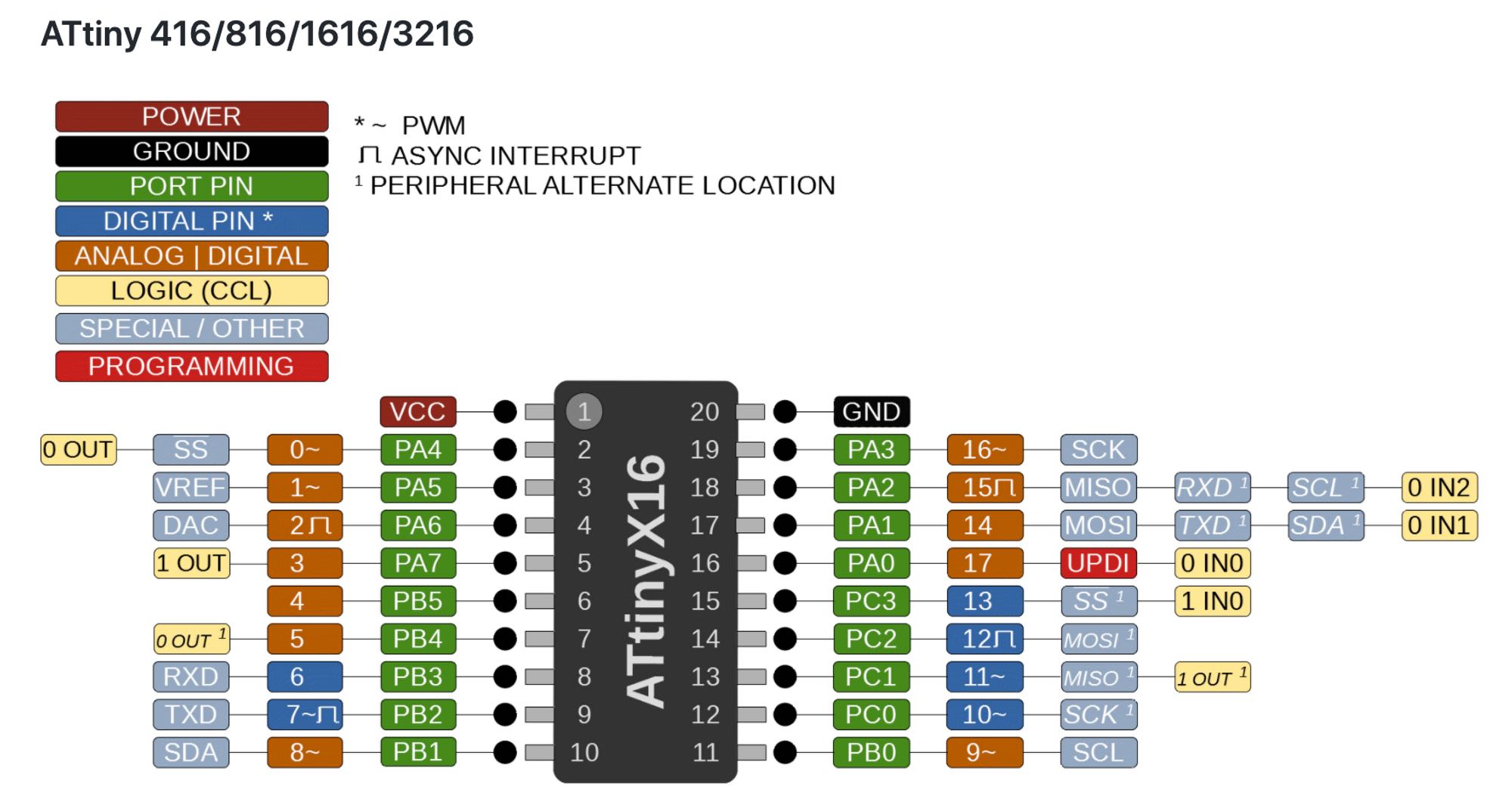
The pinout of the ATtiny will be useful to decide which pin I'll use for the built-in components, GPIOs and to wire properly the communication pins.
I also used the following schematic to wire properly the switch that will allow me to go from UPDI to FTDI protocol.
(source)
B. Drawing my schematic
-
I created a new project in KiCad and opened the schematic editor. Most of the symbols were easy to find.
- I used the ATtiny3216 in the fab library
- I used pin headers from the library Connector_Generic
- I used an USB port from the library Connector (that is the USB_B_Micro)
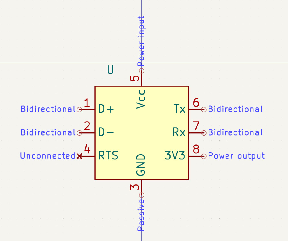
- I created a new symbol for the CH340N. I used the datasheet to know how to label the pins and their purpose. I wasn't sure about the pins electrical type.
- I used the easyeda2kicad.py python script to create a KiCad symbol for the switch from its LCSC number (see section Convert an easyEDA / LCSC part to a KiCAD part). I then uploaded the
.symfile in the symbol editor. - At first I made a mistake using WS2812 symbols instead of the WS2812B symbol. They don't have the same number of pins!
- I used three types of power symbols:
- GND
- VCC
- +3V3
- I added global labels and wired my components.
- I added net labels. At first I also labelled the global labels wires but my instructor told me that was unnecessary.
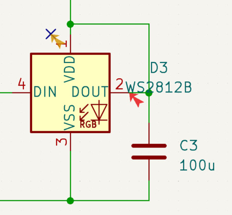
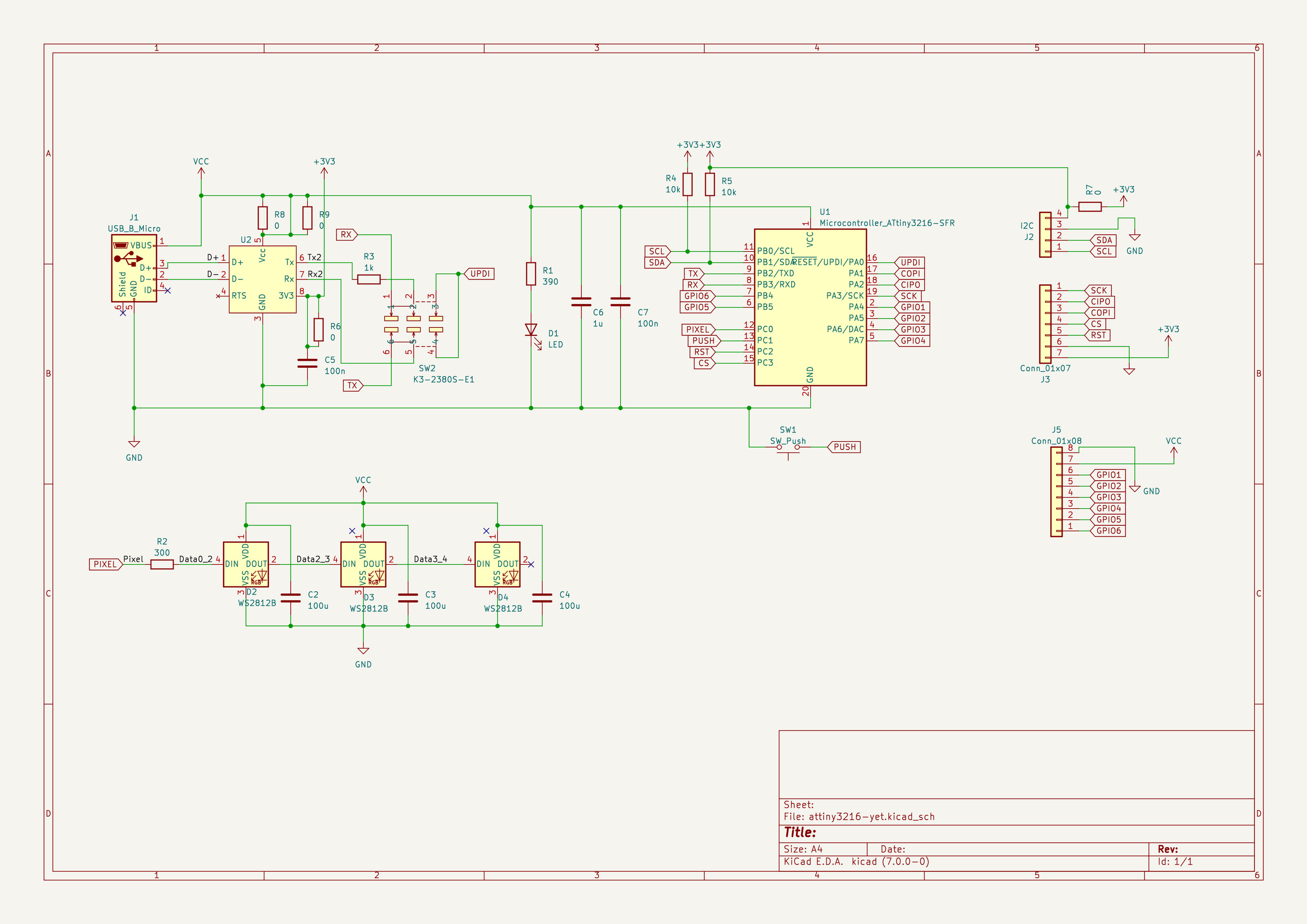
- I ran the electrical rules checker. I had some errors:
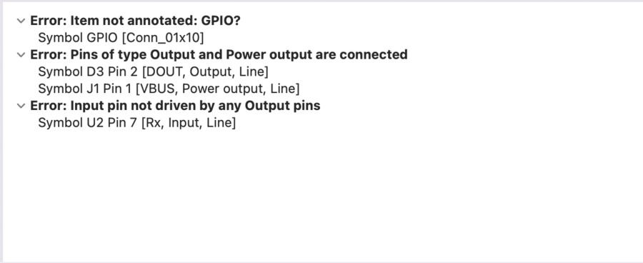
- Here's one mistake I detected and fixed:
It also indicated me I had errors with the electrical types of the CH340N's pins. I changed the 3V3 output pin to a power output pin, and the Rx and Tx for Bidirectionnal.
Finally here is my schematic:
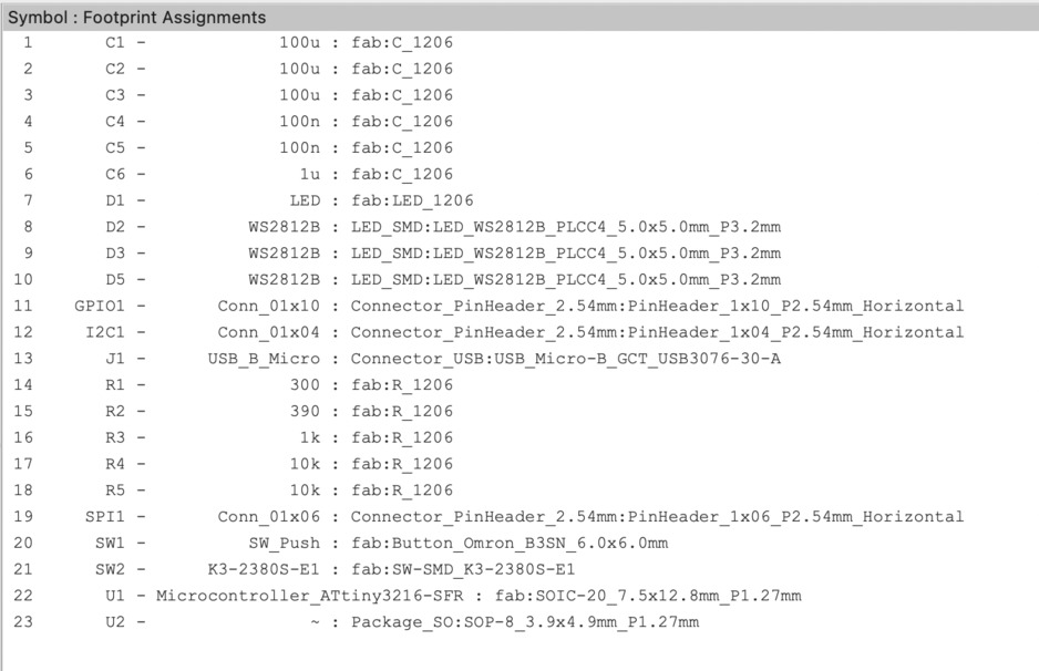
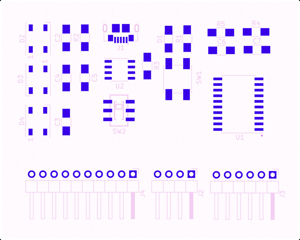
C. Assigning the footprints of my components
I didn't encounter any particular issue assigning the footprints. Here are some very small remarks:
- For the switch I uploaded the
_modfile generated thanks to the easyeda2kicad.py python script - I knew which generic package to use for the CH340N thanks to the datasheet.
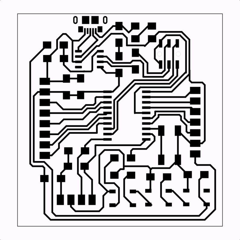
Finally here is a screenshot wich summarize all the footprints I chose:
D. Routing the tracks
- I opened the KiCad PCB editor then updated the PCB according to the schematic. All the components footprints appeared.
-
I answered to the following design questions:
-
Are there shapes and dimensions to respect for the global board edge cut? No, apart from the milling machines maximum dimensions.
-
Are there some components that must be oriented or placed in a certain way? For example a USB port, and power input, head pins, etc. No particular restrictions, I changed my mind several times which doesn't have any wtrong consequence.
-
Are there some components which need to be physically close one to another? For example capacitors near the microcontroller Yes, I have to place the corresponding capacitors near the microcontrollers, the CH340N and the WS2812B leds.
-
Will you make a double-sided PCB or not? Not, I'll do a single-sided PCB
-
-
I placed the footprints approximatively.
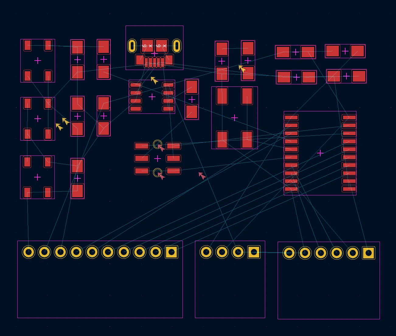
I also exported them in
.svgto be able to draw fancier routes another time. -
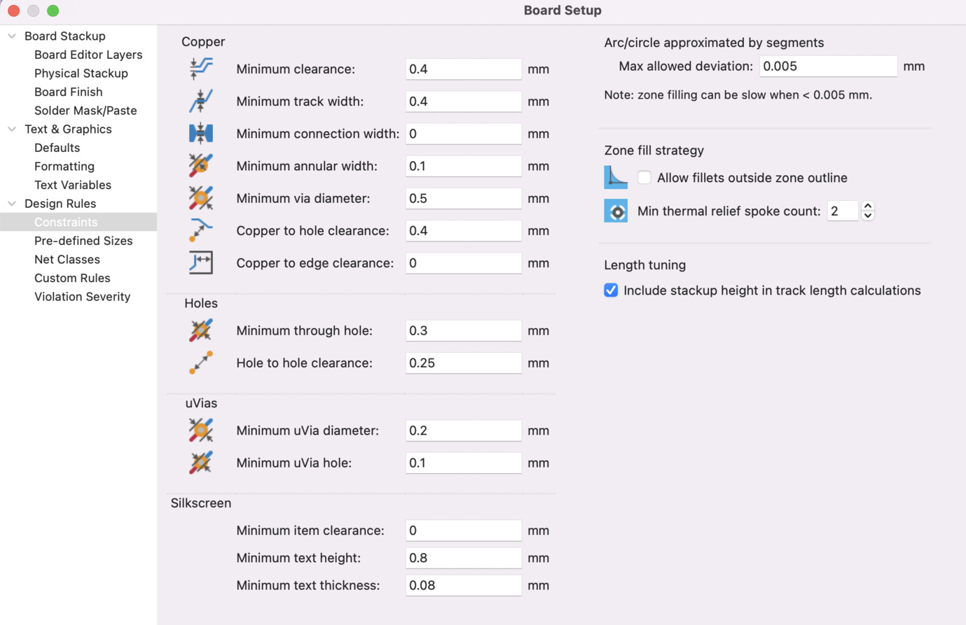
Design rules:
-
Design constraints: I set the minimum clearance to 0.4mm and minimum track width to 0.4mm, because I will use a 0.4 diameter milling tool. I had to change the design constraints for 0.2mm clearance at one moment, for the USB port which has very close prints. I am not sure if I shouldn't change the track width here rather than the clearance between the tracks.
-
Predefined width of tracks: I also chose 0.4mm for the track width.
-
-
I traced tracks with the predefined 0.4mm width on the F.Cu layer.
-
I had to rotate and move my components a lot te avoid tracks crossing.
-
I also had to change some pins in my electrical schematic.
- I changed the PIXEL and PUSH wiring for other pins of the ATtiny placed on the other side
- I and changed the order of the pins of the pins header
- I used another pin for CS (for the SPI) since its said to be reconfigurable, and also added a RST pin (also reconfigurable)
- I deleted the 3.3V output of the bigger pin headers since I already have two of them on the I2C and SPI headers.
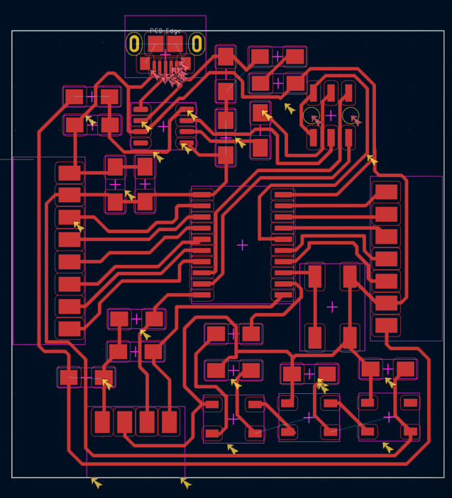
Finally here is my schematic after some modifications I did during the routing step. You can see some 0 resistors I'll talk about later.
-
For the outline I just traced a rectangle on the edge cuts layer. That's when I realized (too late!) that my design had a big problem around the USB port: some tracks were drawn outside of the PCB's border. I was good for some intense re-routing.
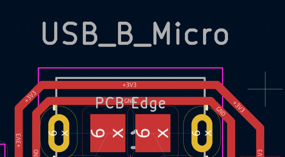
That was really an intense experience! Finally the outline measures about 50mm*50mm
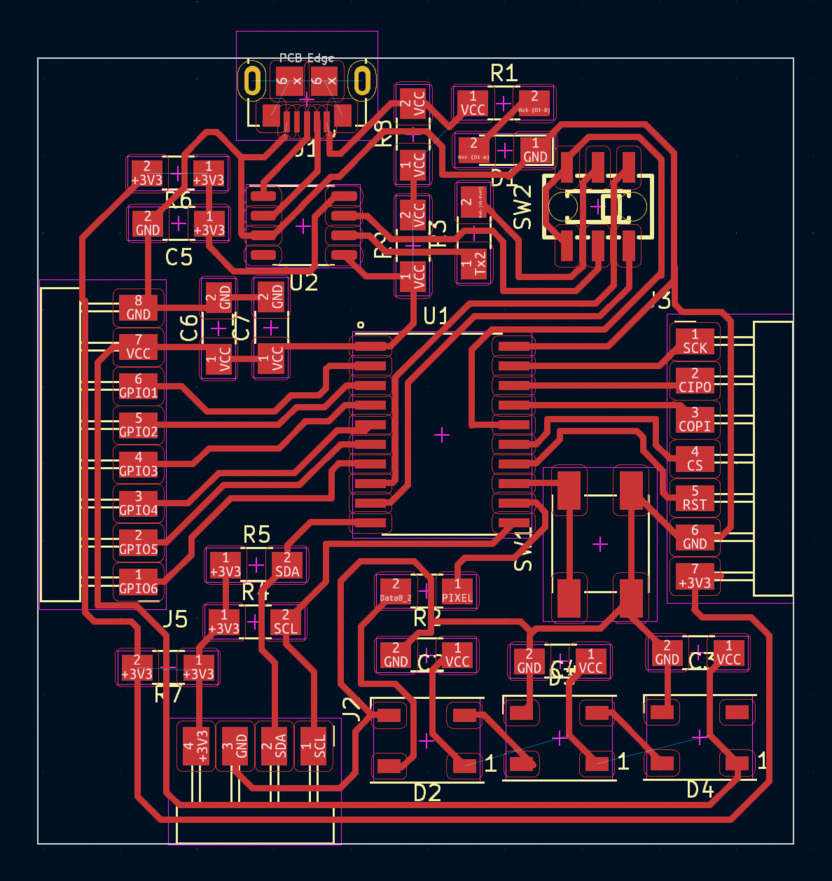
At the end I struggled with the three power lines
GND,3.3VandVCC. I managed to route everything by adding 4 zero ohms resistors. They will act as 'bridges' and allow me to cross other tracks.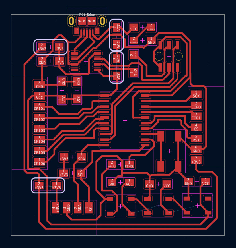
A hero shot.
-
No vias or B.Cu since I am doing a single sided PCB.
-
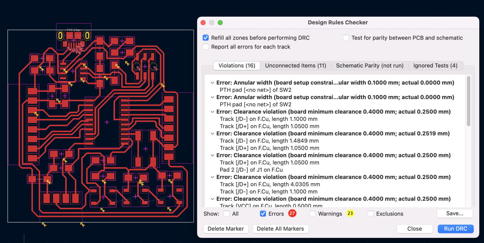
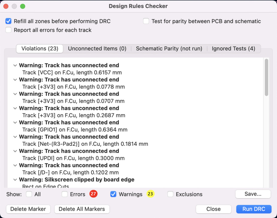
When I ran the DRC I had a lot of errors and warnings, but nothing really troubling I think.
- The clearance violations concerned the USB port, which I was aware of since I myself set different clearance rules here to be able to route my tracks to its pads.
- I also had annular width constraints problems on my switch. Not sure what I should do about it.
- I had a lot of warnings about silkscreen overlapping but this has no consequences since I am not using a silkscreen
- I had some warnings about not connected ends but I think at first view that it is normal.
 (
(
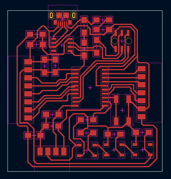
I exported the F.Cu in svg to enjoy my successfull routing (at least I hope so).
Group assignment
This week's group assignment was about measuring equipments to test your electric circuit.
Files
- KiCad project containing the schematic and PCB design