6. Electronics Design
This week I worked on designing a PCB board using two different schematic-PCB designing softwares while also planning out my design using a modeling simulation software. I also soldered a SEEED Xiao RP2040 board as a sort of programmer/breakout board type of deal.
Group Work
For this week my group and I tested the SEED Xiao Rp2040 chip using an oscilloscope and a multimeter. You can see my work on the maximum voltage test with an oscilloscope along with my group member’s Dariyah Strachan, Dylan Ferro, Stuart Christhilf, and David Tian work on the Charlotte Latin Fab Lab site for student group B.
RP 2040 Breakout Board
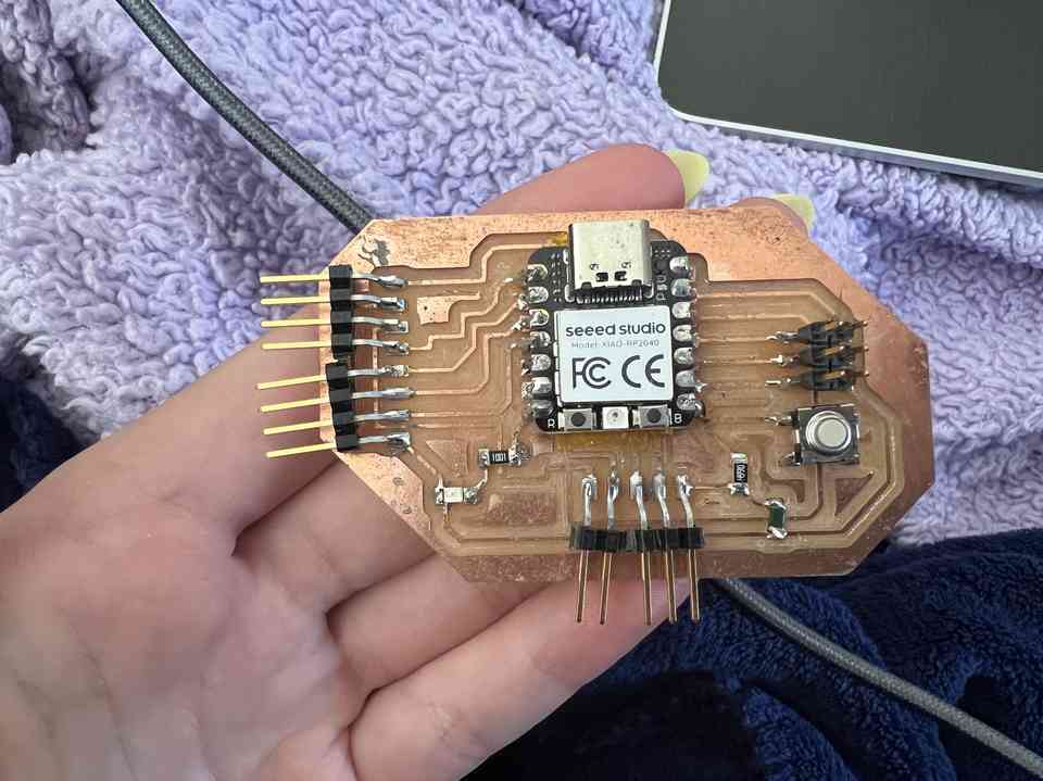
I began this week by soldering a board for a SEEED Xiao RP 2040 chip. I used this website by Adrian Torres as the guide for how to solder the board because this board is based off of his board, but modified by Dr. David Taylor to be in Eagle format. The board’s were milled for uthe students of of Fab Academy group a few hours before this week’s class started by some of our teachers (thank you!!), so we did not have to do that. I began by collecting all of the material specified by the website. This included the following:
- 1 SEEED Xiao RP2040 Chip
- 1 LED
- 1 0 ohm resistor
- 1 499 ohm resistor
- 1 1k ohm resistor
- 1 group of five header pins
- 1 group of six vertical header pins
- 1 group of eight header pins
Once I had these parts, I taped the smallest parts to a piece of paper and labeled them so I didn’t loose them or get them mixed up. With all pieces gathered, I began soldering. I first started with the SEEED chip in the middle of the board. To solder this and all of my components I first melted some solder with some water soluble flux on it onto the pads of the board. Next, I placed the component on top of the board over the pads. I heated up the contacts with my soldering iron to connect the component to the board. If needed I added more solder to the top of the contact. Once the SEEED was on, I soldered the six vertical header pins to the board. Next, I soldered the resistors on, then the LED, and finally the set of five and seven header pins. With everything soldered the next step was to test out the board to see if it works. When I used a USB-C cord connected to a computer USB port, the on board SEEED NeoPixel light began blinking and flashing in multiple colors.
Designing an LED-button board
Simulating The Board
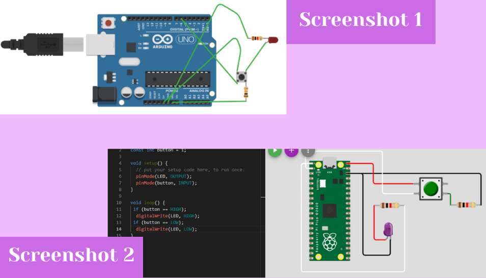
To begin I wanted to model out my design before starting to design in Eagle and KiCAD by simulating it on TinkerCAD. Though TinkerCAD doesn’t have a SEEED chip in it’s library, it does have an Arduino which I can translate over to a SEEED chip and I can also use the same C++ code if I want. I began by dragging out an LED, 2 resistors, and a push button. I want to design something that when the button is pushed it turns an LED on but the LED is not directly connected to the button. I attached the negative leg of the LED to the resistor via a wire drawn between the two. I then connected the positive leg of the LED to pin 7 of the Arduino. For the button I connected the second resistor set to 10k ohm to the button and across from that on the other side of the button I placed a wire connecting it to pin 6 of the Arduino. Then below the 10k resistor I placed a wire to the 5v power of the Arduino (screenshot 1). Once I wrote the quick code to turn the LED in response to the button and began the simulation. The button when pushed did turn on the LED so I proceeded with making my design in KiCAD and Eagle. I did also test in Fritizing but I did not like the UI and how outdated everything looked (screenshot 2). I also preferred TinkerCAD because it will give you a schematic that you can export to Eagle to look at.
 Simulation Download
Ki-CAD
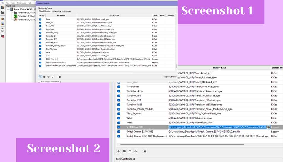
To get started with Ki-CAD I first downloaded and added the SEEED Xiao to the footprints library and schematic library. To do this I used this link to guide me through the process. To begin I downloaded the ZIP library to my files. Then I opened Ki-CAD and in the prefrences from the top bar and then clicked on ‘manage symbol libraries.’ In the window that opened I clicked the small plus sign to add a library (screenshot 1). In the blank row that appeared under the nickname box I typed in “SEEED Xiao rp2040” and in the libary path I hovered over the box so that the books icon appeared. I clicked on the book icon and it opened up in my files I went into the library from my download and clicked on the only file that appeared inside the library “Seeeduino XIAO.lib.” (screenshot 2)
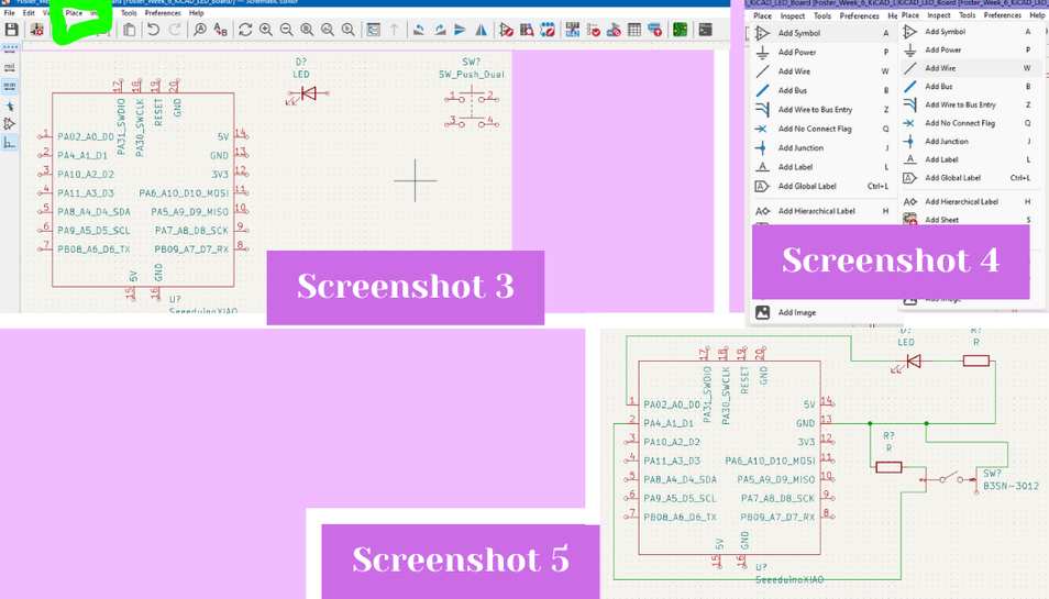
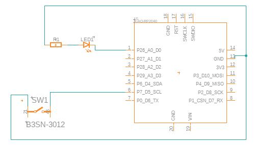
 With that the symbol was imported but I now had to link a footprint to the symbol. Doing this was the same process and for the schematic, but in the preferences I instead clicked on ‘manage symbol libraries’ and followed the same steps as for the schematic but I just clicked on the entire file library instead of a specific library. With that I could being editing my design. I clicked on the schematic file to start making my design. I began by adding symbols to my schematic. To do this I clicked on shortcut letter ‘A’ to activate the symbol selector this can also be done by clicking on “place” (circled in green in screenshot 3) in the top bar and then “add symbol” from the drop down (screenshots 3 and 4). I began by adding the SEEED Xiao rp2040 to the schematic, followed by the LED, then the two resistors, and finally a “SW Push Dual” push button. I had a little bit of trouble picking the button I needed because the symbols and footprints need to be specific to the type of part you have. I knew were were using Omron B3FS 3012 but the schematic only had two button legs when it was supposed to have four so I found a very similar Omron button schematic for the Omron B3SF-100P and instead used that for the schematic and footprint. I downloaded the B3SF-100P from this website and added it to the symbol and footprint libraries the same way I did above. Later I realized the this button was likely included in the Fab libraries which can be downloaded from here and is reccomended for use with KiCAD projects. Once I placed all of my symbols on to the the workspace, I began wiring all of my components together following the design I made in TinkerCAD. I wired up the LED and one resistor to pin 0 of SEEED and to a ground pin. Then I connected the button to the other resistor, a ground pin, and a power pin (screenshot 5).
 Once I felt that everything was wired up correctly I began to assign values to each component and link a footprint if one wasn’t linked already. I did this by right clicking on each component and then hitting ‘properties’ to edit each symbols properties. You can also click on a component and hit shortcut letter ‘E’ to open the properties editor. In the properties menu, I assigned each symbol a number (ie. L1 for LED, R1/R2 for resistors, etc). After assigning a number I assigned a value for the components that needed them. I only had to do this for the resistors which I assigned 383 ohm and 10K ohm for the LED and button respectively. I also had to assign a footprint for the SEEED rp2040 chip and for the button. I did this by selecting the part and clicked the properties menu from the list of options. (screenshots 6 and 7)
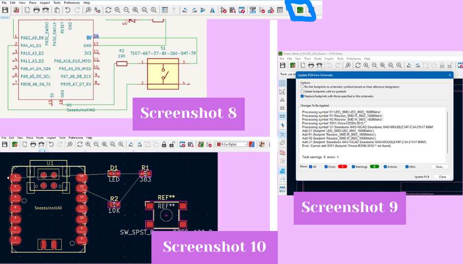
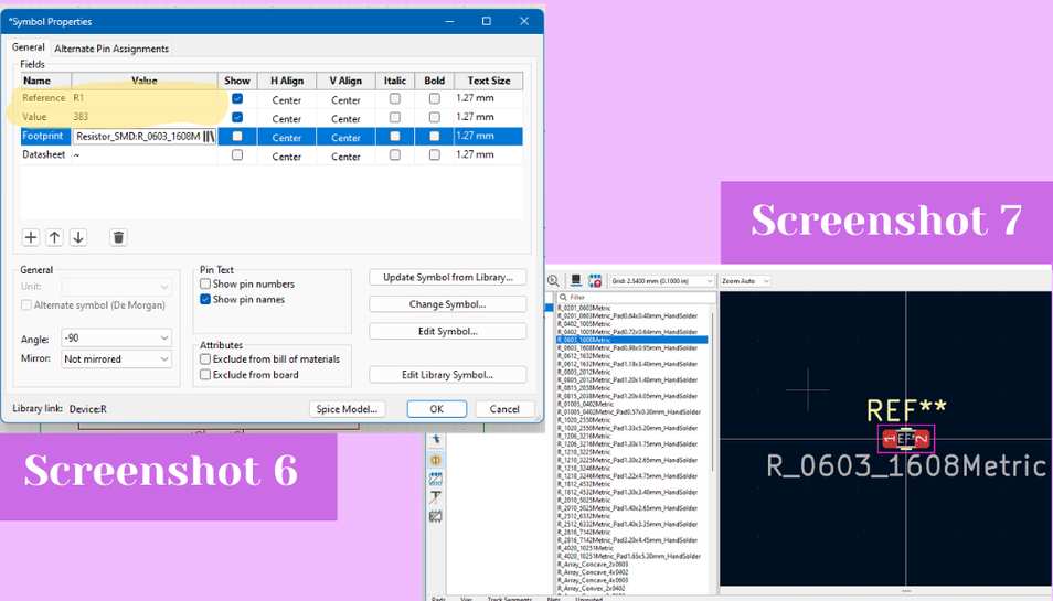 Then I went through the available footprints and selected the one for the SEEED rp2040. Once I selected it, I clicked ok to link the two together. Next, I used the same method to link the button schematic to the button footprint. Once everything was connected and assigned, I saved my design and switched to designing my PCB by hitting the green “open in PCB board editor” button found in the top bar and circled in screenshot 8 (screenshot 8). If you update a PCB from a schematic it will give you a pop up as seen in screenshot 9 (screenshot 9). Once inside the PCB editor I began by arranging my components out and rotating them as needed because they were a but jumbled around (screenshot 10).
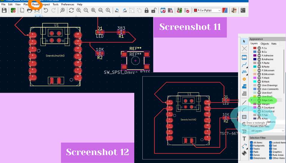
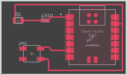
 Once everything was organized how I wanted, I began by routing all of my components together by hitting shortcut letter ‘X’ the command to route a single track which can also be found in the route drop down memu from the top bar as seen in the orange circle of screenshot 11 (screenshot 11). I began routing all of the pads together trying to avoid crossing the traces over one another (screenshot 11). It looks a little jumbled on the final design, but I learned a few weeks later that I could cross a trace without problem using a 0 ohm resistor which I will definitely implement in future board designs if needed. Once I had all of my traces done I switched the layer of the board I was working on to ‘Edge.Cuts’ in order to set the shape of the board by clicking on it from the right hand side bar which can be seen in the green highlights of screenshot 12 (screenshot 12). I didn’t want anything fancy so I went with the rectangle. I drew this out by selecting the rectangle box from the right side bar (blue highlights of screenshot 12) menu and drawing out the rectangle (screenshot 12).
 Once I was done with this, I saved my design to complete KiCAD.
Eagle CAD in Fusion 360
To get started in Eagle CAD, which I had never used before, I found a succinct Eagle tutorial from Autodesk which can be viewed here there are multiple short videos which explained how to create a schematic and PCB in Eagle.
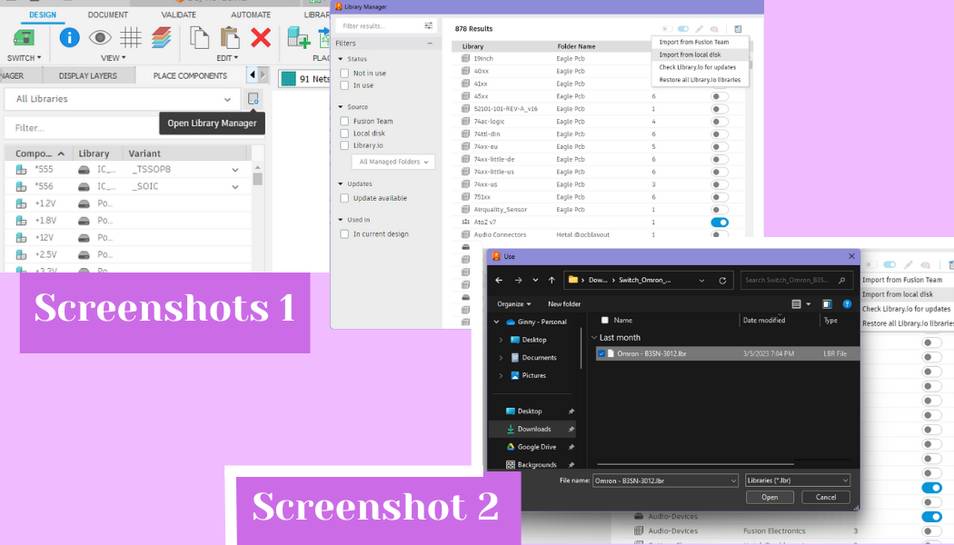
To begin designing in Eagle first I had to get to Eagle from inside Fusion 360. I did this by clicking on the file button from the top left corner and then selecting ‘new electronics design.’ This opened up the three tabs above the top bar and to begin my design I opened up the schematic tab. The first thing I did was place components onto the schematic workspace using the button circled in purple in screenshot 3 (screenshot 3). To do this I went through the libraries on the left side and dragged out the components I wanted onto the workspace. I uploaded a library for my button by clicking on the library manager in the right of side panel, then I clicked the small import button inside the library manager tab to import a library (screenshot 1). Next, I chose to import a library from local disk, and opened it, then I had to go into the library manager and toggle the library on to be able to access it (screenshot 2).
 I dragged out 1 SMD button, a SEEED Xiao RP2040, 2 SMD LEDs, and 1 SMD resistor (screenshot 4).
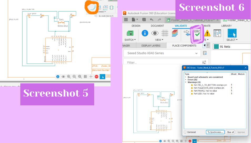
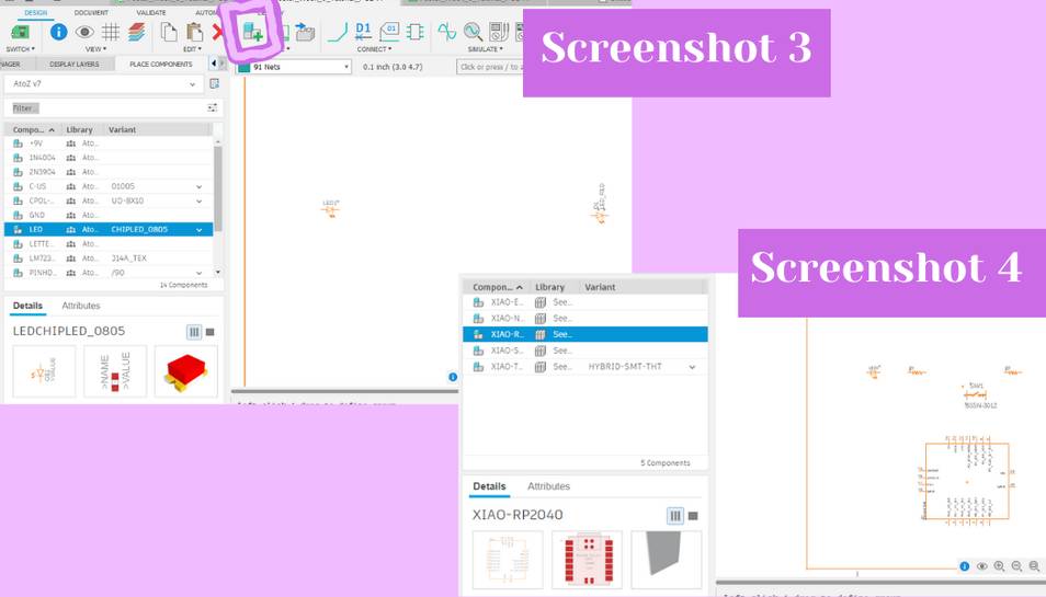 I then arranged them onto the workspace and began placing wires between the components using the net tool circled in orange in screenshot 5 (screenshot 5). I did an electrical rules check on my design by switching to the validate tab in the top, and then clicking on the button that says “ERC” with a green check which is circled in purple in screenshot 6, inside the pop up I ran the check and it said that I had no red errors so I was good to go (screenshot 6).
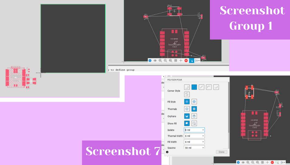
 Once I had placed wires between the necessary components, I switched into the PCB workspace. I did this by clicking the upper left hand “switch” button which if hovered over says switch to PCB. Inside the PCB workspace I began by moving over all of the components onto the bottom left dark grey workspace (screenshot group 1). Then to make the workspace smaller because that would be the board size, I clicked on the top edge and dragged it down to the top of my components. I did the same for the right hand side of the grey workspace. When it is dragged in, green lines appear to show you where the intended new lines would be. From there, I rotated the footprints as needed until everything looked like it should. From there according to the video tutorial I had to do a polygon pour. I did this by dropping down the polygon tab and clicked on the “polygon pour” option and clicked ok on the dialog box that opened (screenshot 7).
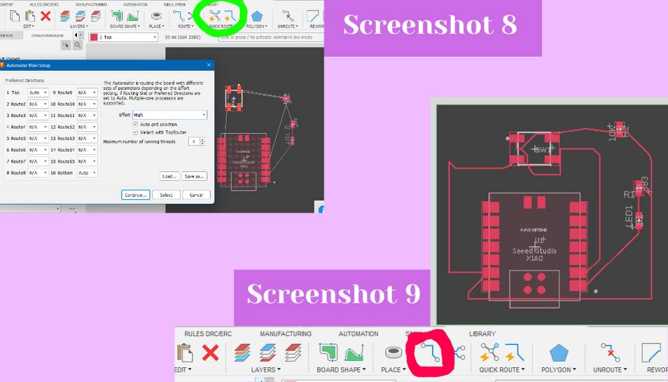
 I am still not clear on why this needs to be done in order for routing to work because KiCAD does not have this but I am just going with it. From there I could route. There is a quick routing feature which I briefly tried but it didn’t come up with a way to not have to print on the front and back of the copper board (screenshot 8). Instead I decided to route by hand and to do this I clicked on shortcut letter “R” to activate the manual routing tool which can also be activated by clicking the button circled in red in screenshot 9 (screenshot 9). I then connected the pads of the components like they were in the schematic (screenshot 9).
 The PCB was also constrained so that you could only connect the pads/legs that you had connected in the schematic. Once everything was connected, I was essentially done with the design and could export it by clicking the file button in the top left and then the export button. You can find the file below.
Milling A Board
I chose to mill my Eagle board, but I first made some modifications to the design because since making the original I have learned some more tricks to make Eagle easier to use. I made the traces bigger, and I also simplified the design by making the button an independent input and the LED an independent output that are not directly connected. I still however followed the same process that I did above.
Schematic
PCB design
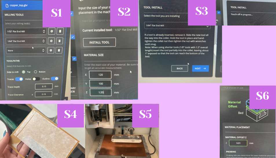
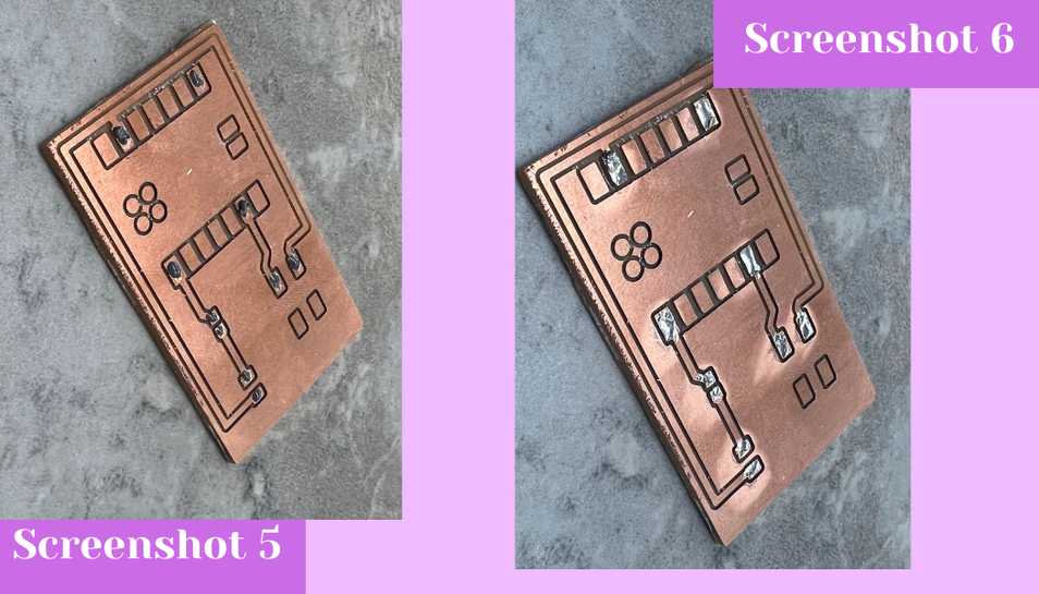
I started by opening the Bantam Milling software. I used an Othermill Pro milling machine for this board. Inside the Bantam Milling software I first uploaded my gerber file for the copper top and the profile into the software. Next, I selected what bits I was going to use for the milling job. I went with a 1/32” two flute upcut endmill and a 1/64” two flute upcut endmill which I selected in the milling tools section (S1). Next, I generated the gcode for it and then changed the material size. I used calipers to measure the copper I was using and then inputs it’s dimensions (120 x 100 x 1.55 mm) into the material size dialog box (S2). From there I input the material offset which is 0.01mm because of the tape we use to affix the FR1 to the bed. Next, I installed the bit by unscrewing the installed bit using two wrenches and then inserting a 1/64” endmill bit. From there I went through the tool install dialog boxes by first hitting the bit I was installing (S3, left photo) and then letting it touch off the bed (S3, right photo). With that done, I used Nitto tape to tape the bottom of the FR1 to the bed (S4 and S5).
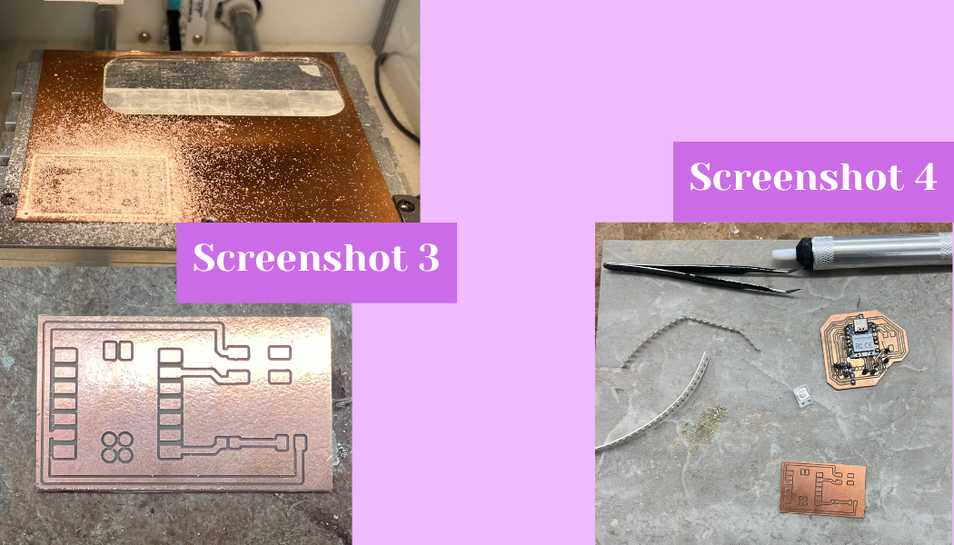
 From there I started the file to mill and waited for it to finish. I had to change the tool a quarter of the way through the job, and it paused to allow me to switch to the 1/32” endmill bit. After it was done I used a vacuum to suck up all of the copper shavings leaving me with my board (screenshot 3). I then got out the following tools to solder (screenshot 4):
- 1 pair of tweezers
- 1 solder sucker
- 1 SEEED Xiao RP2040 (soldered to another board because our lab ran out and I had to scavenge)
- 1 orange SMD LED
- 1 330 ohm SMD resistor
- 1 Omron B3SN button
- 1 tube of solder paste
Note: I had to use a SEEED Xiao RP2040 that was originally soldered to another board because our lab had run out of new SEEEDs and thus I had to scavenge around for a SEEED not being used. I de-soldered from its original board using a solder sucker
From there I started the file to mill and waited for it to finish. I had to change the tool a quarter of the way through the job, and it paused to allow me to switch to the 1/32” endmill bit. After it was done I used a vacuum to suck up all of the copper shavings leaving me with my board (screenshot 3). I then got out the following tools to solder (screenshot 4):
- 1 pair of tweezers
- 1 solder sucker
- 1 SEEED Xiao RP2040 (soldered to another board because our lab ran out and I had to scavenge)
- 1 orange SMD LED
- 1 330 ohm SMD resistor
- 1 Omron B3SN button
- 1 tube of solder paste
Note: I had to use a SEEED Xiao RP2040 that was originally soldered to another board because our lab had run out of new SEEEDs and thus I had to scavenge around for a SEEED not being used. I de-soldered from its original board using a solder sucker
With my SEEED de-soldered I could proceed with my board soldering.
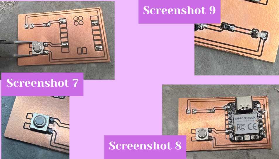
 I started by using a tube of solder paste to put a little on each pad I wanted to solder something to (screenshot 5). I then took my soldering iron and touched it to the solder paste and it turn from paste into tin metal (screenshot 6).
 I then used my tweezers to hold the button over the pads (screenshot 7, top), and my soldering iron with a little solder on it and touched the soldering iron to the area between the button pad and the board pad to form a solder connection between the two (screenshot 7). I did this for the two pads of the button, and then I did the same thing to solder the SEEED RP2040 to the copper (screenshot 7, bottom and screenshot 8). I next used tweezers to affix the LED and resistor to the board by holding each component to the board and heating up the solder around the edge of each side of the component (screenshot 9). This left me with my soldered board.
Board Testing
I then moved onto programming the board using a simple button code adapted from the Arduino “button” example code. I changed the button pin to 7 as that was the pin that I had the button connected to, I also changed the LED to 26 as that was its pin. I uploaded the code to the SEEED RP2040 using Arduino and it worked! The LED would turn on when I pressed the button as you can see in the video below.
// Modified by Ginny Foster for Fab Academy 2023
// Originially made by:
*/created 2005
  by DojoDave <http://www.0j0.org>
  modified 30 Aug 2011
  by Tom Igoe

  This example code is in the public domain.

  https://www.arduino.cc/en/Tutorial/BuiltInExamples/Button
*/

// constants won't change. They're used here to set pin numbers:
const int buttonPin = 7;  // the number of the pushbutton pin
const int ledPin = 26;    // the number of the LED pin

// variables will change:
int buttonState = 0;  // variable for reading the pushbutton status

void setup() {
  // initialize the LED pin as an output:
  pinMode(ledPin, OUTPUT);
  // initialize the pushbutton pin as an input:
  pinMode(buttonPin, INPUT);
}

void loop() {
  // read the state of the pushbutton value:
  buttonState = digitalRead(buttonPin);

  // check if the pushbutton is pressed. If it is, the buttonState is HIGH:
  if (buttonState == HIGH) {
    // turn LED on:
    digitalWrite(ledPin, HIGH);
  } else {
    // turn LED off:
    digitalWrite(ledPin, LOW);
  }
}
Case in Fusion 360
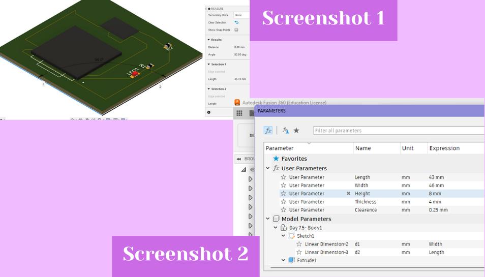
To build a case for the board I made in Eagle, I began by measuring the 3D mockup of my board by clicking on the file and then inside I hit shortcut letter “i” to activate the measure feature, which can also be found inside the inspect dropdown. From there I clicked on the lines of the PCB mockup to measure how long, wide, and tall it was (screenshot 1). With those measurements I could then proceed with my case. I chose to copy a document that I had made during Fab Academy Prep on how to make a sliding dovetail box, and I followed this tutorial when I made the original box. Once I copied the document, I went in to the user parameters which were implemented in the design of the box, and began updating the dimensions according to the measurements I took from the measuring I did above. This came out to 43 mm length x 46 mm width and 8 mm in height (screenshot 2).
 From there I added a hole in the lid so a user could access the button and LED. I did this by clicking on the create drop down, and then hitting the create a sketch button. From there I clicked on the rectangle button and drew a rectangle on the top of my box lid (screenshot 3). For ease of use and comfortability I filleted the hole in the box lid to there were not any jagged edges. I did this by hitting shortcut letter “f” but the fillet tool can also be found in the modify dropdown menu. Next, I filleted by 1.2 mm which I felt was enough (screenshot 4).
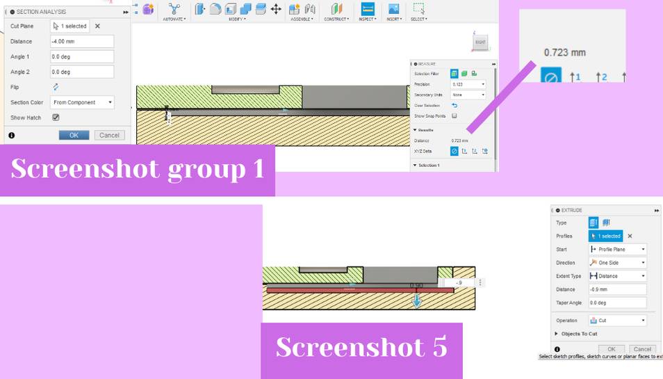
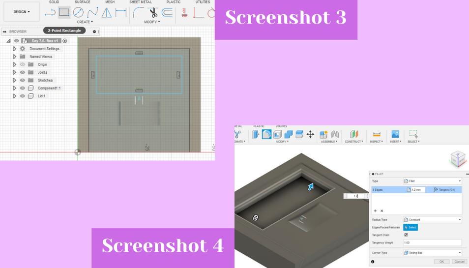 Next, I used the section analysis tool so I could measure the inside thickness of the box. I did this by hitting the inspect drop down, and then I hit the section analysis tool. From there I selected the side plane and dragged the blue arrow in until I could see the inside of the box. Then I could use the measure tool by hitting shortcut letter “i” to measure the inside thickness, this measurement came out to ~.7mm which was less than the box thickness, so I knew I needed to increase the inside dimensions of the box (screenshot group 1 for section analysis and measuring). I did this by keeping the section analysis on and the by hitting shortcut letter “e” for extrude which can also be found in the create drop down. From there, I typed in “-0.9” mm to lower the ‘floor’ of the inside box by that much and allowing me 1.6 mm of height inside the box (screenshot 5). My design files can be found below.
Reflection
Personally, this week I learned that I much prefer EagleCAD to KiCAD because EagleCAD offers better integration. EagleCAD allows you to more easily swap between schematic and PCB, the placing of symbols and organization of symbol libraries is superior to KiCAD, and Eagle allows you to see a 3D model of your board. KiCAD also looks about 5 years older the Eagle does, and I think that personally it is harder to navigate compared to Eagle. For those reasons I am going to switch over to using EagleCAD for any PCB designing I might need to do in the future.