6. Electronics design
![]()
Planning
Tasks - Must
- In group - Use the test equipment in your lab to observe the operation of a microcontroller circuit board
- Individually - Redraw one of the echo hello-world boards or something equivalent
Tasks - Nice to
- Redesign the sun tracker circuit in KiCad
- Revisit the flexible heating PCB idea
Execution
Group assignment - Measure with Lab equipment
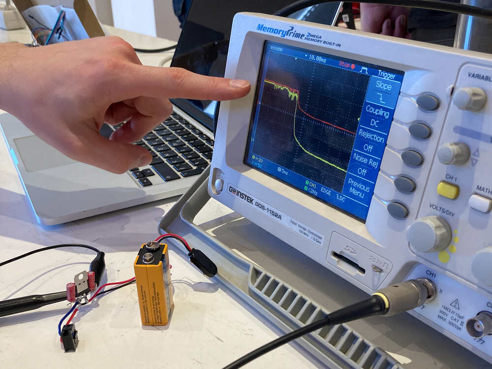
Together with Saco and Jonathan we experimented with the oscilloscope. We started by measuring the voltage of a 9V battery.
Voltage scale
We measured the battery voltage with both channels. CH1 was showing the expected 9V but CH2 was showing ~500V. We checked the gain switch on the probes but they were both set to 1X. Why are the two channels not measuring the same voltage then?
Henk showed us that it’s possible to set a voltage scale in the menu. Once we changed the scale of CH2 from 50X to 1X the two channels were both showing 9V as expected.
Next we wanted to measure something more interesting that justifies the use of an oscilloscope. We measured the charge and discharge of a capacitor. It took us some tries before we got the trigger settings right but once we did we were able to visualize charge/discharge curves.
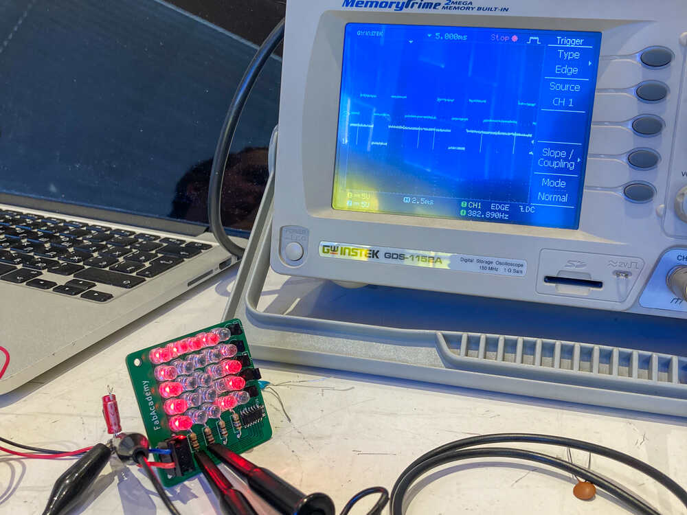
In the Fab Academy bootcamp we made a soldering exercise where we created a led matrix that can show our names. We used the oscilloscope to measure how the led rows switch on/off to show different letters.
KiCad
During our local lesson Erwin gave us a short introduction into KiCad. Based on his explanation I changed the following settings:
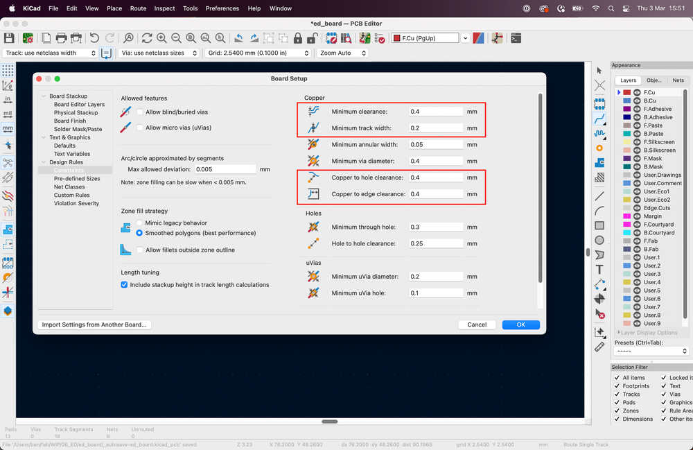 Configure track width and clearance constraints based on the design rules of our fabrication process. These settings will be taken into account when running
 Inspect > Design Rule Checker
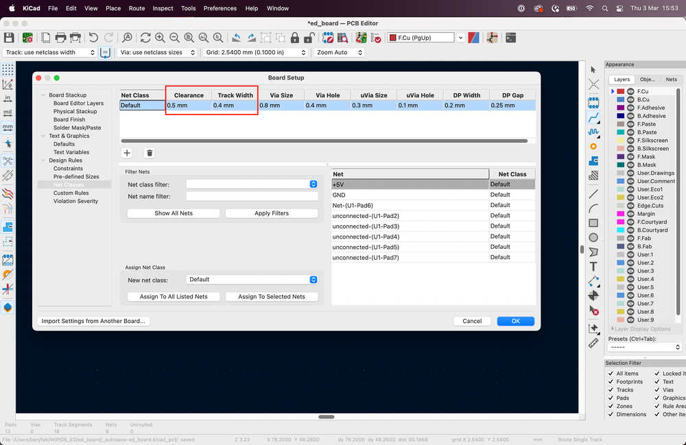 Set default clearance and track width. When drawing traces they will have the width I did set here by default.
Individual assignment - hello world board 
Design
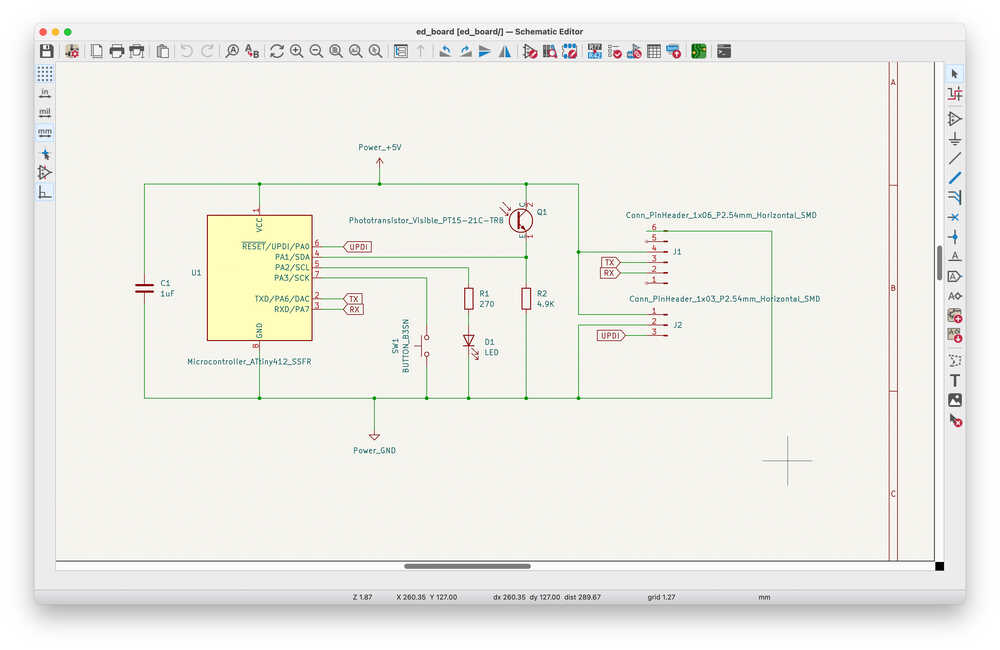
I designed a small board with the ATtiny412 and the following components:
- UPDI header
- Serial header
- Green LED with current limiting resistor
- Button
- Capacitor to smooth operation voltage
- Phototransistor with resistor
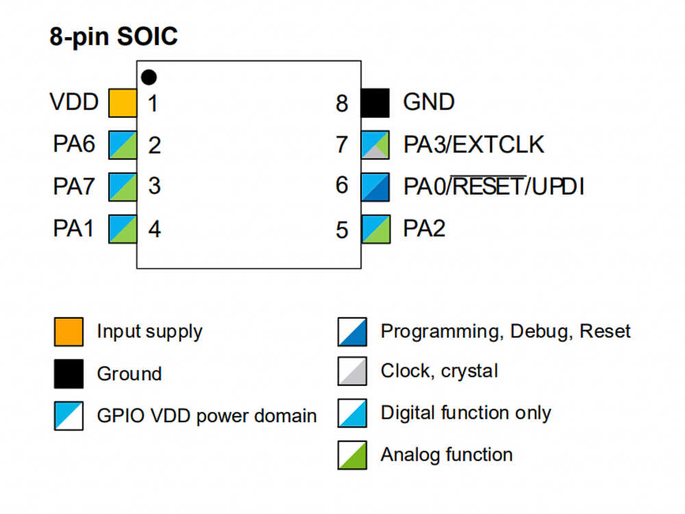
This image from the AtTiny datasheet shows the functions of the various pins.
By looking at the labels in the KiCad component and the pin functions above it was clear where to connect power, ground, UPDI, TX and RX. Once this connections were made I was left with PA1, PA2 and PA3. As this pins all have digital and analog functions I can connect the led, button, and phototransistor to any of them.
Once I completed the schematic I switched to the PCB view and imported the components with F8 (Update PCB with changes made to schematic).
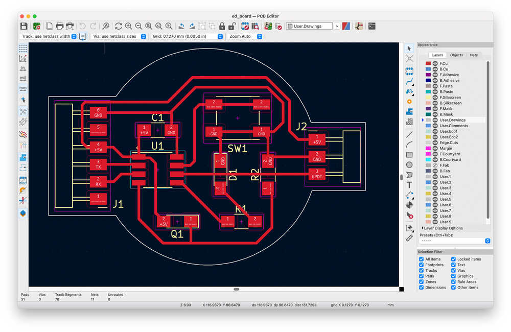
I did draw the traces on the F.Cu layer and the board outline on the Edge.Cuts one.
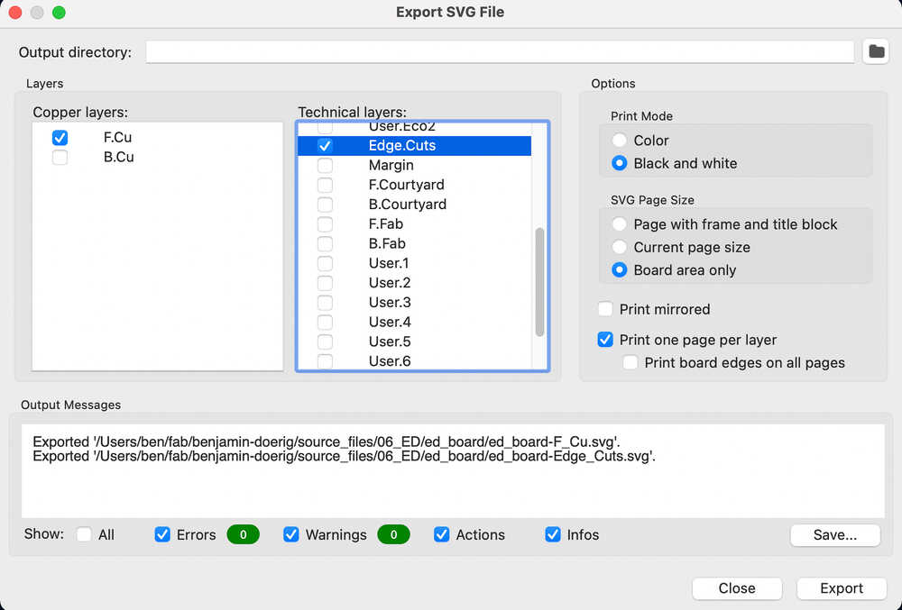
I exported SVGs for traces and outline by going to File > Export > SVG and using the settings in the image above.
Production
I prepared the milling machine and mods as described here.
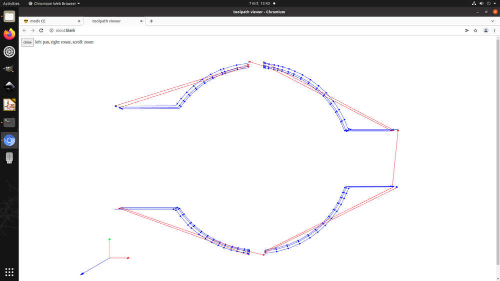
Connection between mods and the machine
At first I couldn’t get the connection between mods and the machine to work. I did press the move to origin button before closing and reopening the websocket serial socket and port. It’s important to close and open socket and port before doing anything else
Mods expected the traces to be white and the background black. The export from KiCad was the other way around but that’s easy to adjust be clicking Invert in the Convert SVG image block.
Cut depth
When adjusting the cut depth for the traces I made a typo and set it to 0.5 instead of 0.05. Once I started the mill it did cut much deeper than intended and the milling bit broke.
SVG image dpi
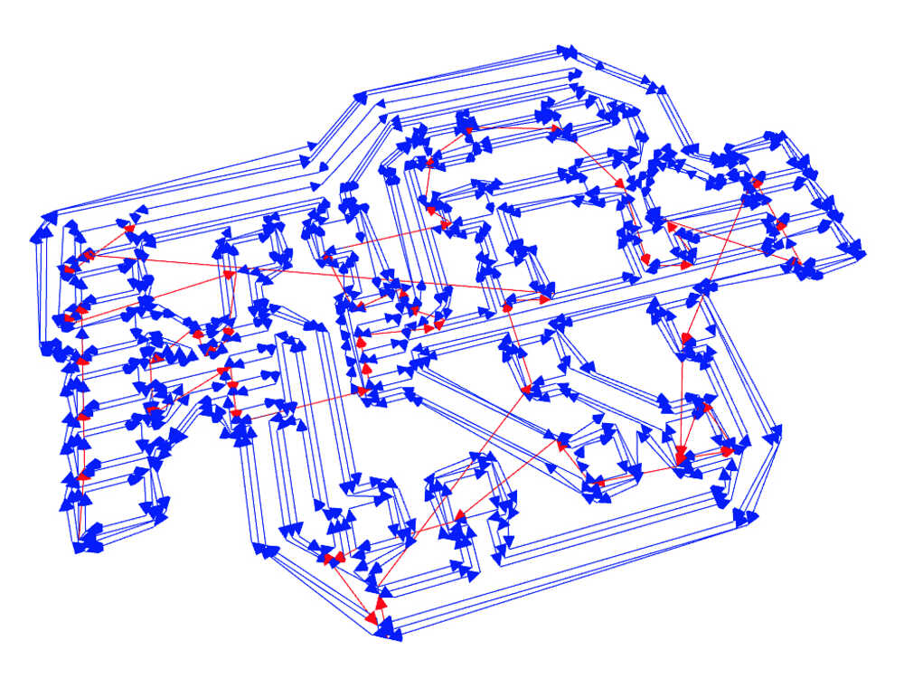
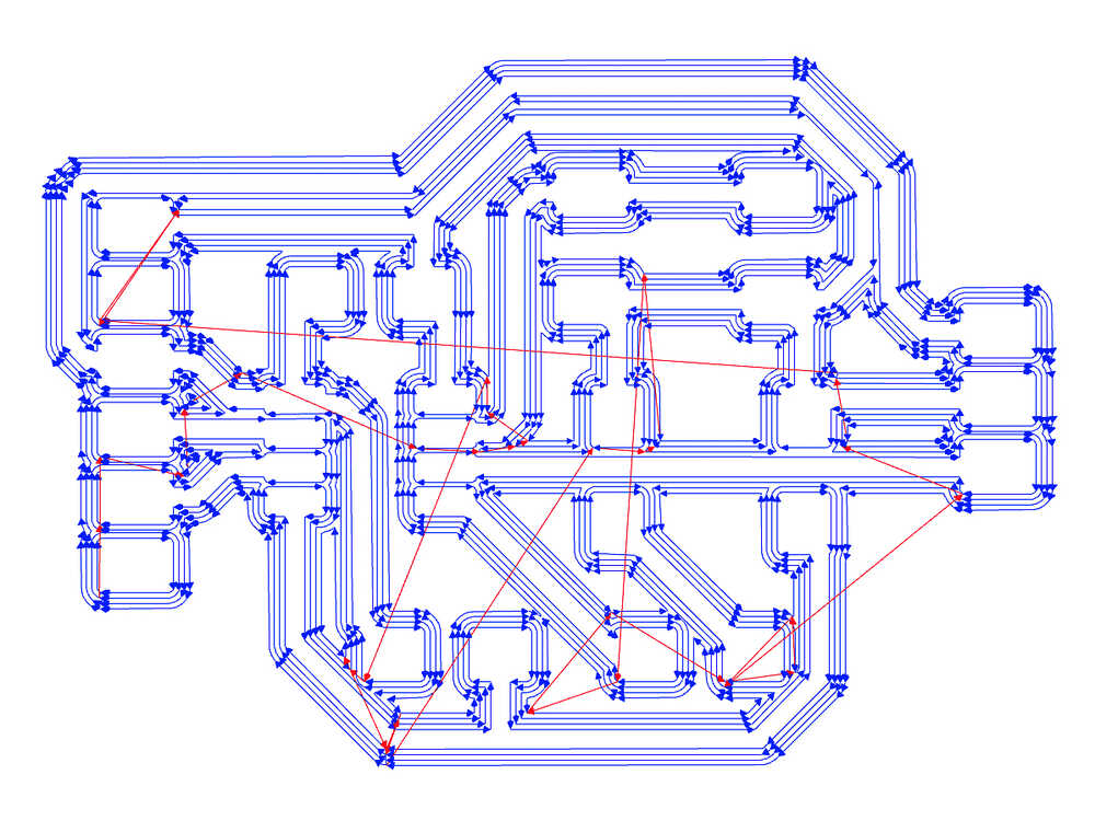
Once I started successfully milling traces I realized that they didn’t look as expected. The toolpath image confirmed that there was something off. I wasn’t sure why this was happening but Henk knew straight away that I had to adjust dpi in the convert SVG image block. Setting dpi to 1000 fixed the issue.
This is how the toolpath looked with dpi 100:
And this is how it looked once I adjusted dpi to 1000
The outline SVG exported from KiCad is a line but mods expects a white inside of the board with a black background. I adjusted the outline SVG in inkscape by filling the inside of the board in black and later inverting black/white in mods.
No space around outline
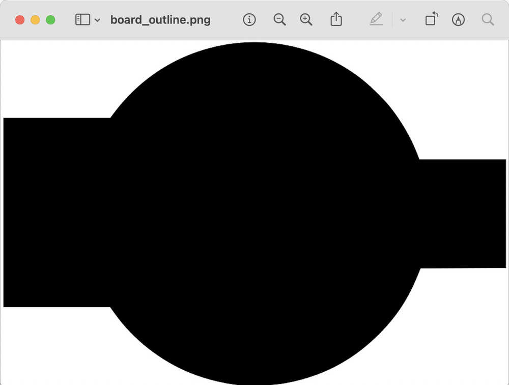
There is barely any space/background around my outline. It turned out that mods didn’t interpret correctly the parts where the board is close to the edge of the image.
I fixed this by making the outline image bigger and keeping the outline centered (+10 mm in both X and Y). Then I adjusted the origin of the milling machine accordingly (-5 mm in X and Y). It would be easier to adjust both the traces and outline images beforehand to avoid changing around the machines origin but I did it this way as I did already mill the traces.
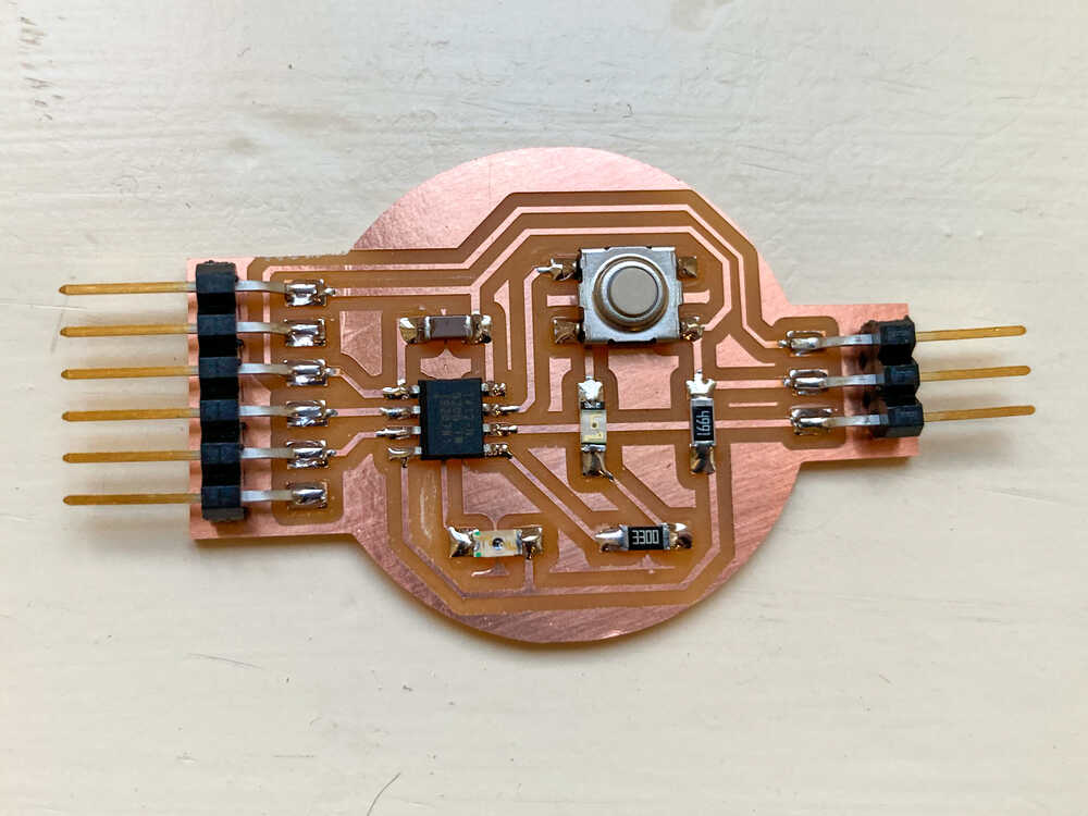
Once I fixed the outline I managed to complete the milling successfully. This is the board once I did solder all the components on it:
Redesign sun tracker 
In previous weeks I built 2 versions of a sun tracker.
- V1 was a laser cut structure with a circuit on a stripboard
- V2 was a laser cut structure with a vinyl cut circuit sticked to the structure
- This week I want to redraw the PCB in KiCad and produce it on the milling machine.
While working on my individual assignment it was a bit tricky to get the boards outline right:
- KiCad isn’t the most intuitive tool to draw outlines that are a bit more complicated than a square
- The KiCad outline SVG export needs to be adjusted before being usable for mods
The outline of this board isn’t going to be straight forward either and I did therefore explore other approaches to deal with the outline by using the ability of KiCad to import vector graphics (PCB editor: file > import > Graphics)
import DXF from fusion
My first attempt was to export DXF from a fusion 360 drawing and importing it into KiCad. I manage to export and import but the graphic was malformed in KiCad. Not sure why. Maybe fusion and KiCad use different versions/flavours of DXF?


Unfortunately fusion can’t export SVG natively but it’s possible by installing the Shaper Utilities plugin. Once I installed the plugin I was able to export faces of bodies a SVG. That’s pretty handy :-)
fusion SVG export in KiCad
The SVGs that I exported from fusion with the Shaper Utilities plugin looked fine when I opened them in inkscape but once I imported them into KiCad they were looking different.

It turns out that the shape is correct but the stoke line is super thick. It looks like the line width is not explicitly defined in the SVG and kicad sets it to 10mm.
Once I opened the SVG in inkscape and set the stroke width it imported correctly in KiCad. Nice! That means that I can create a PCB outline in KiCad based on a design in fusion :-)
I decided to proceed in the following way for my sun tracker PCB:
- Export outline SVG from fusion
- Add some helper lines to SVG in inkscape to make it easier to place the components in the right places
- Import SVG into KiCad on the
User.Drawingslayer. When putting it on theEdge.Cutslayer KiCad gets confused by the construction lines - Design PCB in KiCad
- Export
F.Cuas SVG - Merge
F.CuSVG andoutlineSVG exported from fusion in inkscape - Inkscape: Create multiple layers for
traces,holes,cutoutsandoutline - Inkscape: Make page a little bigger to create background/space around the objects (needed by mods as described earlier)
- Inkscape: Export one PNG for each layer
These are the resulting traces, holes, cutouts, outline and more outlines for the sun shade.
I did mill them in this order. The traces with the 0.4 mm mill and the rest with the 0.8 mm one.
![]()
![]()
![]()
![]()
![]()
Tight joints & cut depth
Once I completed milling the boards I realized that my joints didn’t fit as they were too tight. My design was for 1.5 mm thick material but the cutouts turned out to be about 1.45 mm and the material up to 1.55 mm. I made them fit be sanding them down a bit. If I will mill joints in the future I will design them to be a bit looser.
Most of the traces were milled nicely but in one corner the mill didn’t go completely through the material. I could have re-run the milling with a slightly deeper cut depth but I instead decided to just fix it with the knife.
![]()
Once I completed sanding the joints I removed some copper from the shades to avoid shorting the traces of the circuit. Then I soldered the components on it and this is how it looks once completed:
![]()
Revisit flexible PCB heater 
I’ll will continue with my previous attempt to make a flexible circuit that can be used as a heater.
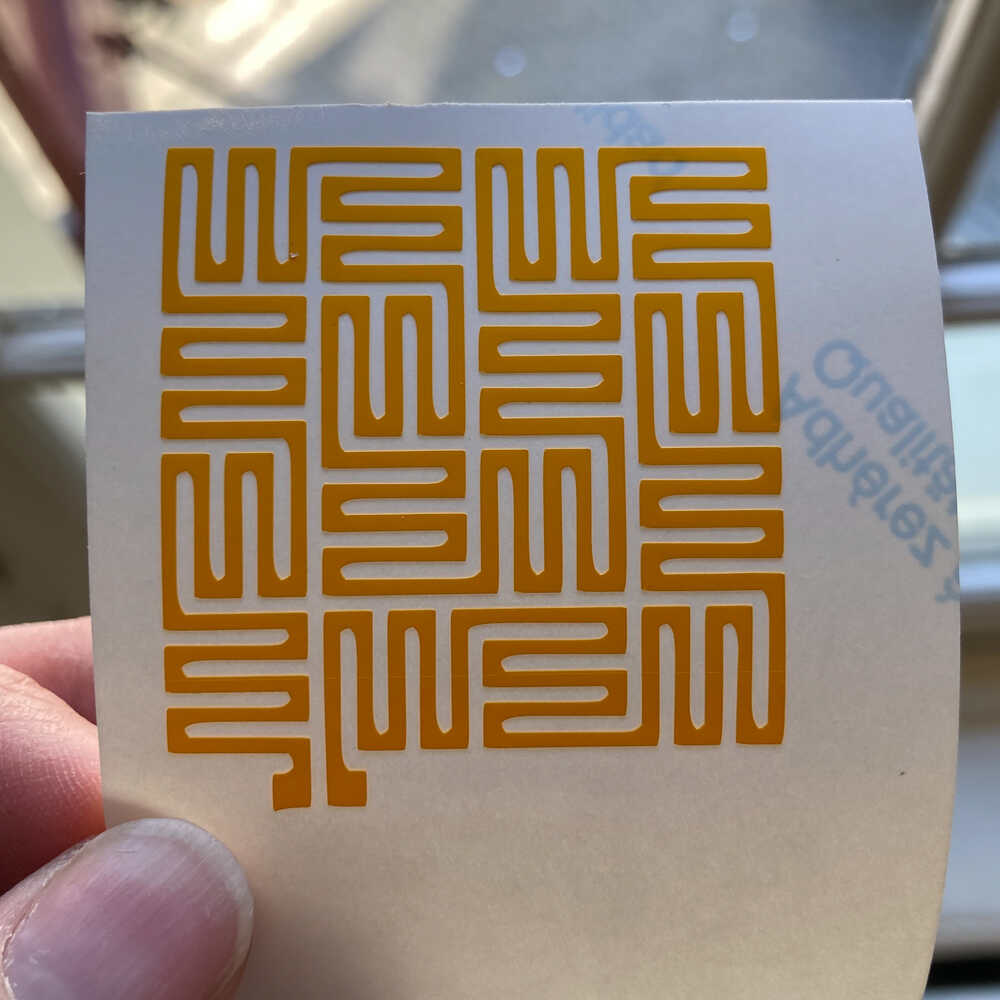
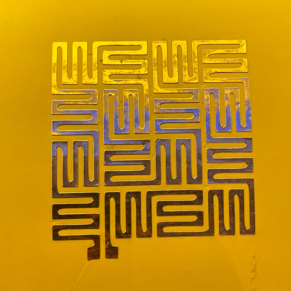
Last time I had the problem that the SVG exported from OpenSCAD was not really suitable for mods with the effect that too many cutting lines were generated.
To make the SVG work for mods I made the following changes using inkscape:
- Remove stroke
- Change fill color from grey to black
- Make image slightly bigger to have some background all around the object. Before object was getting up to the edge.
Once I made the changes I managed to make a successful test cut with vinyl. Next I tried with copper and it turned out well too :-)
Now that I had a circuit I tested if it can really be used as a heater.
To estimate what voltage to power it at I did measure the circuits resistance. I wasn’t able to get an accurate measurement. I tried multiple multimeters and I got results between 0 and 4 ohm. At that point I decided to just power it at 2V and see what happens.
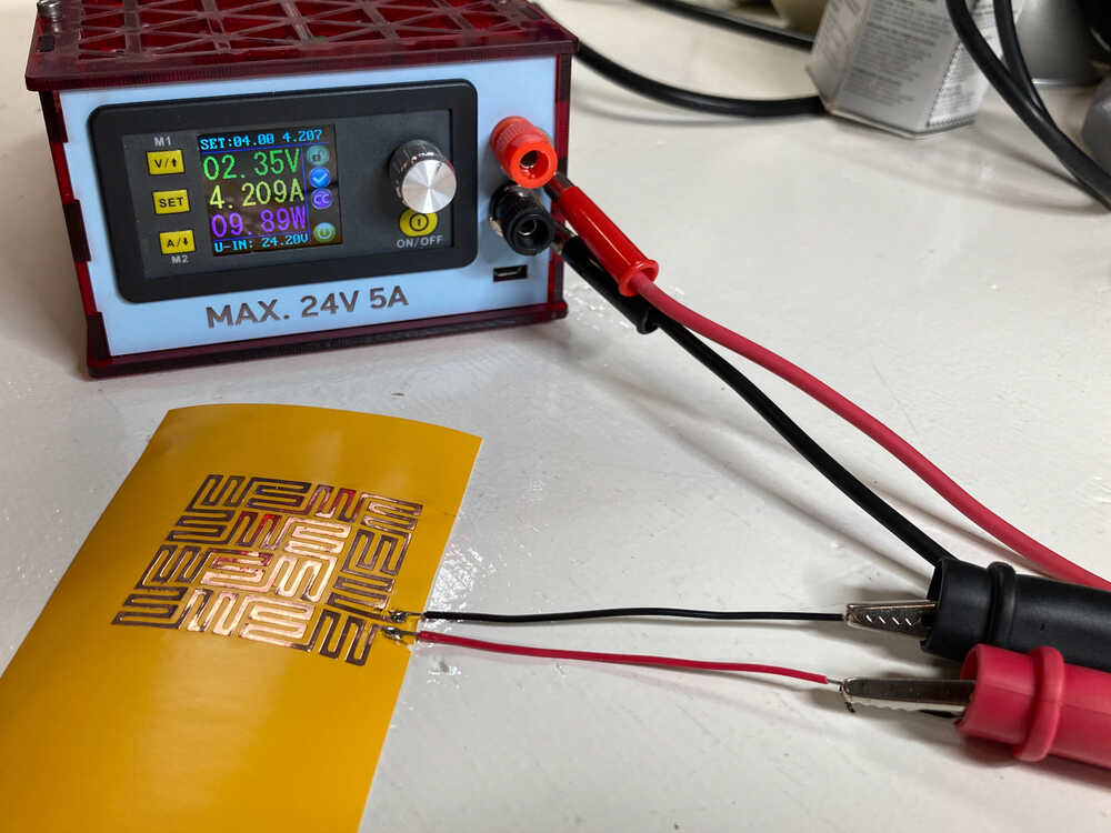
2V turned out to be a pretty good value to start with. The circuit heated up quite quickly without burning or melting.
Once I knew that the circuit was heating as expected I decided to stick it on a jar to see if it is possible to heat water with it.
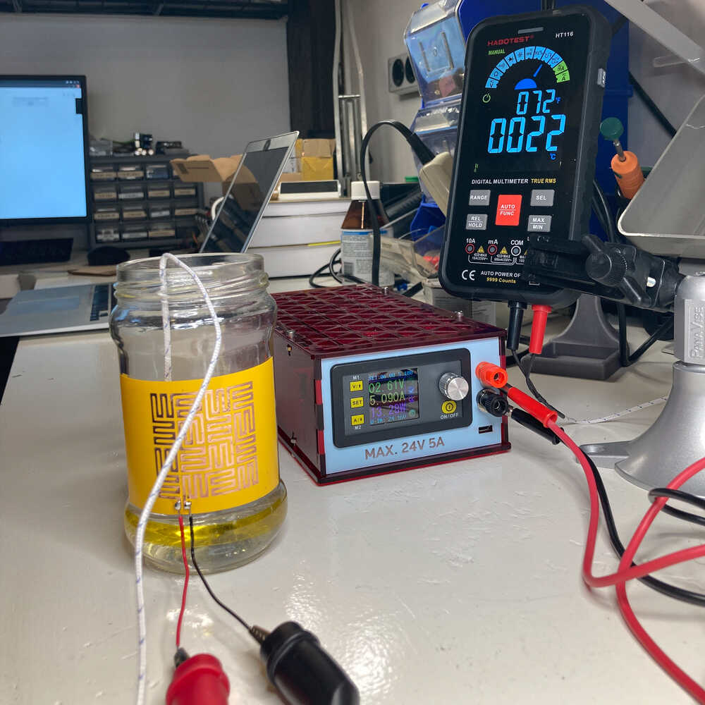
It works but it’s really slow. It took 10 min to heat a small amount of water from 13 to 22 degrees.
While heating the water the circuit was at about 45 degrees. It turns out that it’s probably not the best way to keep my coffee warm as the cup would get too hot to touch and the heat transfers only slowly to the liquid.
Retrospective
This week was a lot of fun. I enjoyed designing circuits in KiCad: The program is easy to use and trying to find a way to position components and traces well is a bit like solving a puzzle. The only thing which was not straight forward and needed a bit of finding out was how to deal with board outlines. I’m happy that I managed to pick up and improve the sun tracker and the heater circuit I started in earlier weeks.
This week I made PCB’s with copper traces on one side of the board (single layer PCB). Later on I made a 2-layer PCB for my final project.