Electronics Production | Week 05
Group Assignment #2: Electronic Production
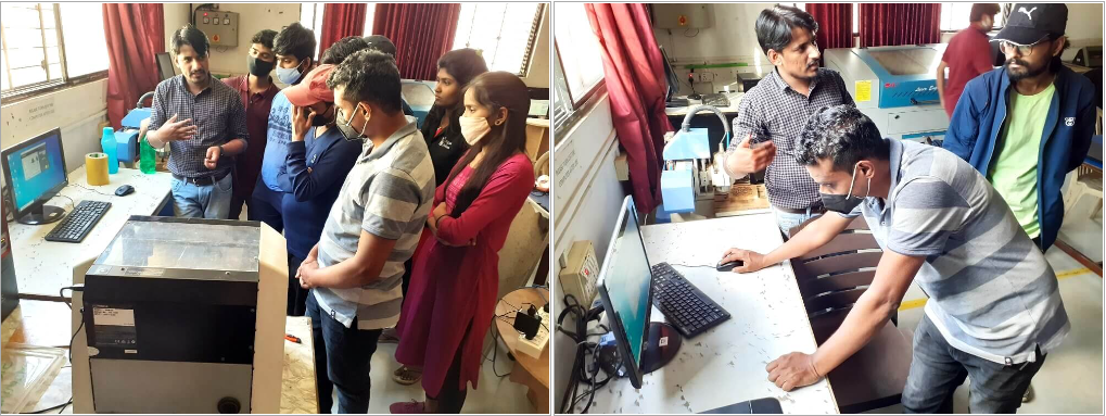
Objectives of this Group Assignment:
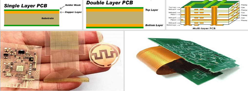
Types of PCBs
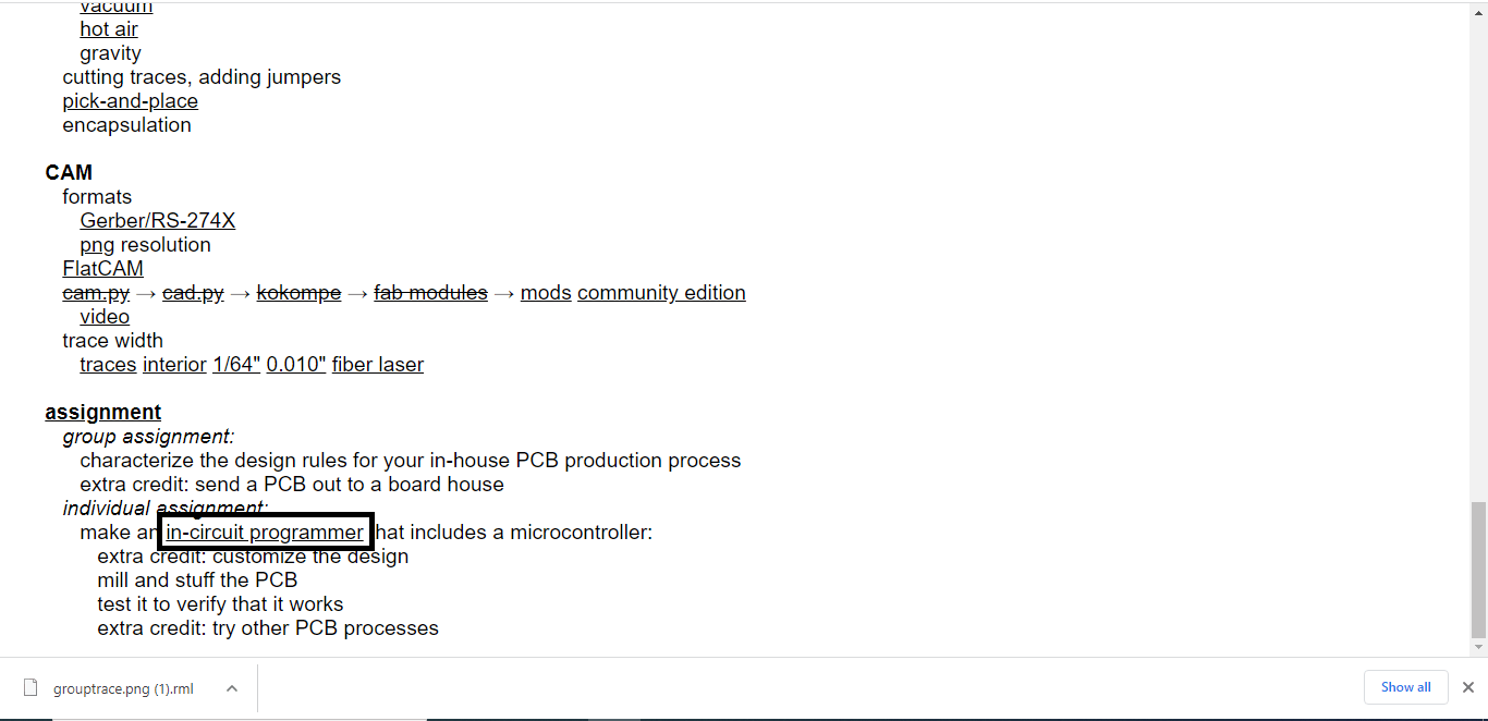
PCB Fabrication (Process, Material, Machine and Tools)
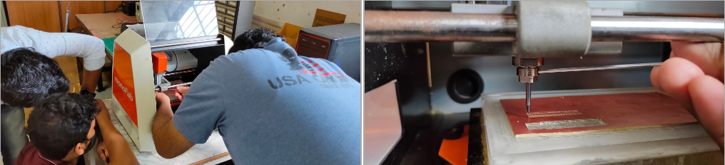
Machining (Milling) for PCB Fabrication
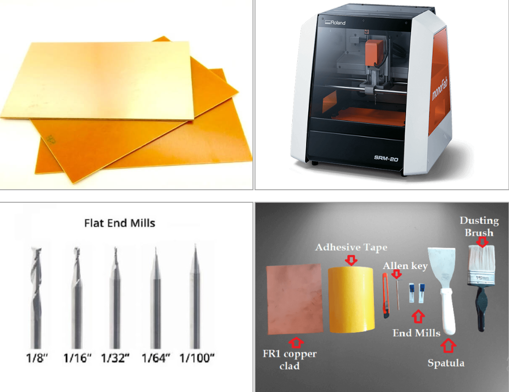
Material, Machine and Tools used in PCB Machining (Milling)
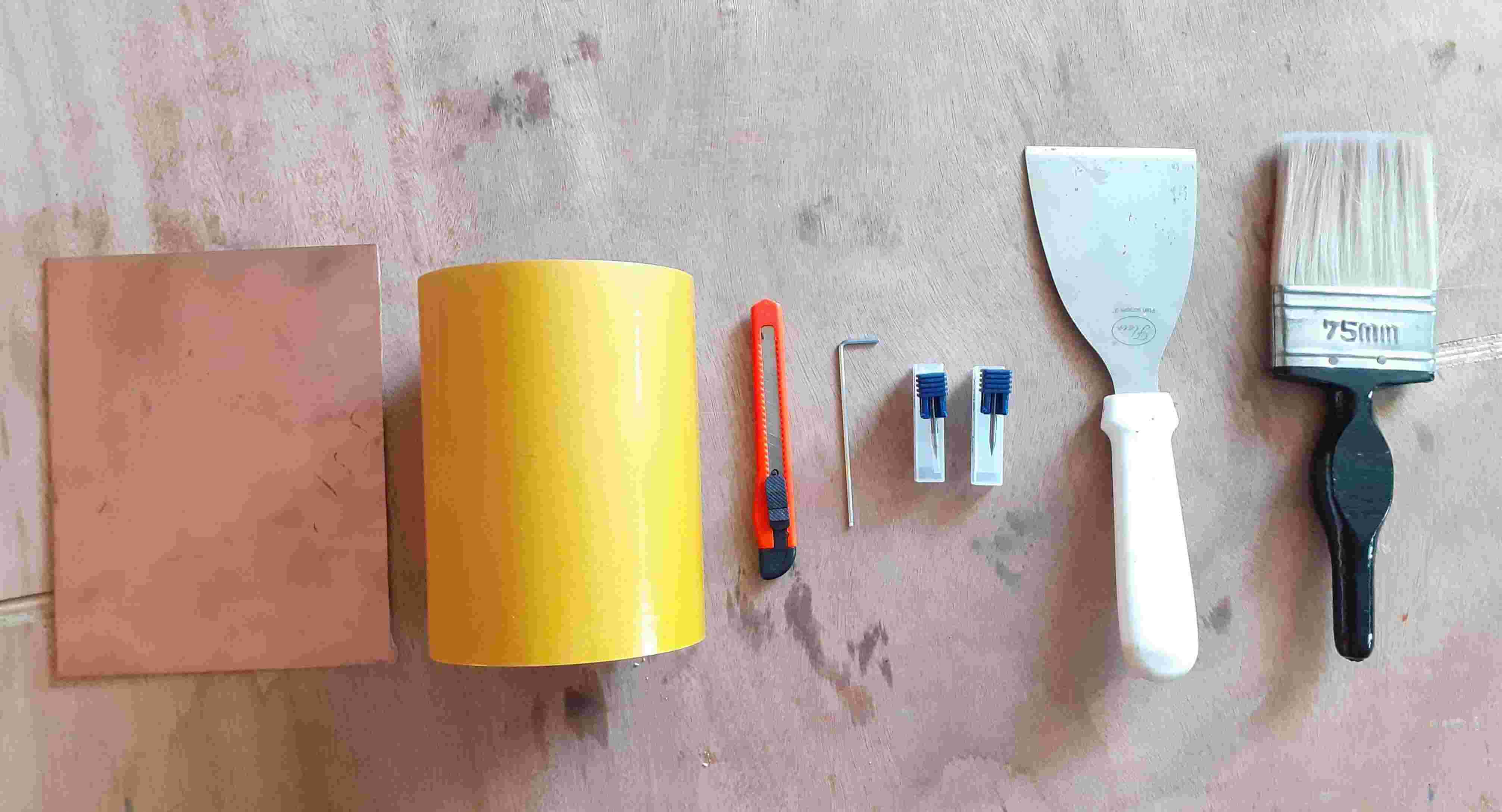
Material:
Machine:
Tools:
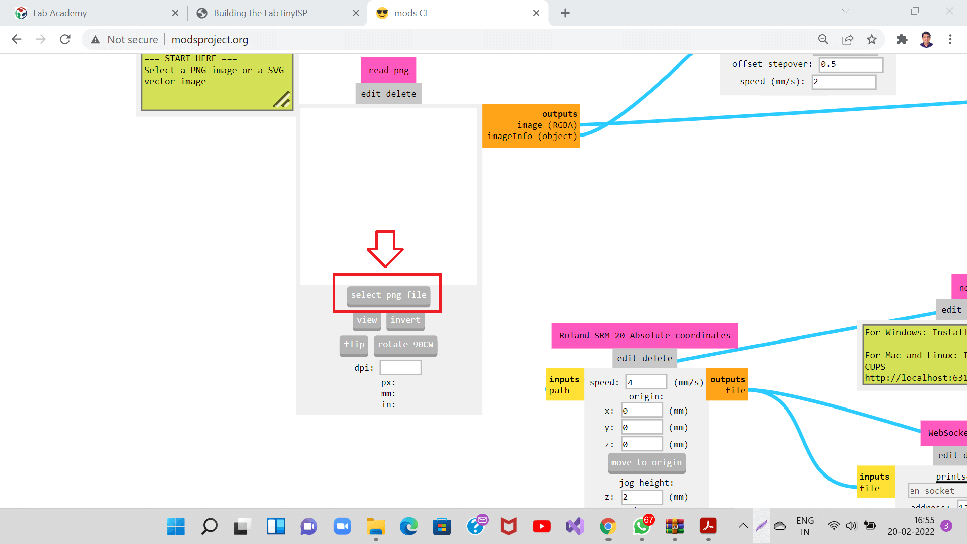
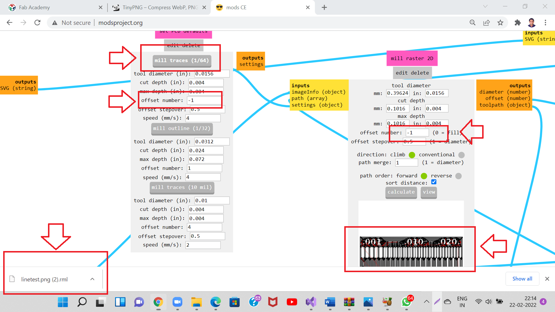
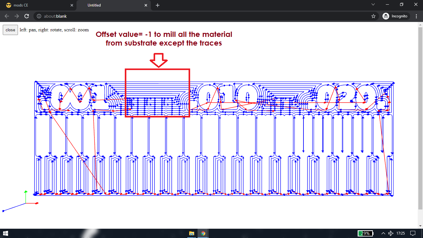
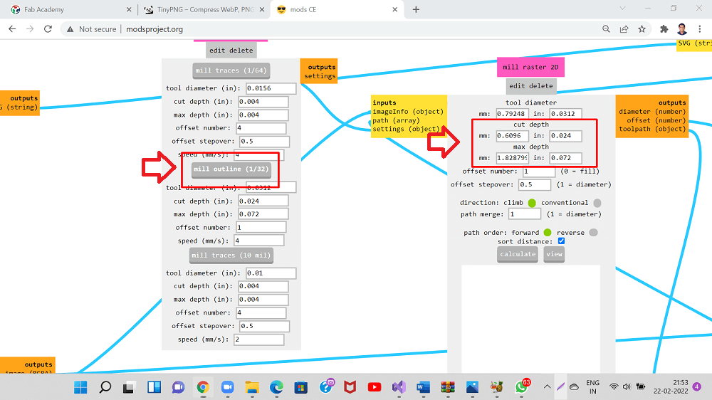
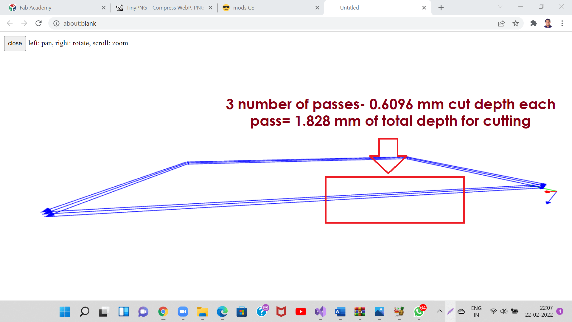
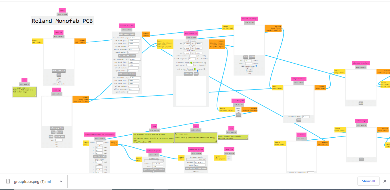
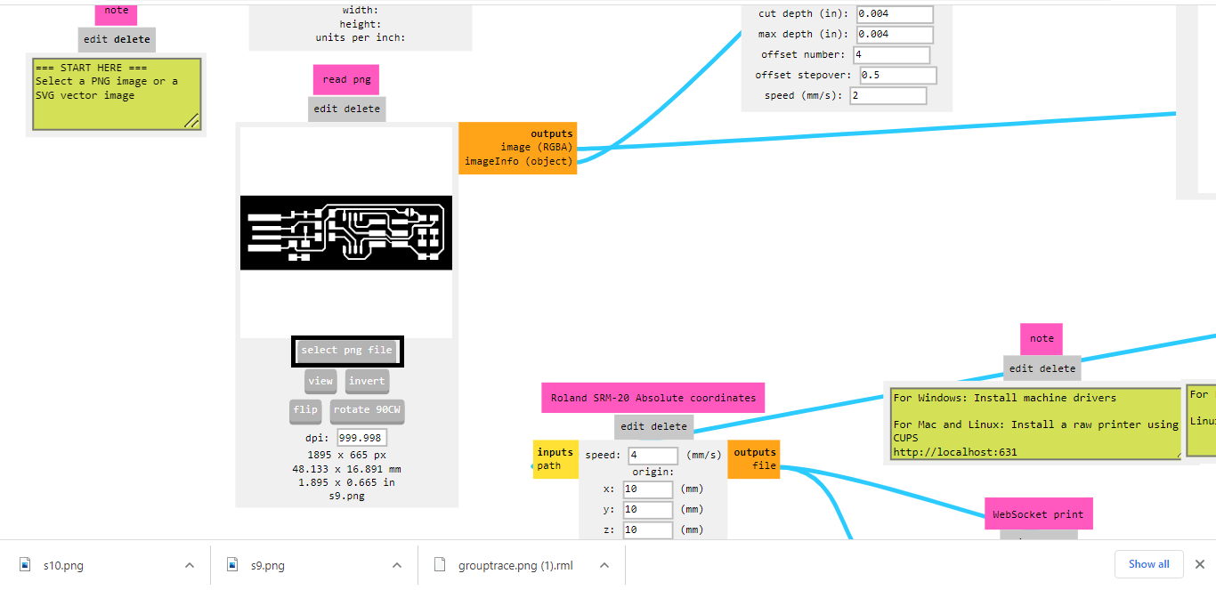
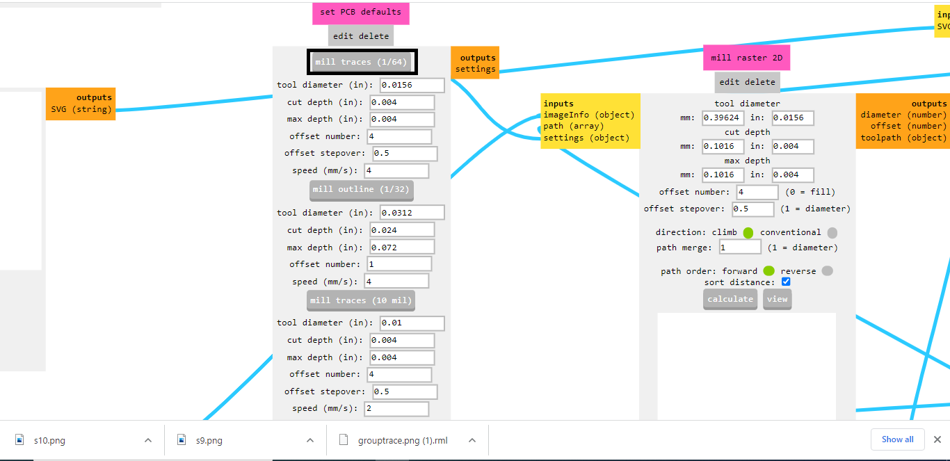
Generate the tool path for tracing and cutting:

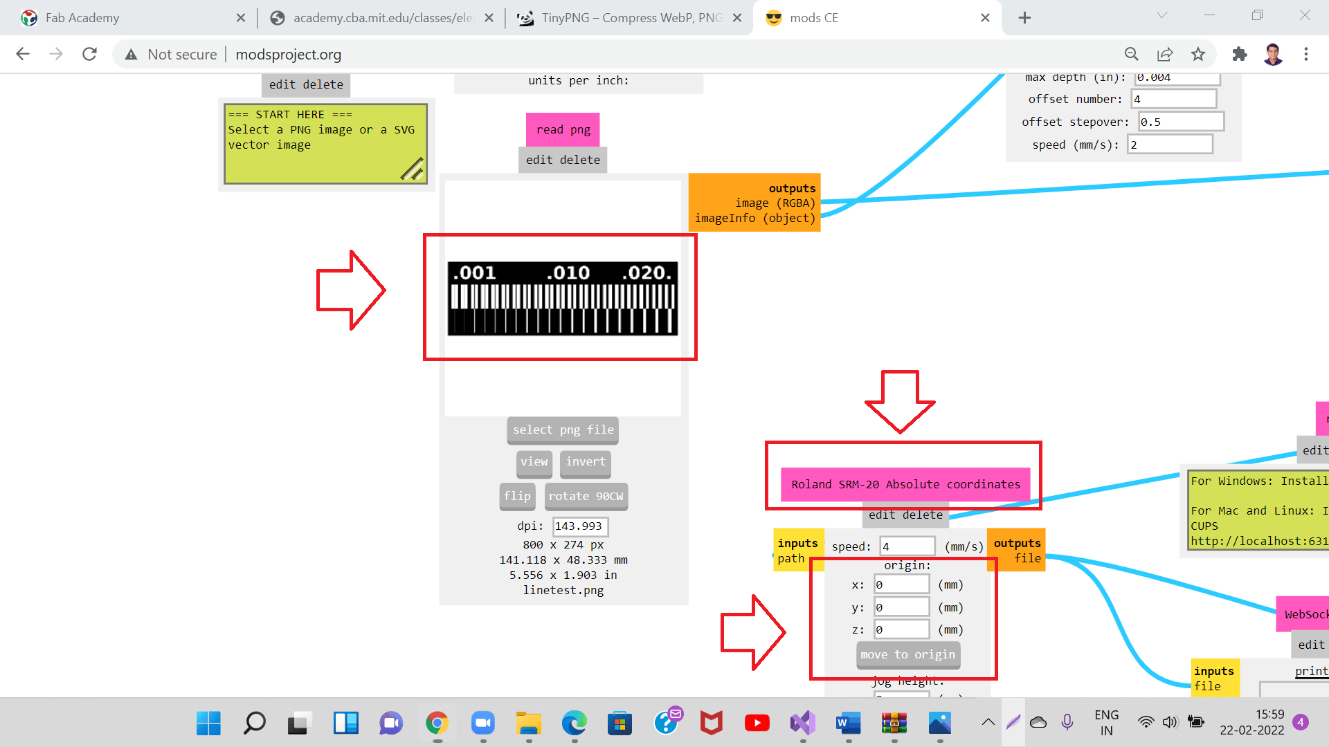
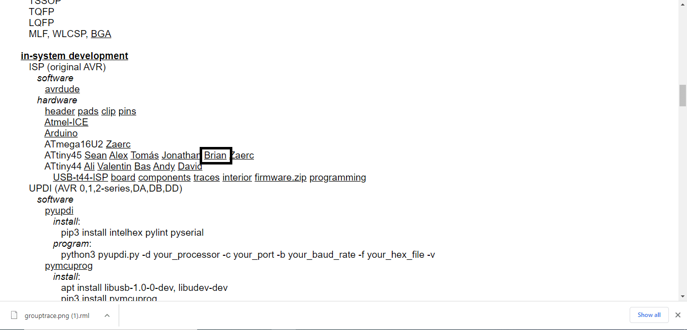
Files from Brian:-

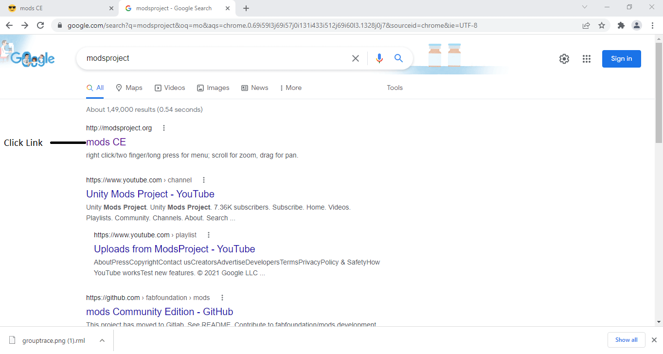
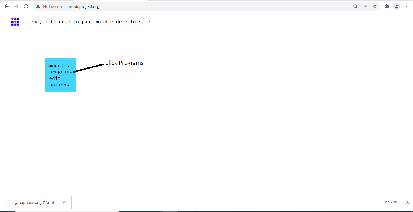
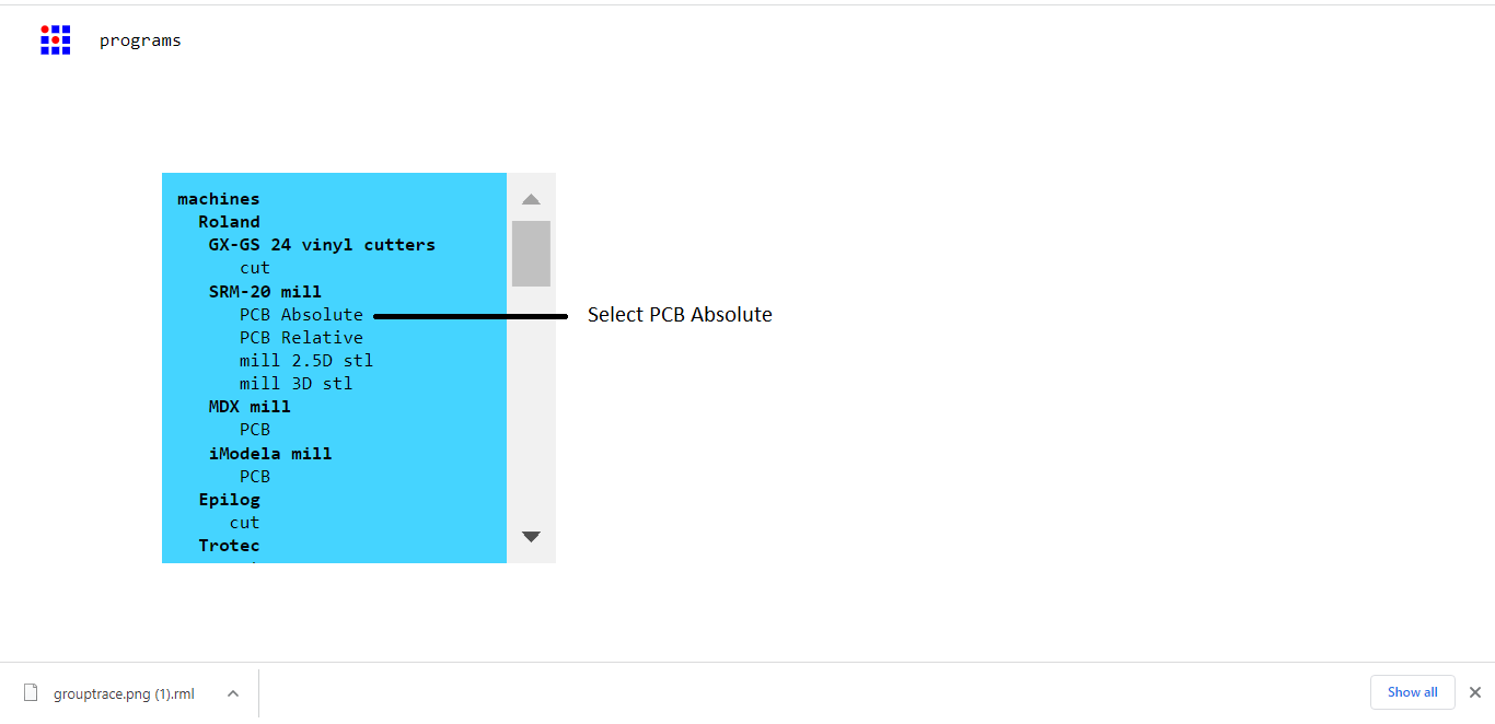
Fab modules:-


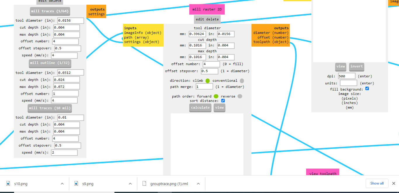

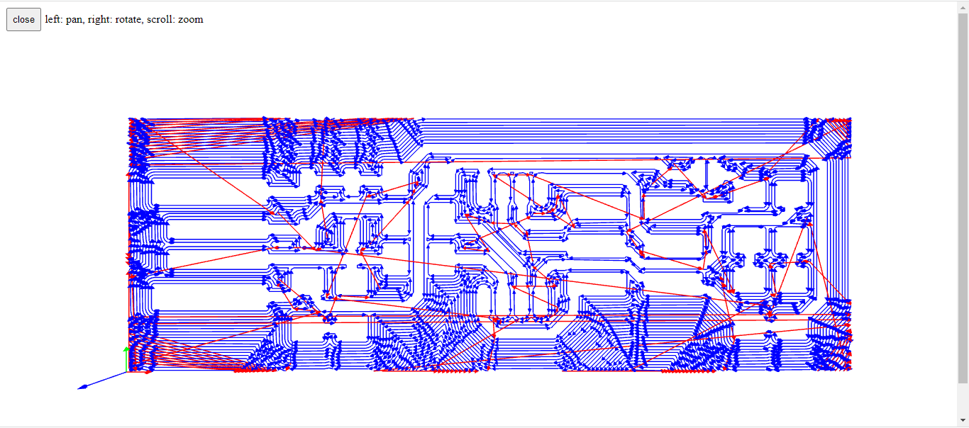
Download .rml file
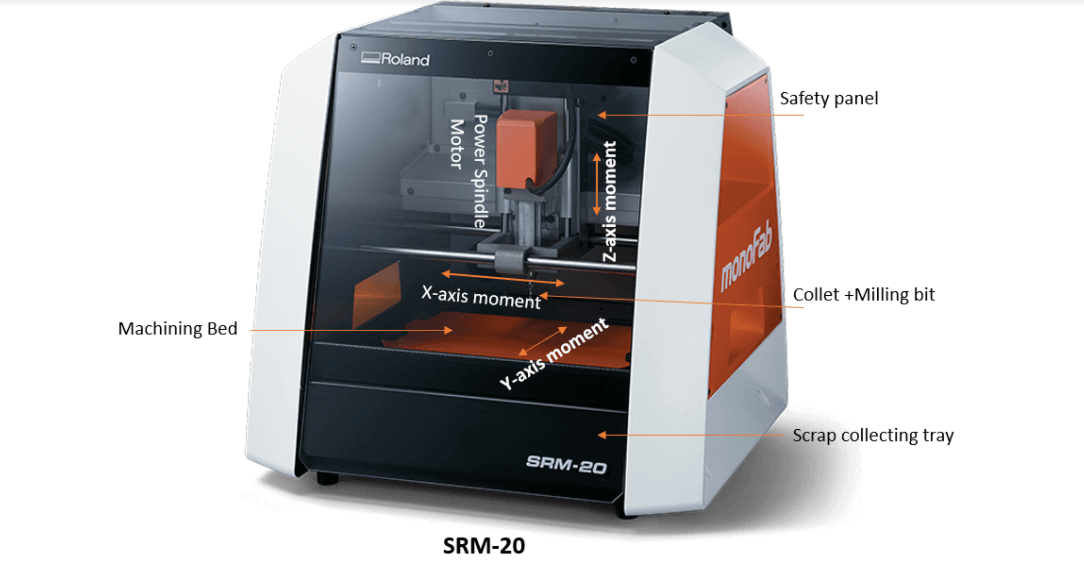
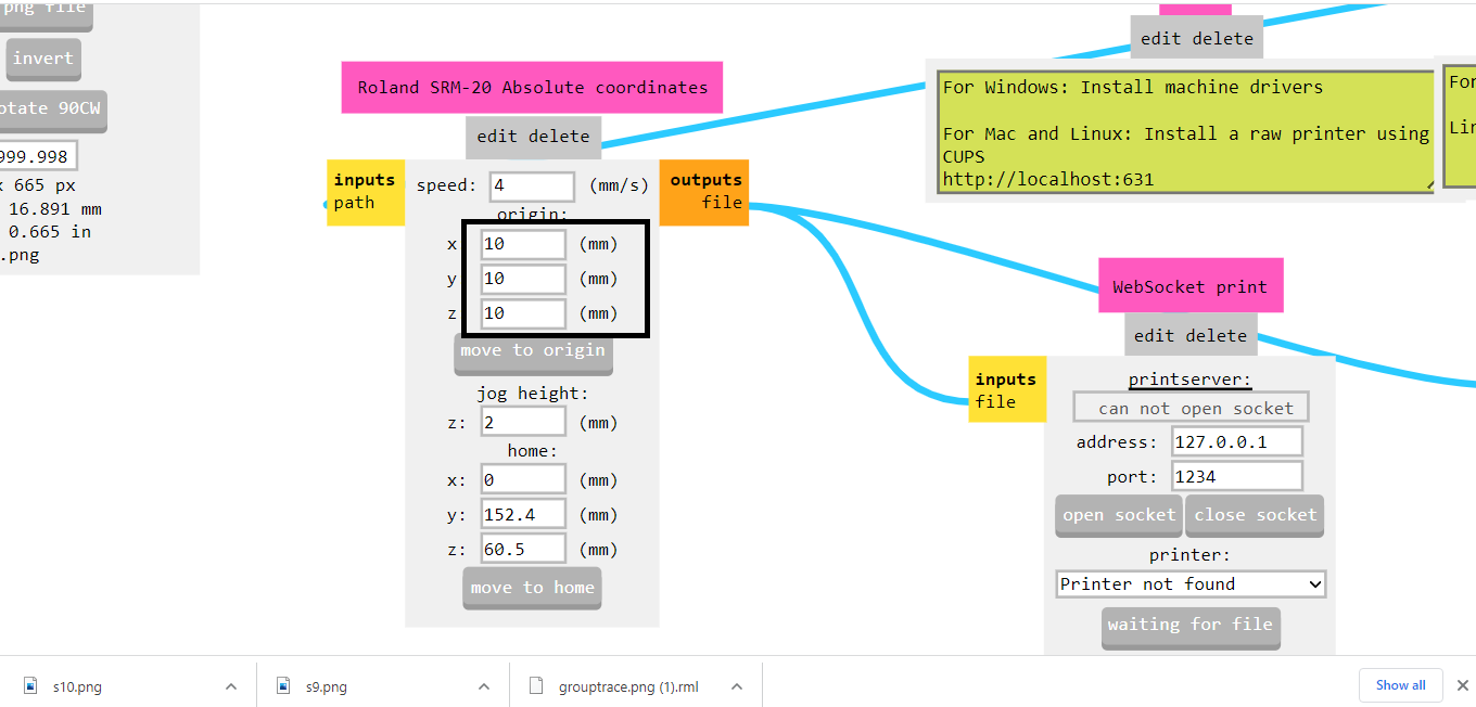
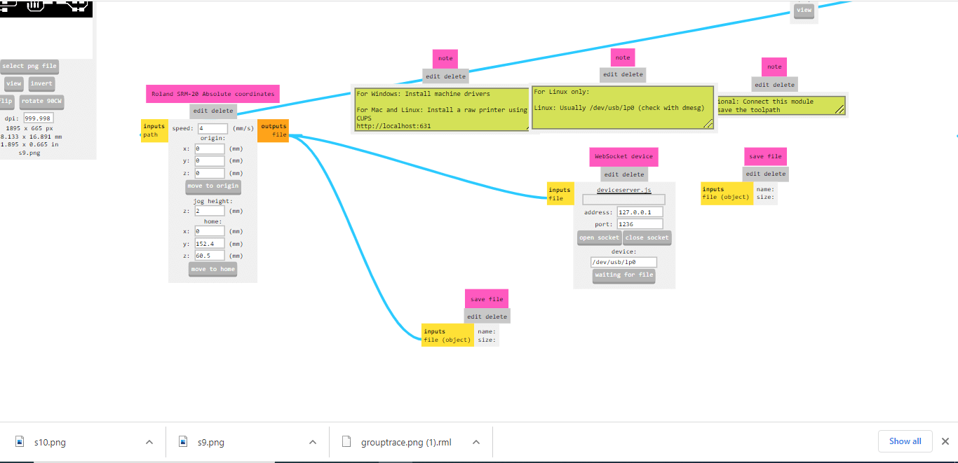
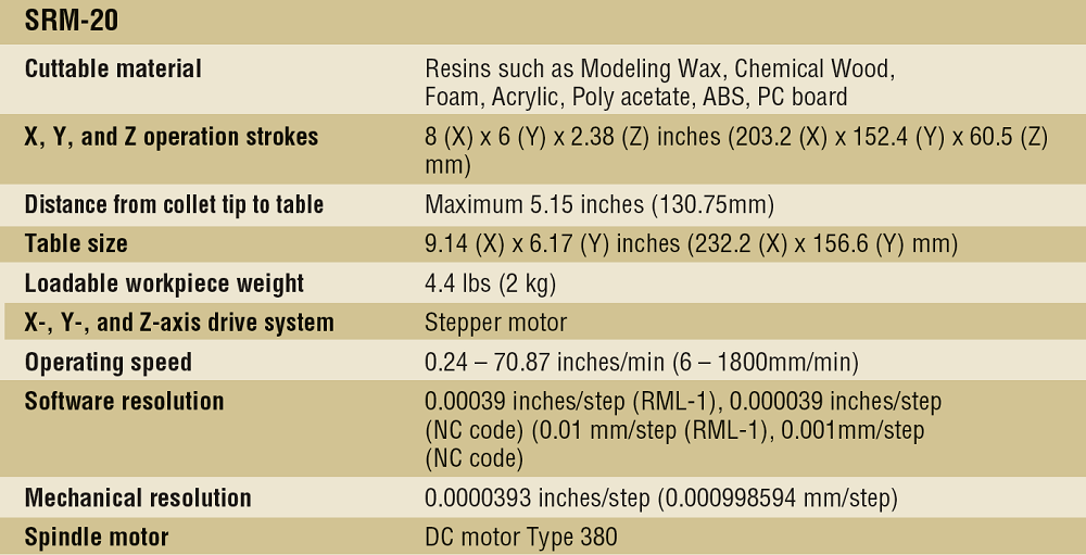
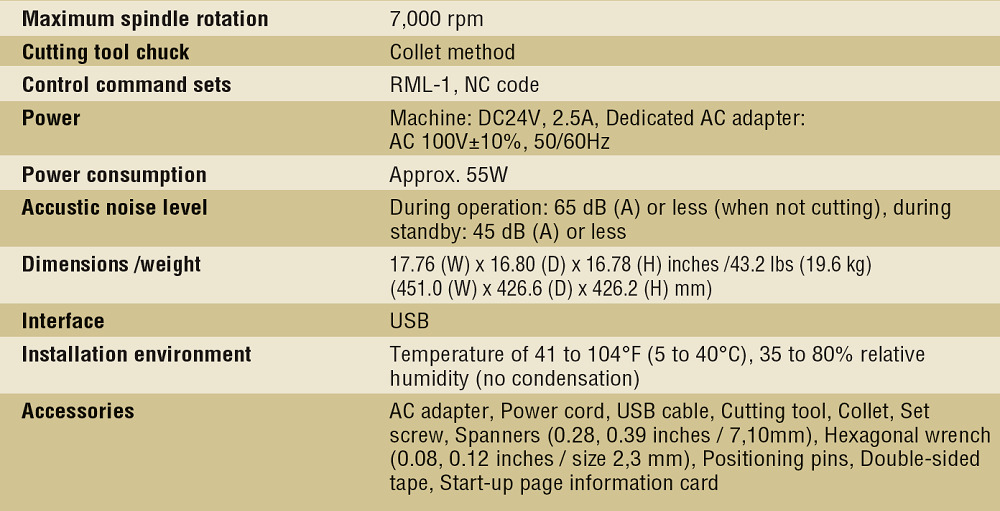
Specifications and system requirements of SRM-20
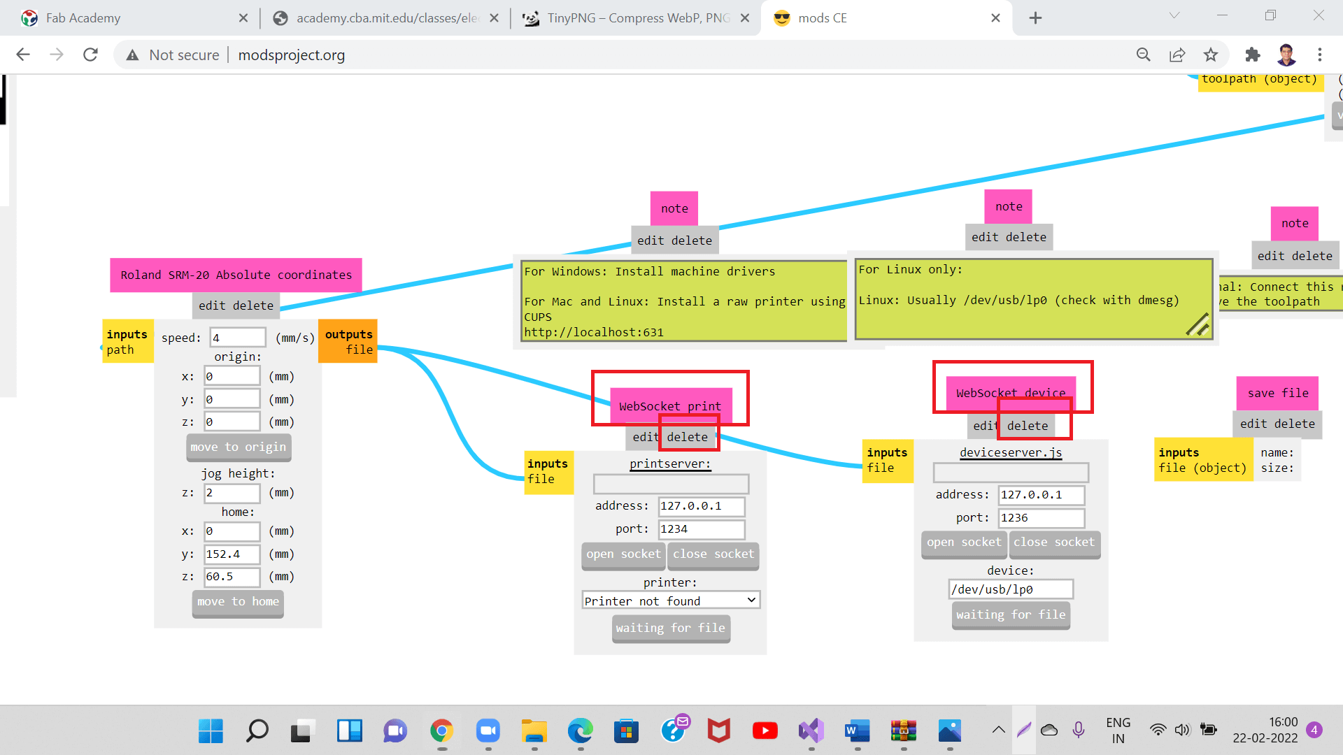
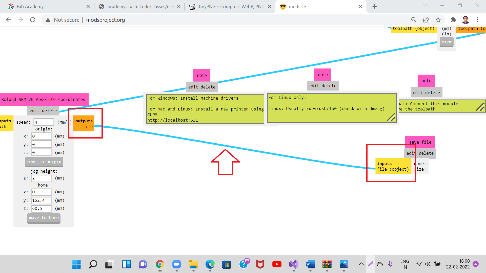
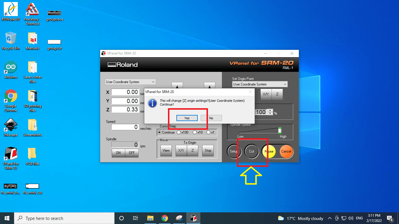
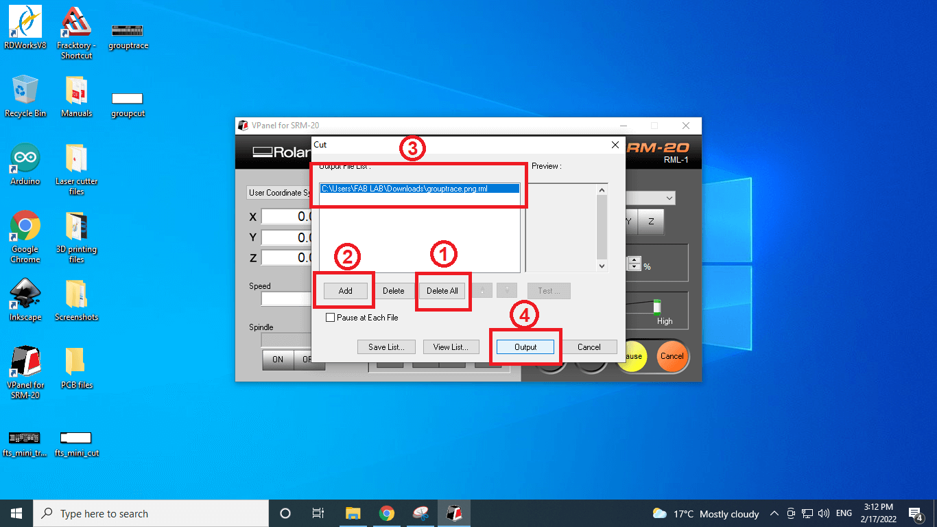
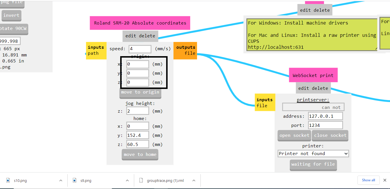
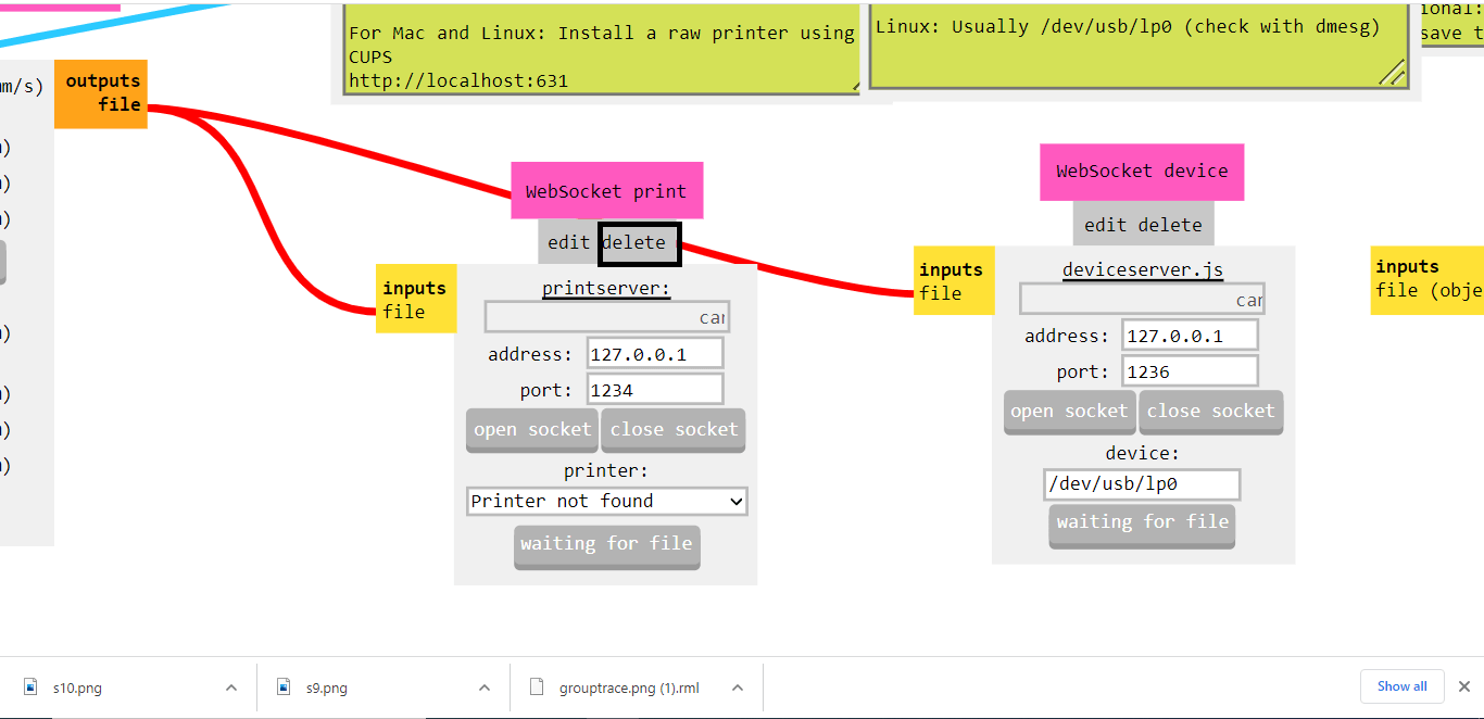
Upload File Vpanel:
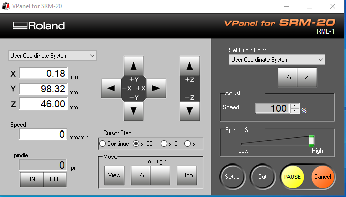
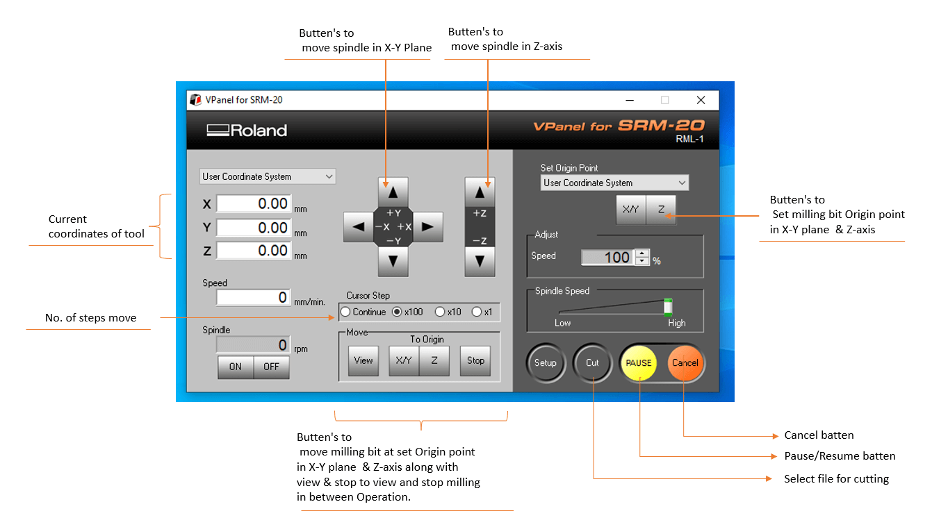
Explain VPanel
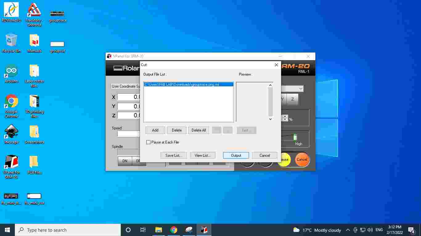
Upload Cut File VPanel
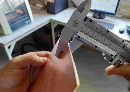
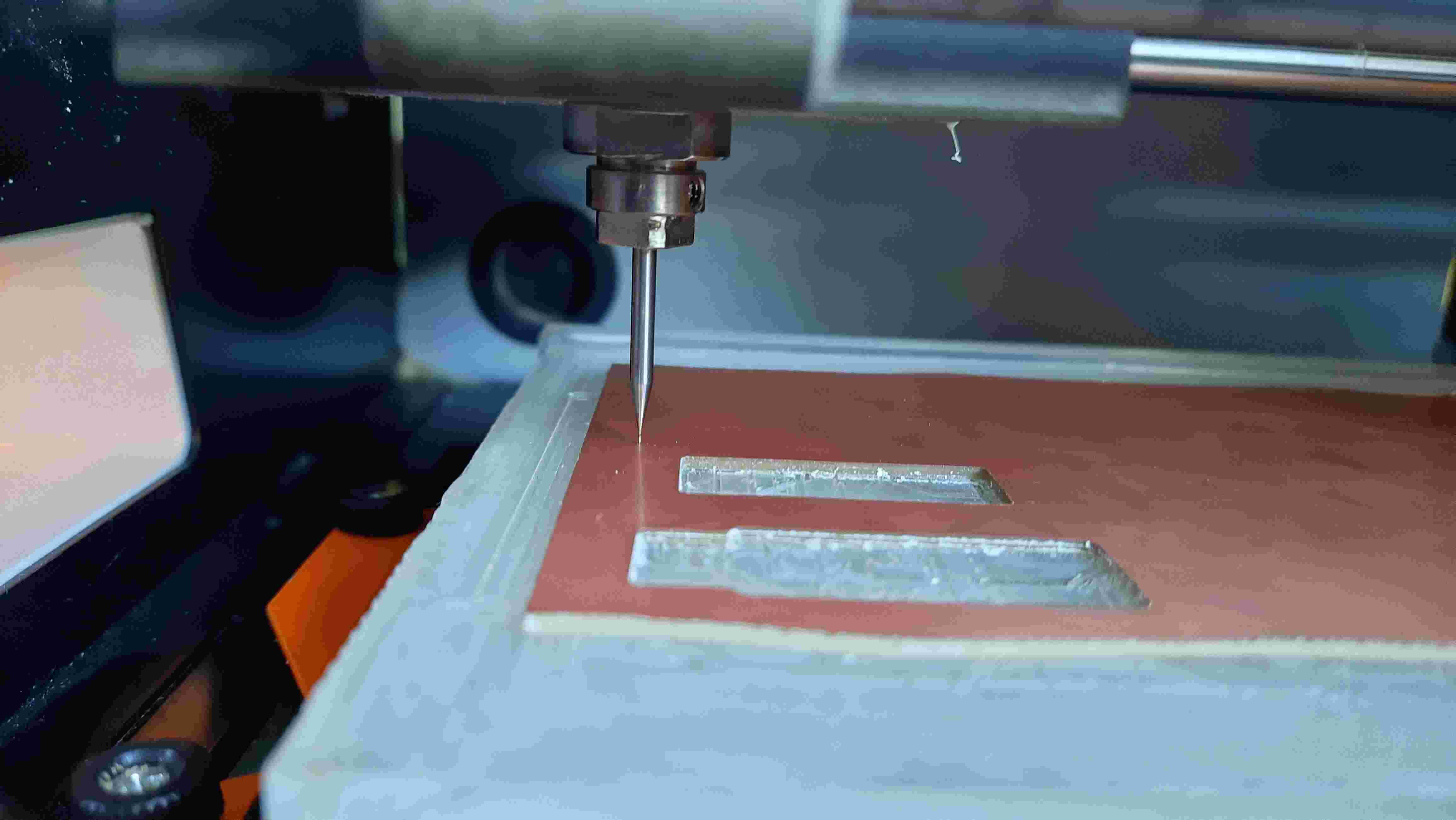
Pre-prepartion for milling
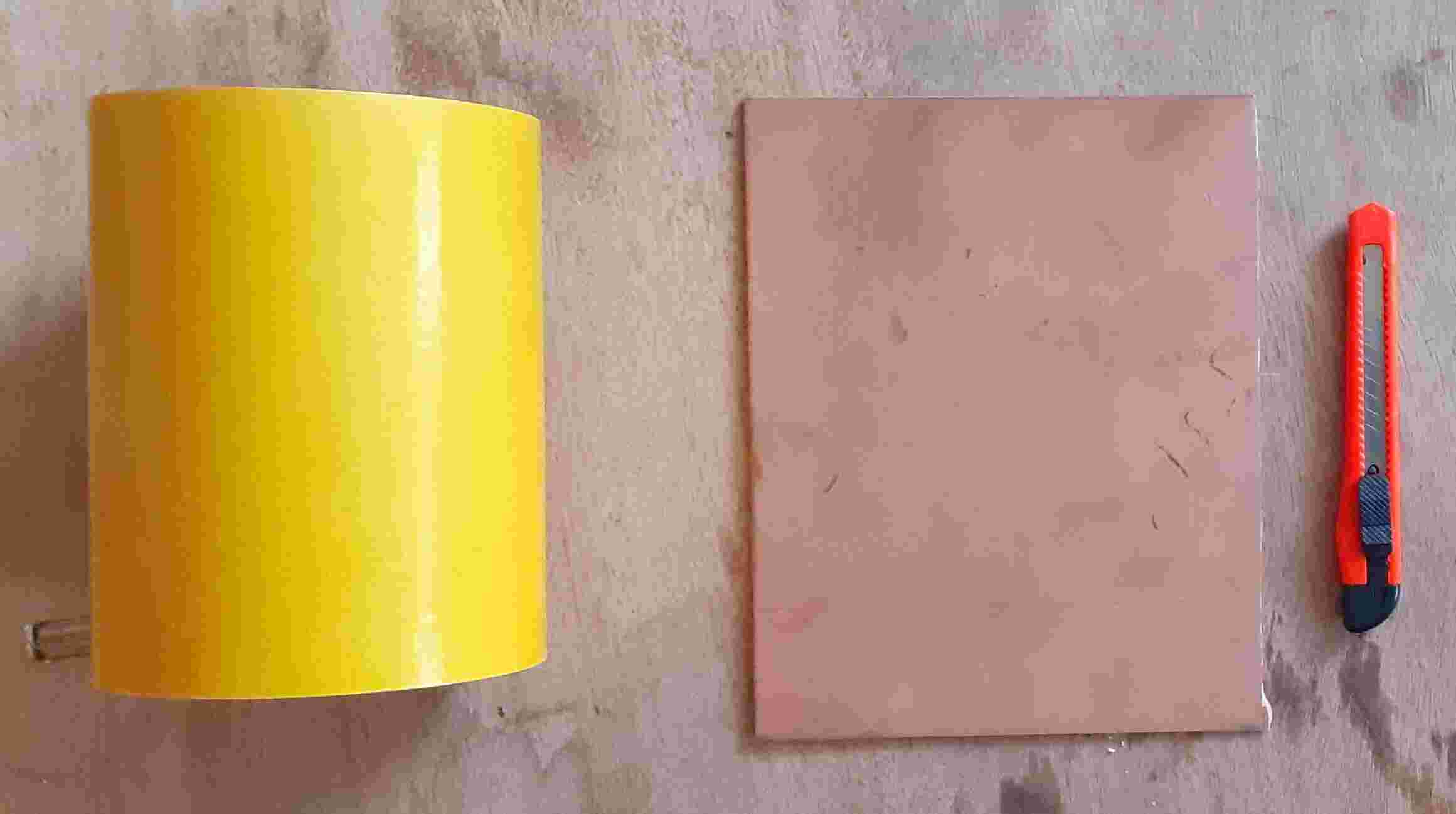
Material Thickness Check
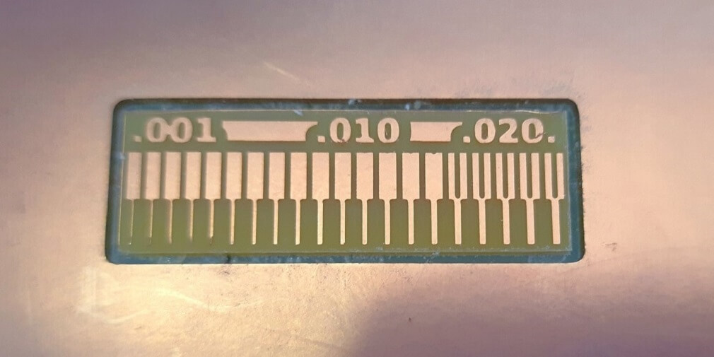
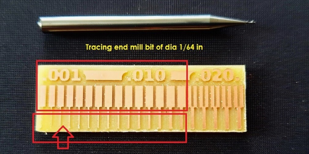
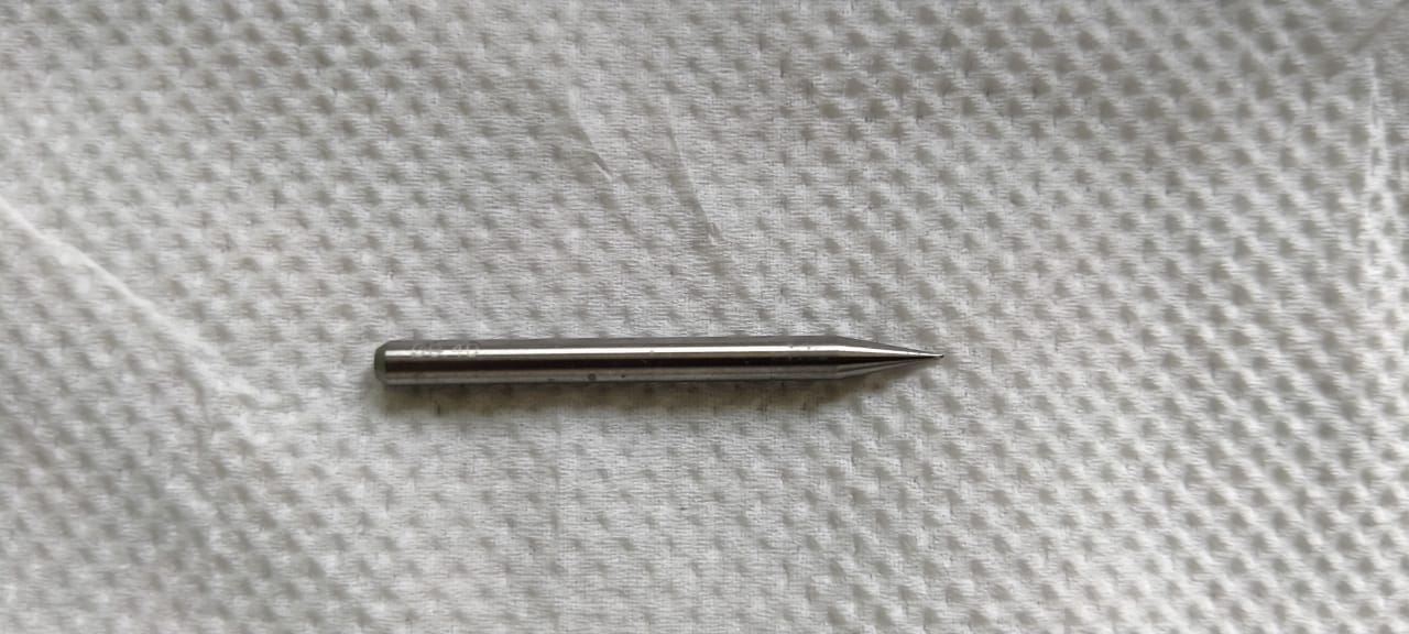
Use Bit
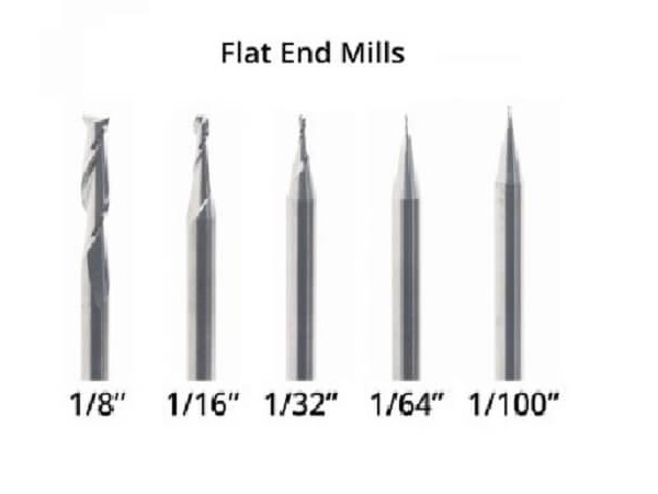
1/64
1/32
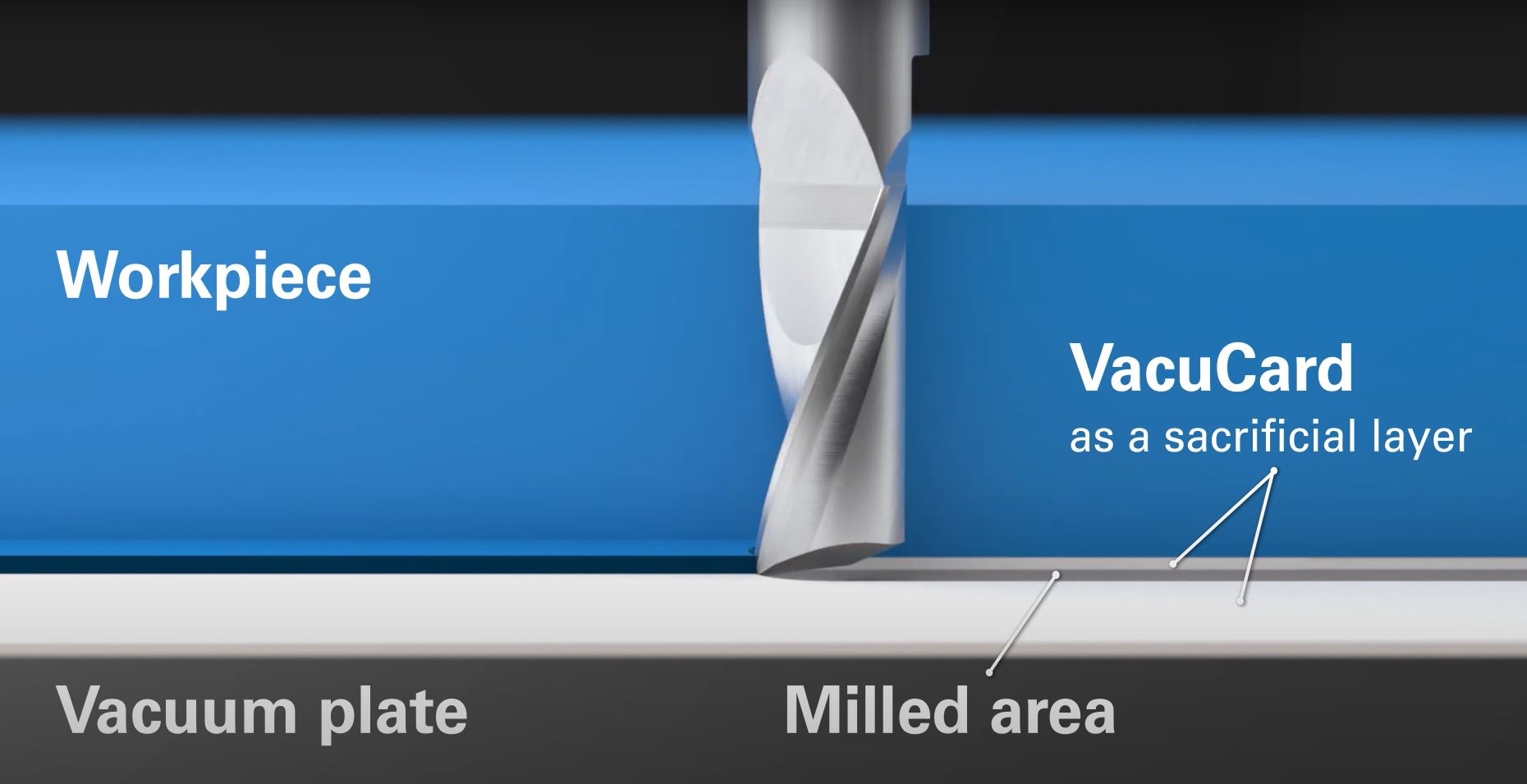
sacrificial layer
What is Solder?
Filler:
Flux:
Soldering Iron Rod:
Hot Air Gun:
Exhaust Fan:
Desolder Pump:
Twisers:
Magnifying Glass:
Light lamp:
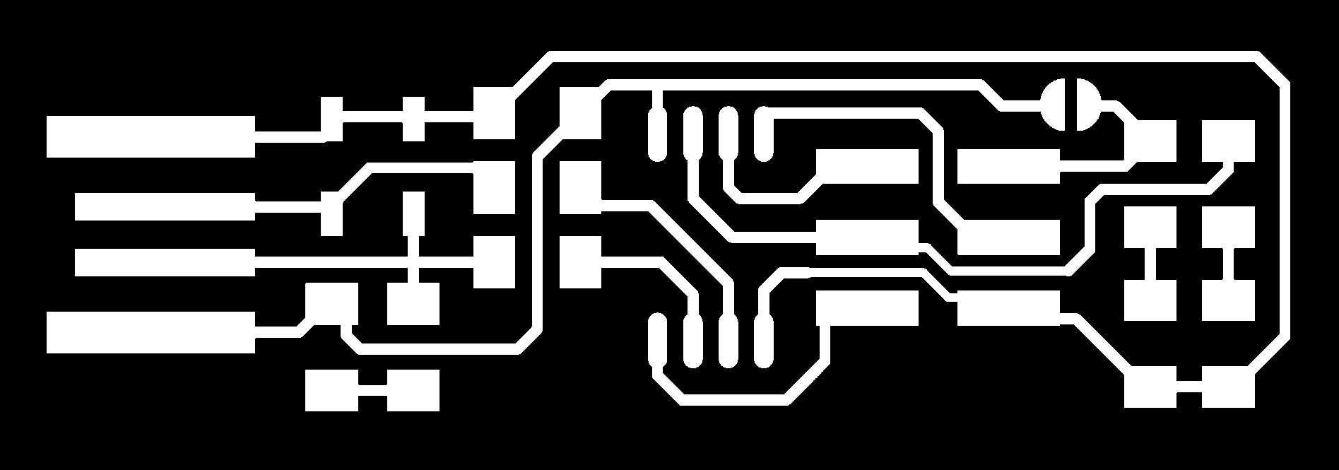
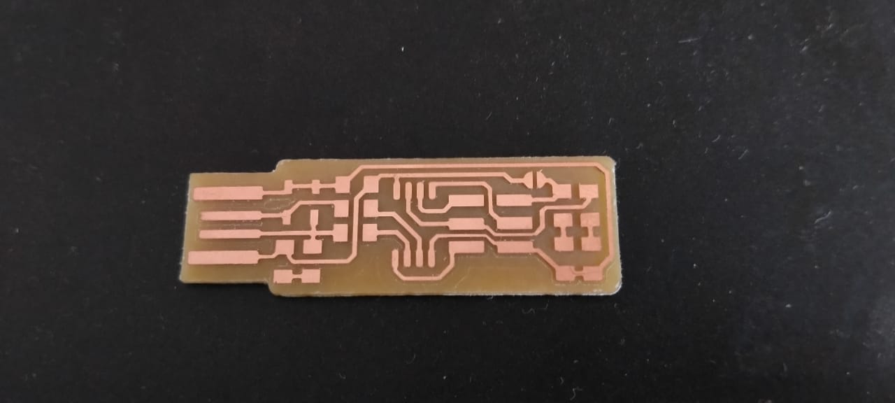
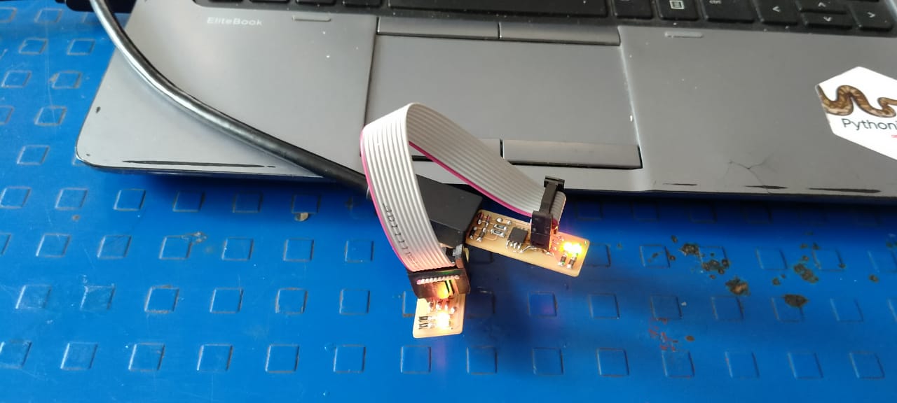
What is the FabISP?
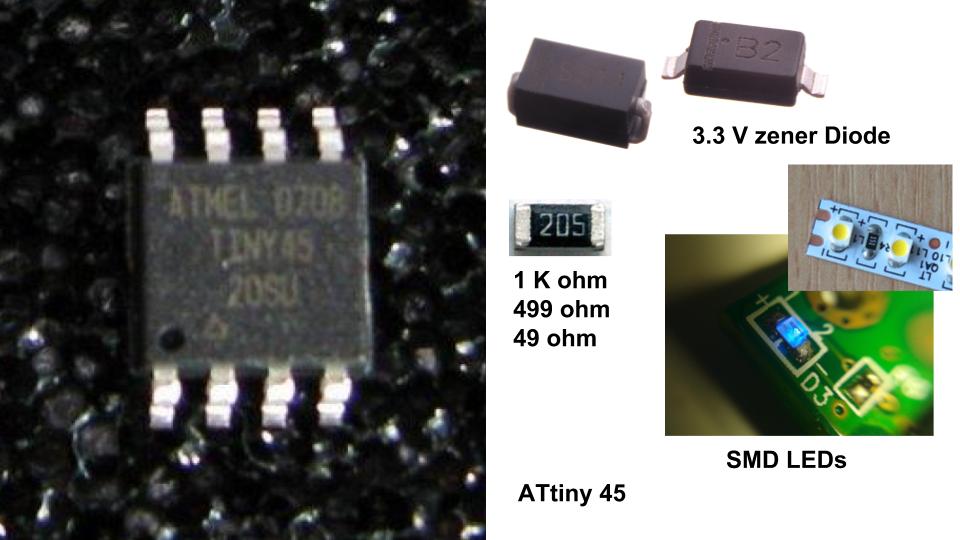
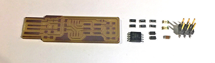
Components of circuit:
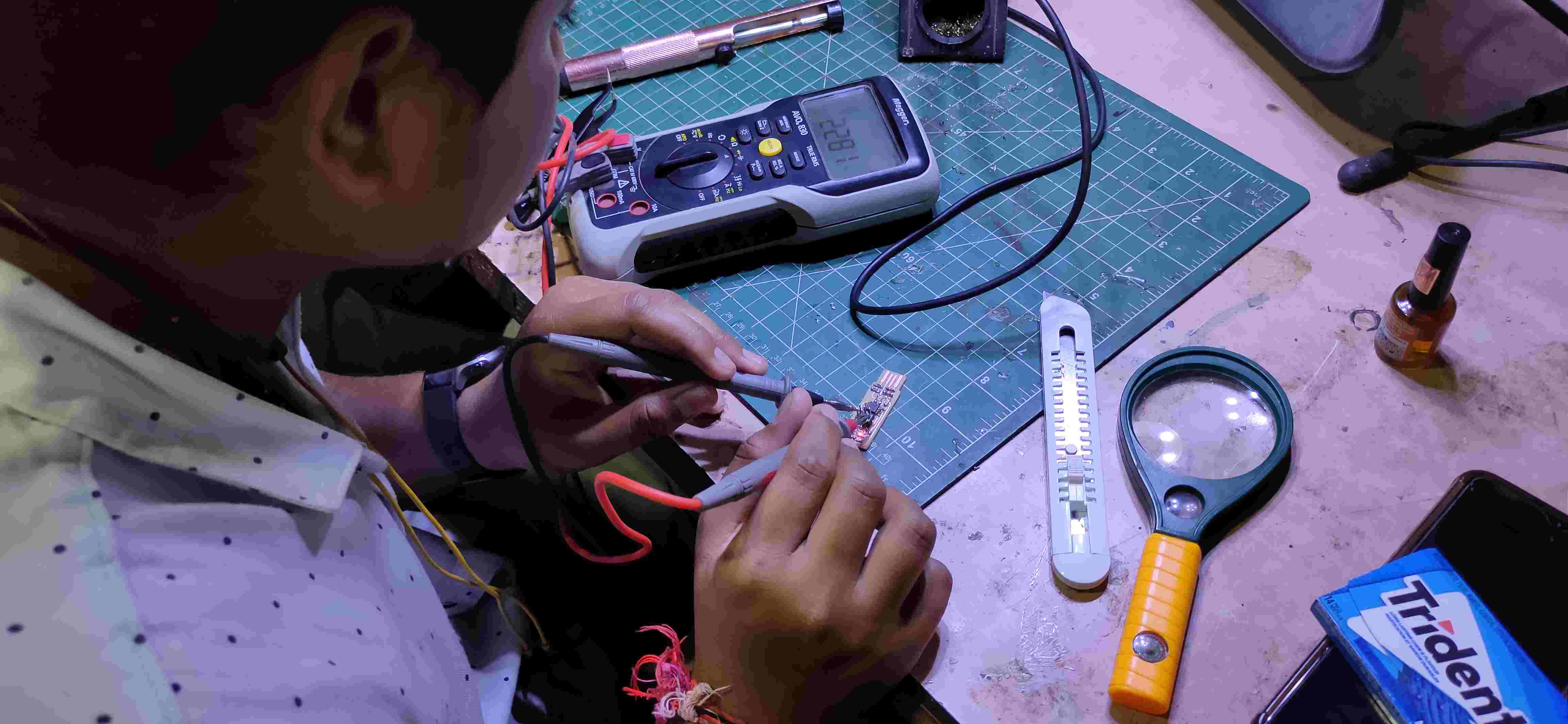
Checked Circuit
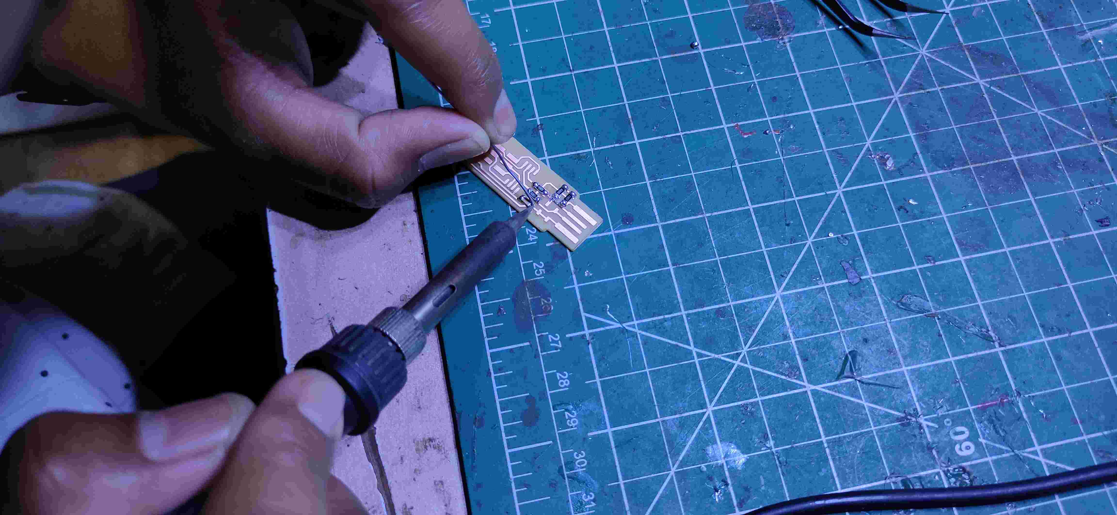
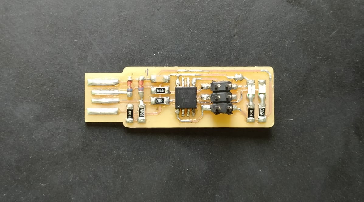
Finally Soldering Complaint
Installed GNU Make:

Updated Path:
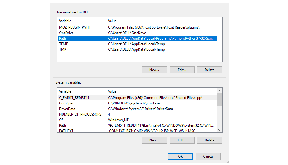
Edited Path to add the below 3 values:

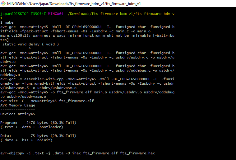
$ make
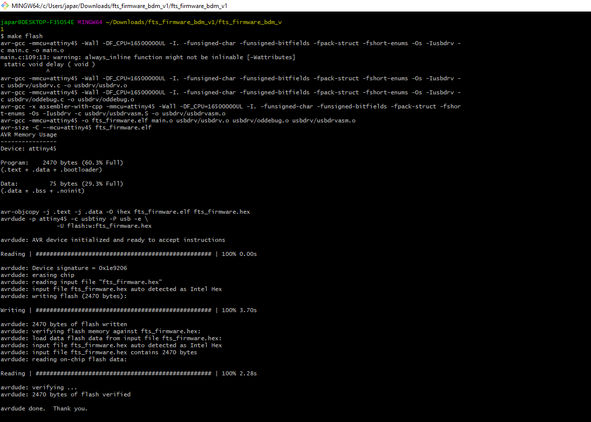
$ make flash
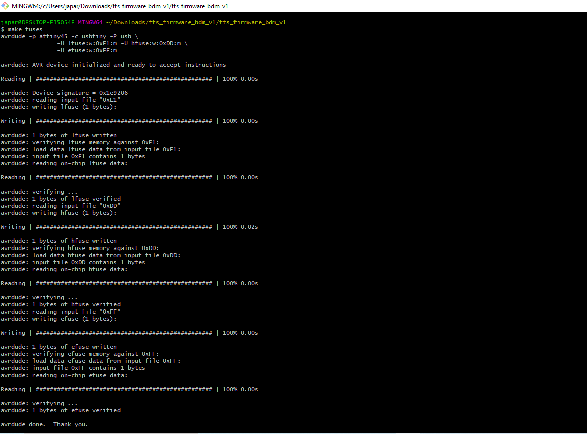
$ make fuses
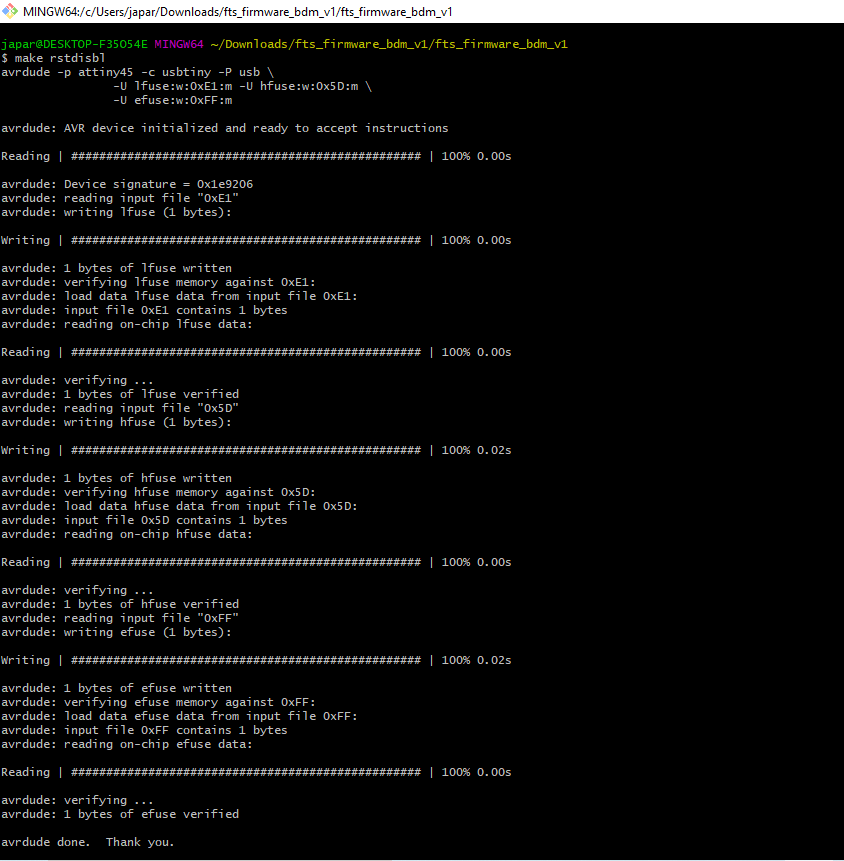
$ make rstdisbl
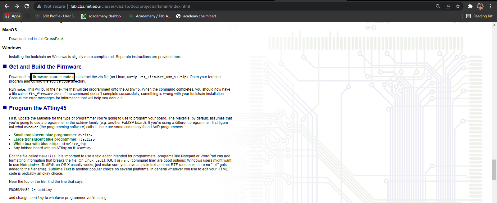
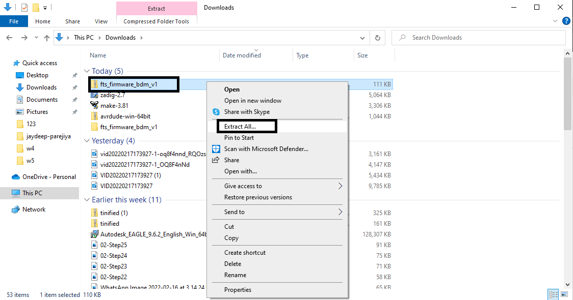
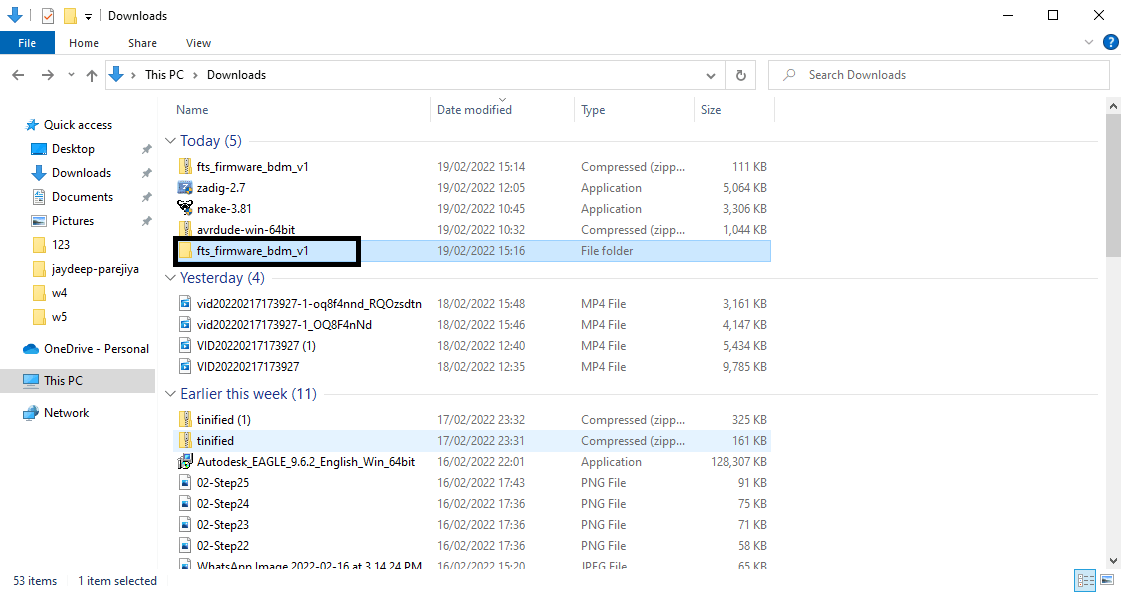
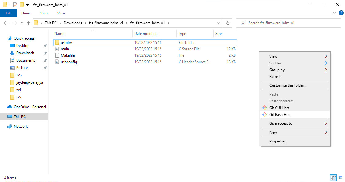
Download Source Code:
break 1/64 end mill
Refernces Link
Buildling the FabTinyISP by BrianGNU AVR ToolChain on Windows 10
Atmel ToolChain Download
« Computer Controlled Cutting | Week 04 3D Scanning and Printing | Week 06 »
Safety Switch by Parejiya Jaydeep is licensed under CC BY-ND 4.0![]()
![]()
![]()