The task list for this week:
- Group assignment:
- Characterize the design rules for your in-house PCB production process: document feeds, speeds, plunge rate, depth of cut (traces and outline) and tooling.
- document your work (in a group or individually)
- Document your work to the group work page and reflect on your individual page what you learned
- Individual assignments.
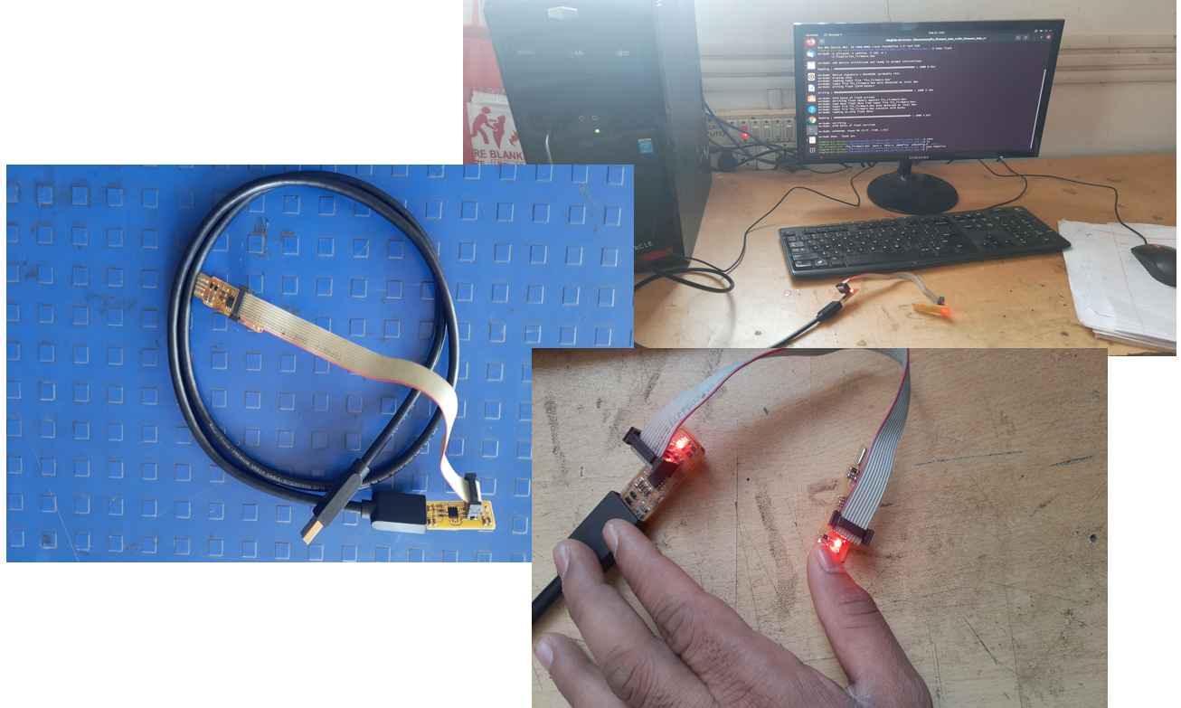
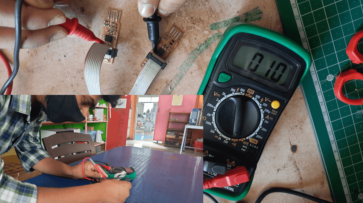
- Make an in-circuit programmer that includes a microcontroller by milling and stuffing the PCB, test it to verify that it works.
Group assignment:
Precision Test:
This week we work on PCB fabrication. we have been making our hands 1st time on the milling machines and learning to fabricate PCBs. for which we use SRM-20 a Precision and Productivity 3- axis milling machine used for doing many milling operations. In the assignment, we work on checking the precision test for our milling machine . electronic production > (CAM) section > trace width .
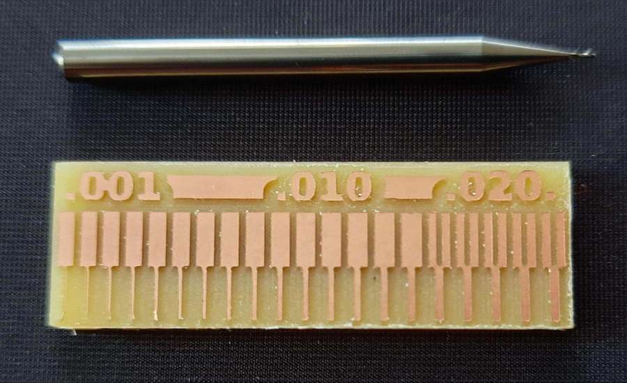
Precision test for SRM-20.
Using these results we characterize the design rules for our PCB production process.
Check here to read more about our group assigment.Individual assignments:
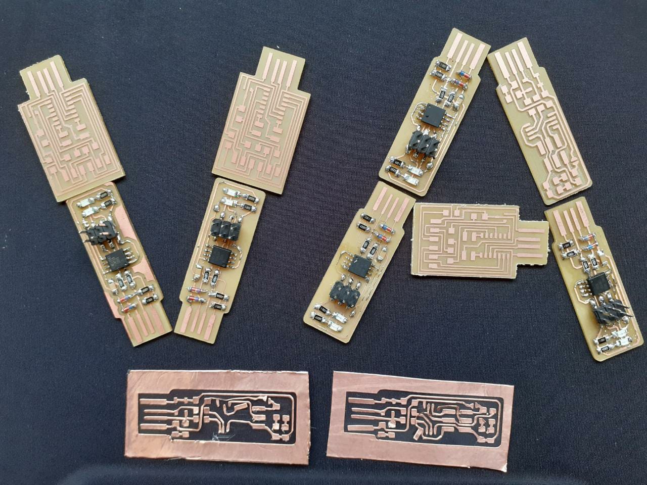
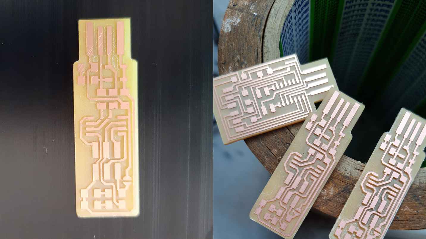
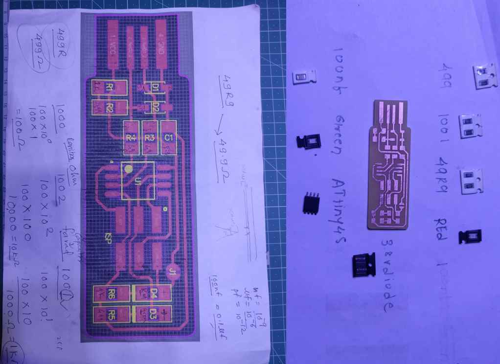
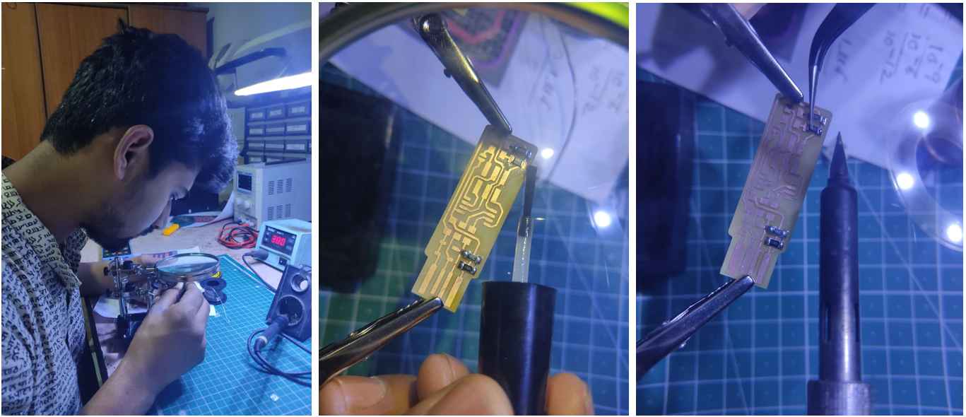
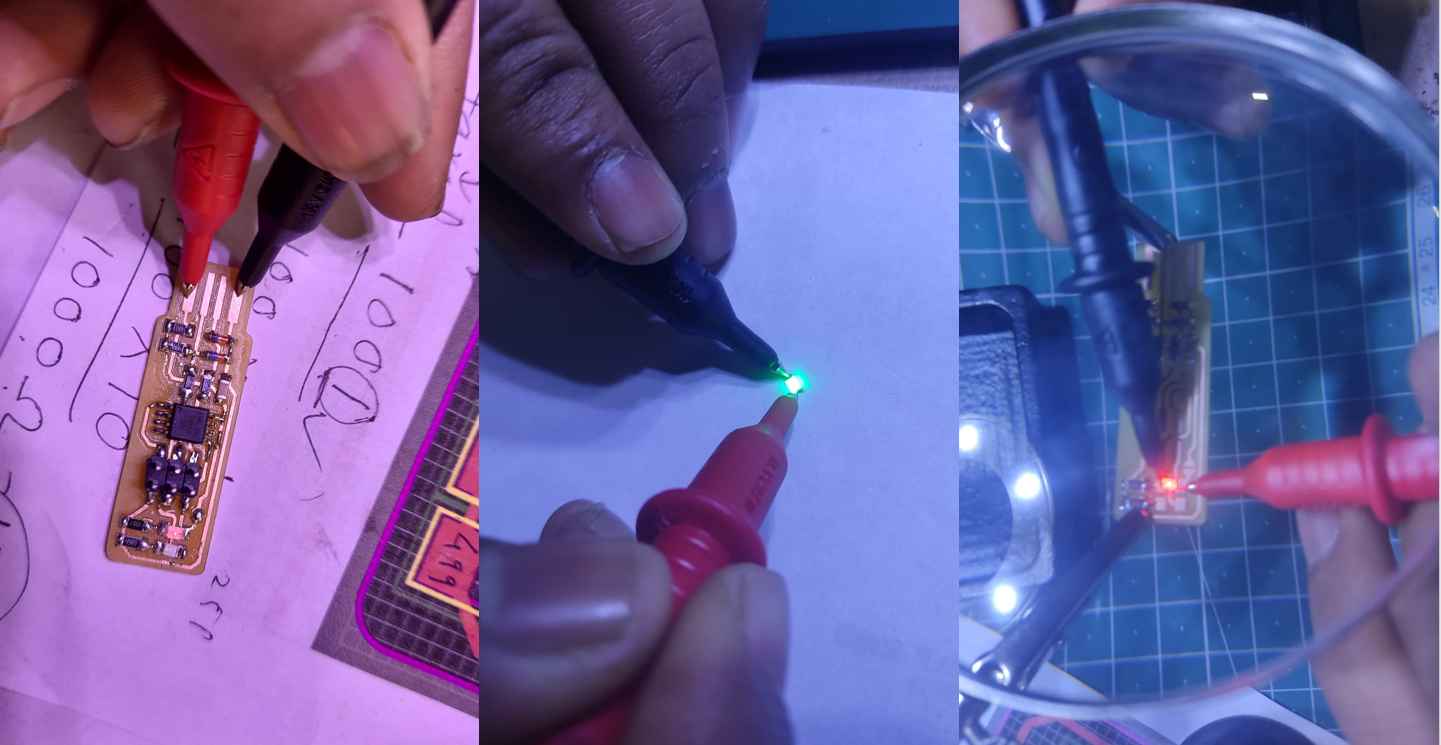
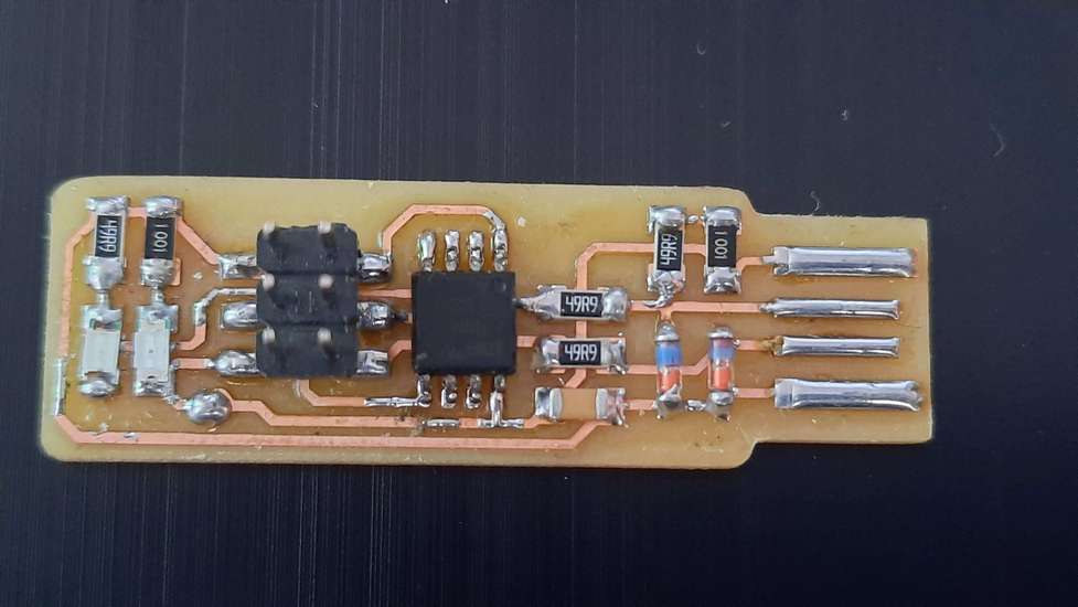
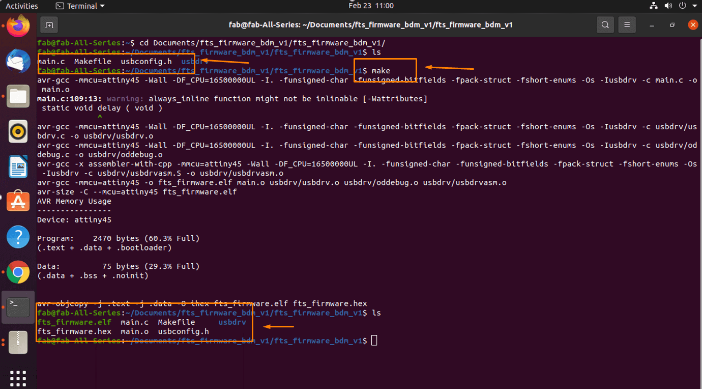
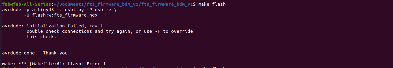
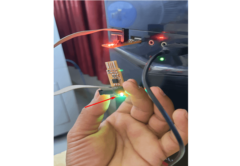
So for this week, I have to make an in-circuit programmer board. Using a microcontroller and machining the PCB board and last testing it to verify that it works.
Introduce to the programming board:
There are 4 types of programming boards I found in the fab academy.
- ISP(In-System Programmer)
- UPDI(Unified Program and Debug Interface)
- FPDI(Future Technology Devices International Limited )
- JTAG( Joint (European) Test Access Group )
Out of which I decided to make ISP for my assignment this week.I followed the blog by Brian (Building the FabTinyISP) for reference
Building the FabTinyISP :
for fabracting my FabTinyISP I use this sourae file from Brian blog
MODS for PCB´S:
I use Modes CE for creating rml file for SRM-20
For using modes I refer this
tutorial.
How I use the online MODS to make files to mill circuit boards:
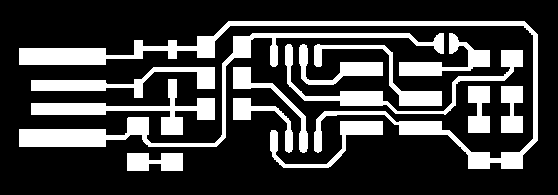
Step 1: obtain the files: Find or Design a Circuit Board
Modes program use PNG or SVG images files for generating rml file .Export/save board design as .png, You should have two or three images, depending on your PCB:
- Traces
- holes drill
- outline
For fabracting my FabTinyISP I use this sourae file directly from Brian blog.
others FabIsp option can be found here.
Step 2: MODS - Setup for PCB milling.
MODS is the new FABMODULES it more capable and works by connecting nodes to develop each process. one can customize his own workflows by loading different modules or use an already precompiled program. In my case I am going to use a precompiled program and add a module to save automatically in my computer instead of connecting directly to the machine.
- Open mods in browser recommended firefox/chrome i personaly use crome .
- Right click anywhere and select select PROGRAMS --> OPEN PROGRAM --> Roland --> SRM-20 mill--> PCB Absulute. (choose the machine you will use In my case it is SRM-20 mill)
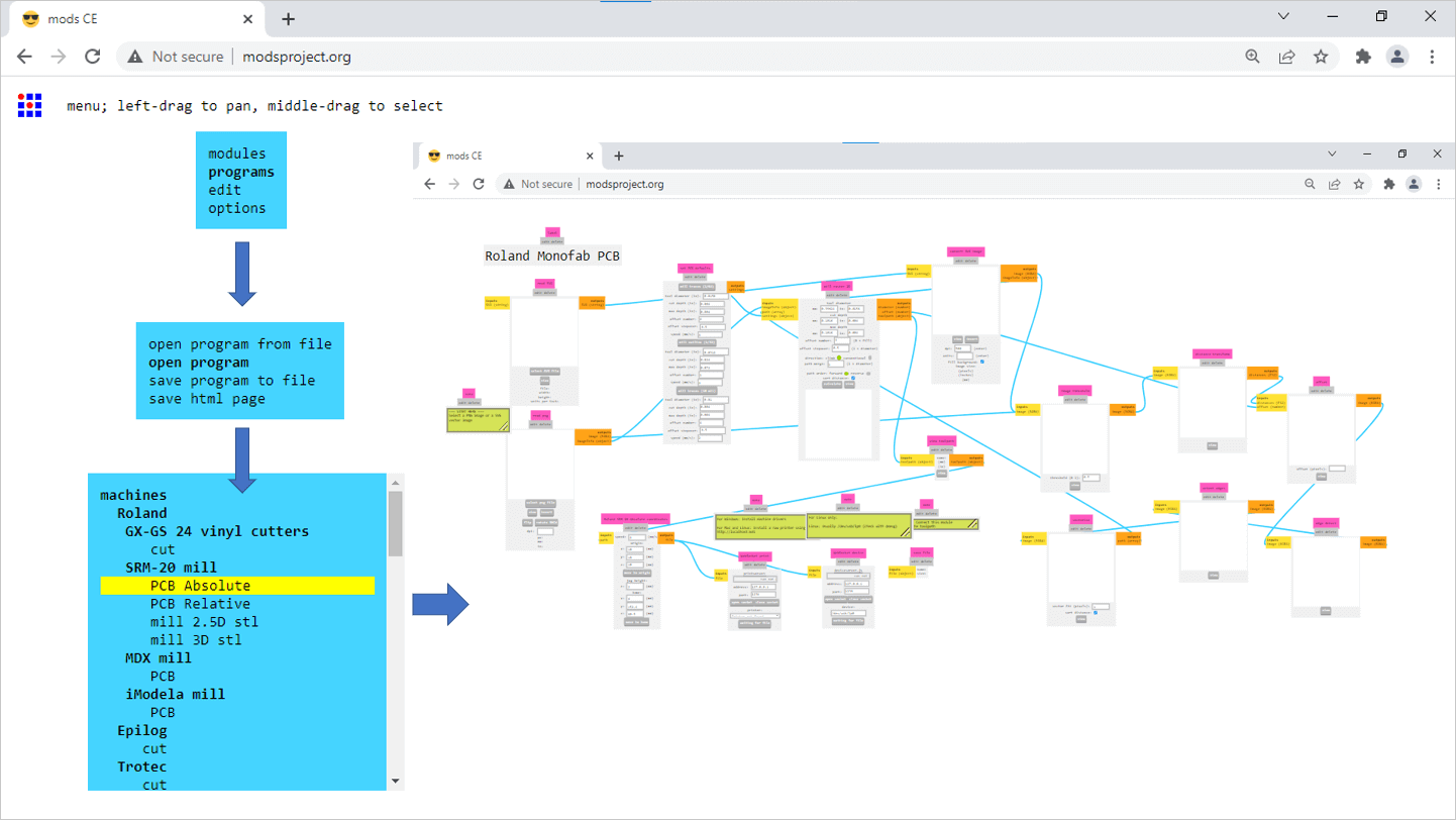
for saving rml file I need to add another module to make it save the file automatically. So we need to look for the program/component that outputs the file. In this case Roland SRM-20 milling machine and disconnect it with the out put device i did it dy deliting WebSocat Print module in program.
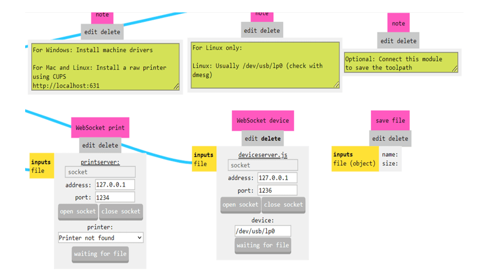
Right click anywhere in the white space and select MODULE > OPEN MODULE > FILE( > SAVE)
Now connect the elements by clicking on OUTPUT of RolandSrm-20milling machine and clicking again in INPUT of save file module to make the connection/ wiring between them.
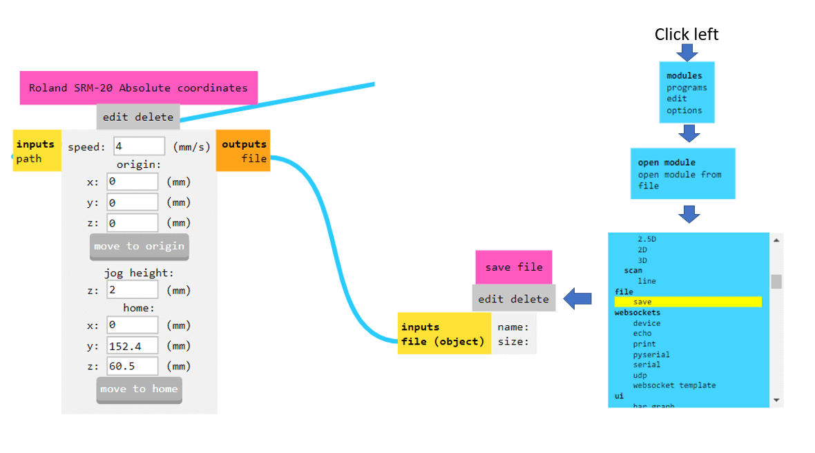
Values that I Modify
Origin Roland SRM-20 milling machine in module.
- x0(mm) - 0
- y0(mm) - 0
- z0(mm) - 0
- zjopg - 2
x/y/x home is the parking position after finishing the cut
I set other things as defalt they are in program.
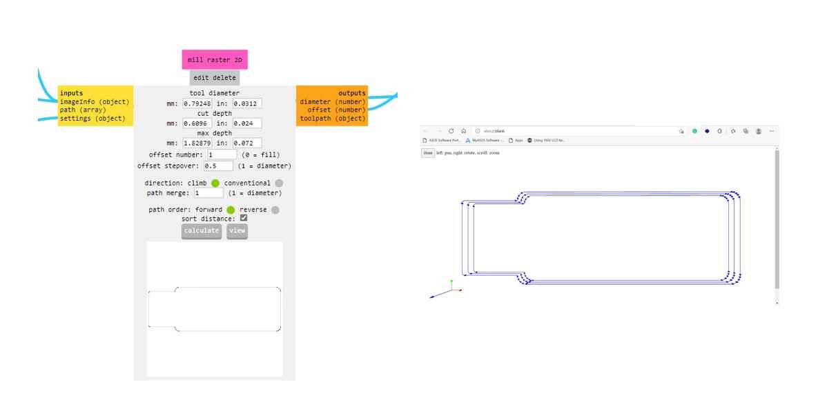
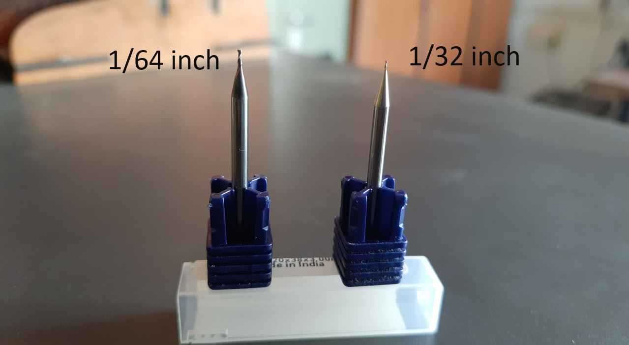
Step 3: MODS - Setup for Traces (1/64):
Open traces image file in program (This is the one with lines that will form the wires between components.)
for that I go to READ PNG MODULE SELECT- PNG FILE - select traces image and uplode it.
then I click in MILL TRACES 1/64 in SET PCB Default module for seting program for 1/64 milling bit.
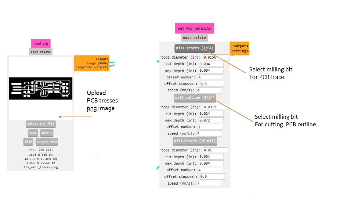
Than I Click "calculate"(you will see the path calculating), when the process finish it gets "automatically be saved into downloads folder".
The file will be saved automatically into your download folder.
Values that I Modify
- tool diameter:define dimeter of selected milling bit
- cut depth:Define feed dipth of milling bit
- max depth:Define feed dipth of milling bit
- offset number:Define no. of offect passes per traces.
- offset stepover:Define offset distance per offect with respect to tool dimeter in my case o.5 =1/2 dimeter(dimeter=1)
- direction:climb/conventional.
- path merge:climb/conventional(-1 = fill).
- path order:forward/reverse.
The file will be saved automatically into your download folder.
Step 4: MODS - Setup for Outline Cutout (1/32):
Repeat the same process again for Outline Cutout . Open Outline Cutout image file in program (This is the one with lines that will form boundry line for components.)
for that I go to READ PNG MODULE SELECT- PNG FILE - select Outline Cutout image and uplode it.
then I click in MILL TRACES 1/32 in SET PCB Default module for seting program for 1/32 milling bit.
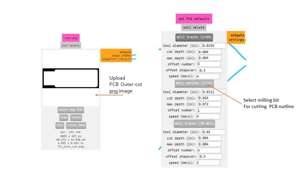
I keep all the valuse as it was in program except the origin setings which i make agent this time as prives.
Values that I Modify
Origin Roland SRM-20 milling machine in module.
- x0(mm) - 0
- y0(mm) - 0
- z0(mm) - 0
- zjopg - 2
PNG image and RML file generated.
Than I Click "calculate, to finish it and downlode the RML file in" downloads folder".
CNC Milling Machine( SRM-20):
Vigyan ashram fab-lab has a monoFab SRM-20 Desktop Milling Machine a Precision and Productivity
3- axis milling machine used for doing many milling operations. come with a software VPanel controller to regulate
feed rate, spindle speed, and milling on a complete X, Y, Z axes, and a collet system that allows for faster setting of
the Z-axis base point and quick tool changes.
To know more about SRM-20 Milling Machine chick out its
manual.
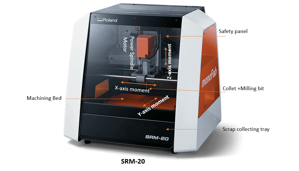
Vigyan ashram fab lab CNC milling machin.
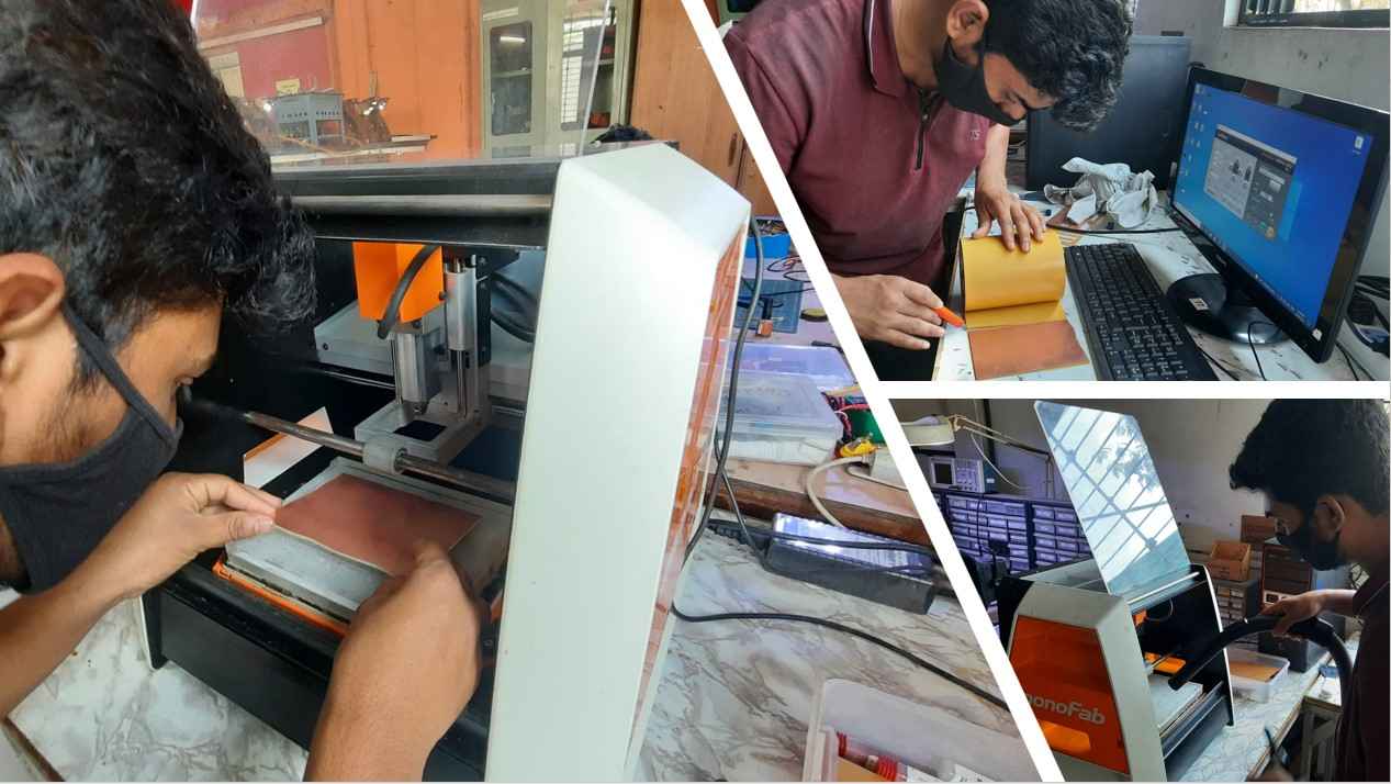
For this week of electric production, we use FR1 PCB where the insulation is made of phenolic paper for our PCBs fabrication.
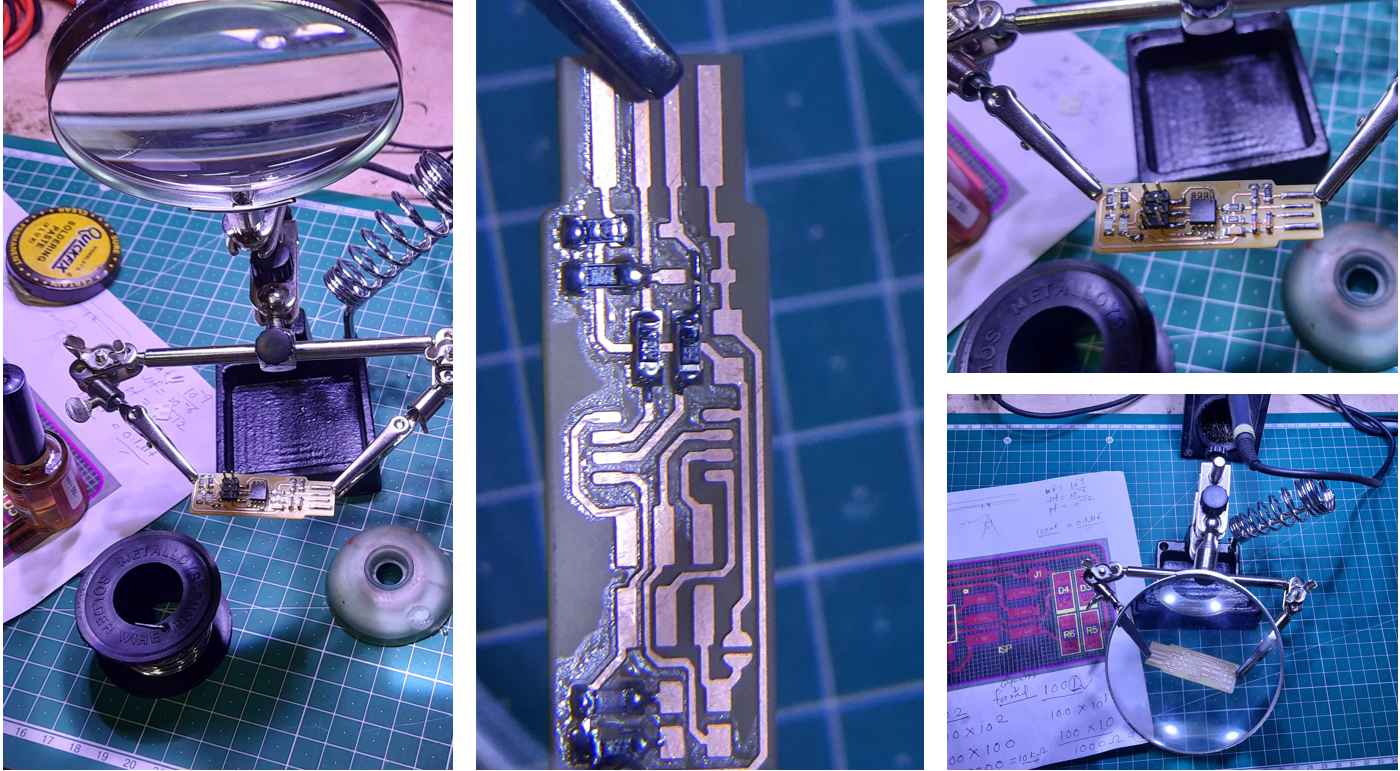
Operated the PCB milling machine( SRM-20):
Mounting PCB bord on machine bed:
`
It is good practice to 1st clean machine bed befour mounting PCB on it. I apply double sided tape all the way across (see photo) to PCB making sure it’s flat as well, with no folds, particles or overlaps under or on it. and Place it down on the sacrificial board securely on miling machine bed.
V-panel:
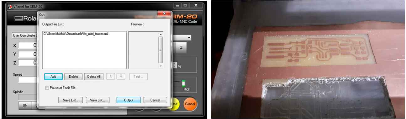
VPanel for SRM-20 is a dedicated software for controlling this machine. using this softwere one can operate this machine and make various settings using this software. .It is a CAM program use to send the rml file SRM-20 CNC.
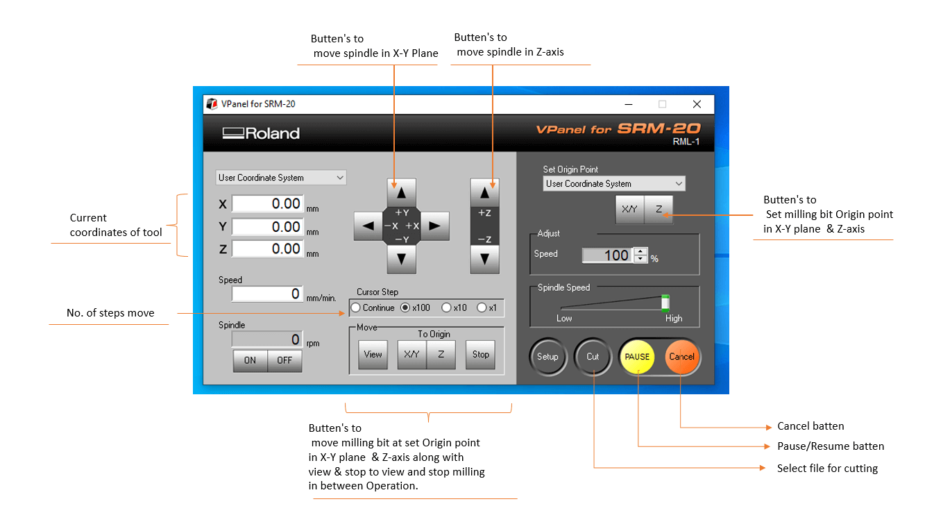
V-Panal for controlling SRM-20.
1.Setting up the cutting tool (End mill):
It is very important to set the tool in perfect way to avoid tool bracking ,wobbling of tool which can damage the PCB it self during machining as well as milling bit.For better quality of the PCB milling and improved tool life, it is important to follow specific recommended steps in setting-up the end mills. Following are the steps that I fallow noted in SRM-20 manule.
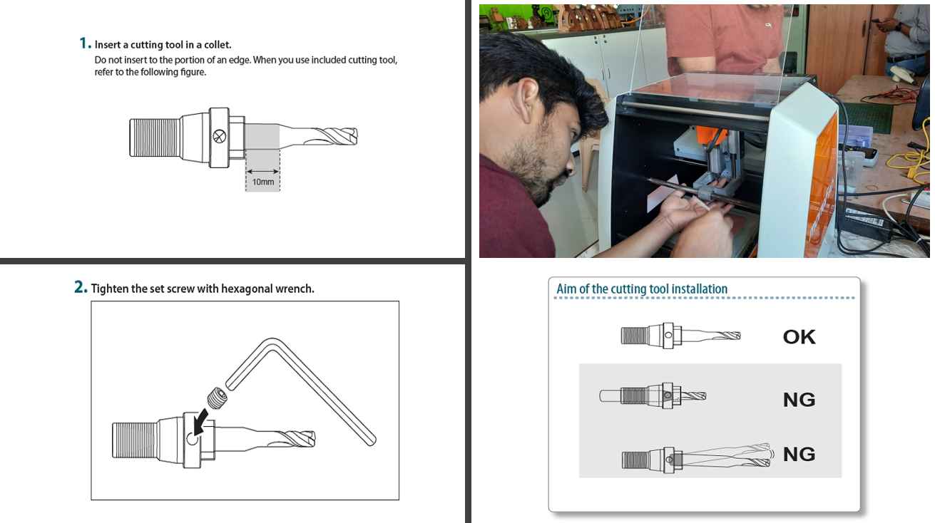
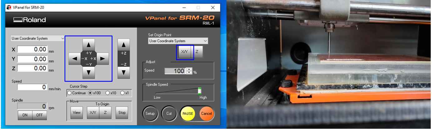
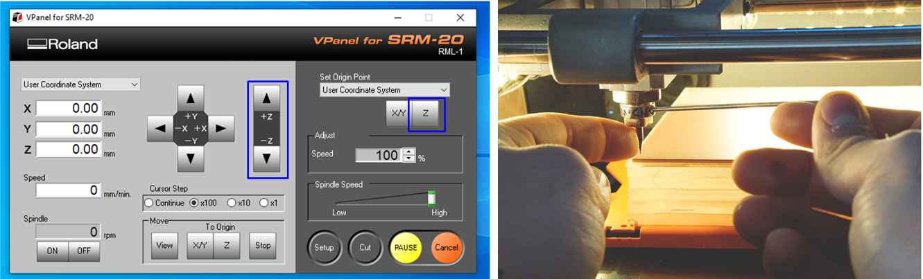
Seting-up the origin point of SRM-20(on X-Y plane)
As I set my bord in the middle of the machine bed I select the suitable place for cutting my PCB before starting machining I have to set the X-Y coordinate for the milling profile on my PCB board. For that, I use the arrow on the V panel to move the end mill tool and make it placed in a suitable position. at last, to set the X-Y coordinate I click the set XY button on the left side to set the origin.