7. Electronics design
Group assignment:
Use the test equipment in your lab to observe the operation of a microcontroller circuit board (in minimum, check operating voltage on the board with multimeter or voltmeter and use oscilloscope to check noise of operating voltage and interpret a data signal).
Document your work to the group work page and reflect on your individual page what you learned
Individual assignment:
Redraw one of the echo hello-world boards or something equivalent, add (at least) a button and LED (with current-limiting resistor) or equivalent input and output, check the design rules, make it, test it.
Optionally, simulate its operation.
GROUP ASSIGNMENT:
-
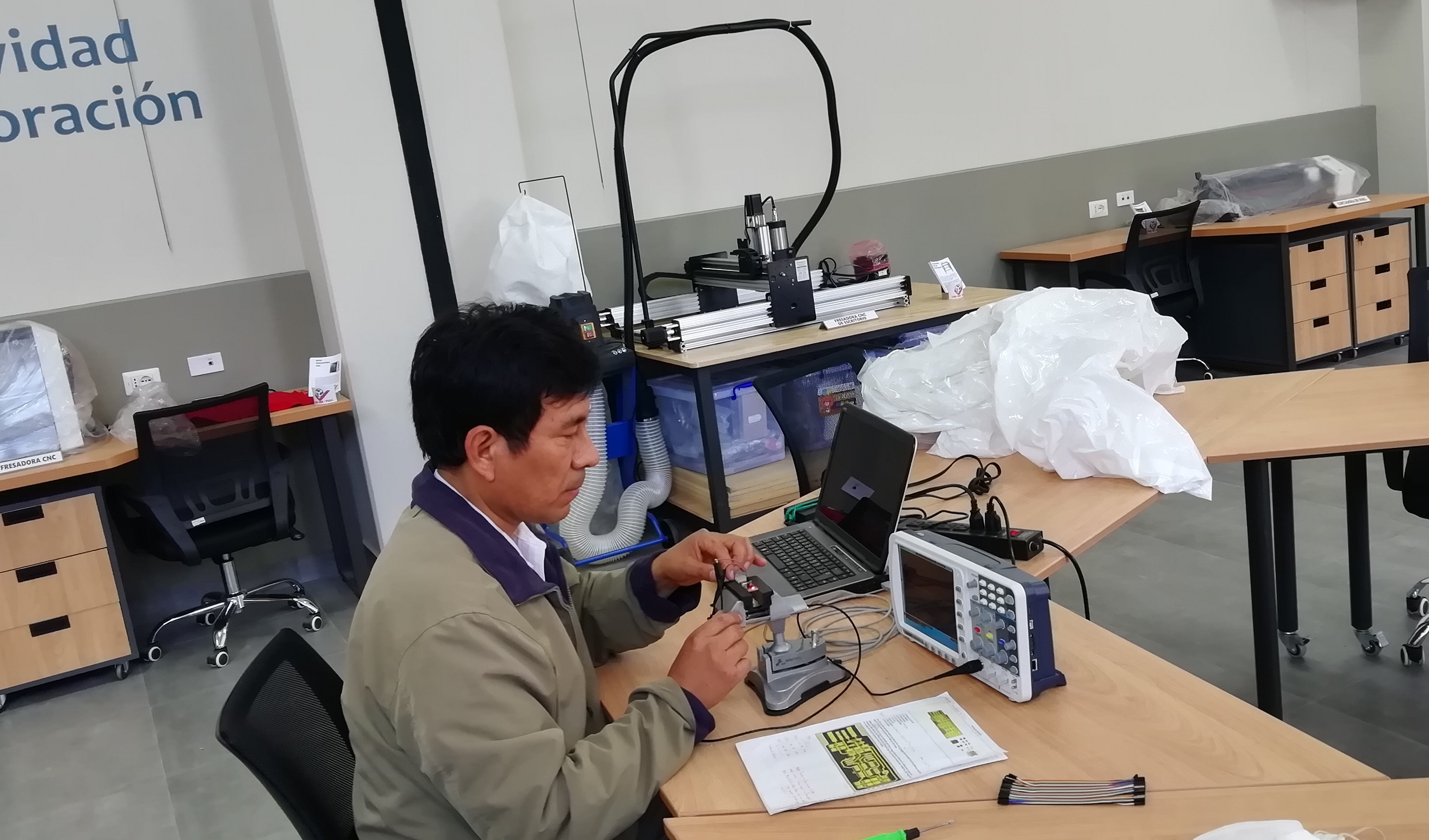
For the group task, we had to use two important instruments in the lab (multimeter and oscilloscope) to test the continuity or connectivity between the circuits, which is the multimeter; and to verify the signals, the digital oscilloscope. This would determine if we soldered the board correctly or not, thus allowing us to test the programming of the designed PCB.
-
In the FabLab Vigil we have a Unit-T brand multitester and a Owon brand digital oscilloscope.
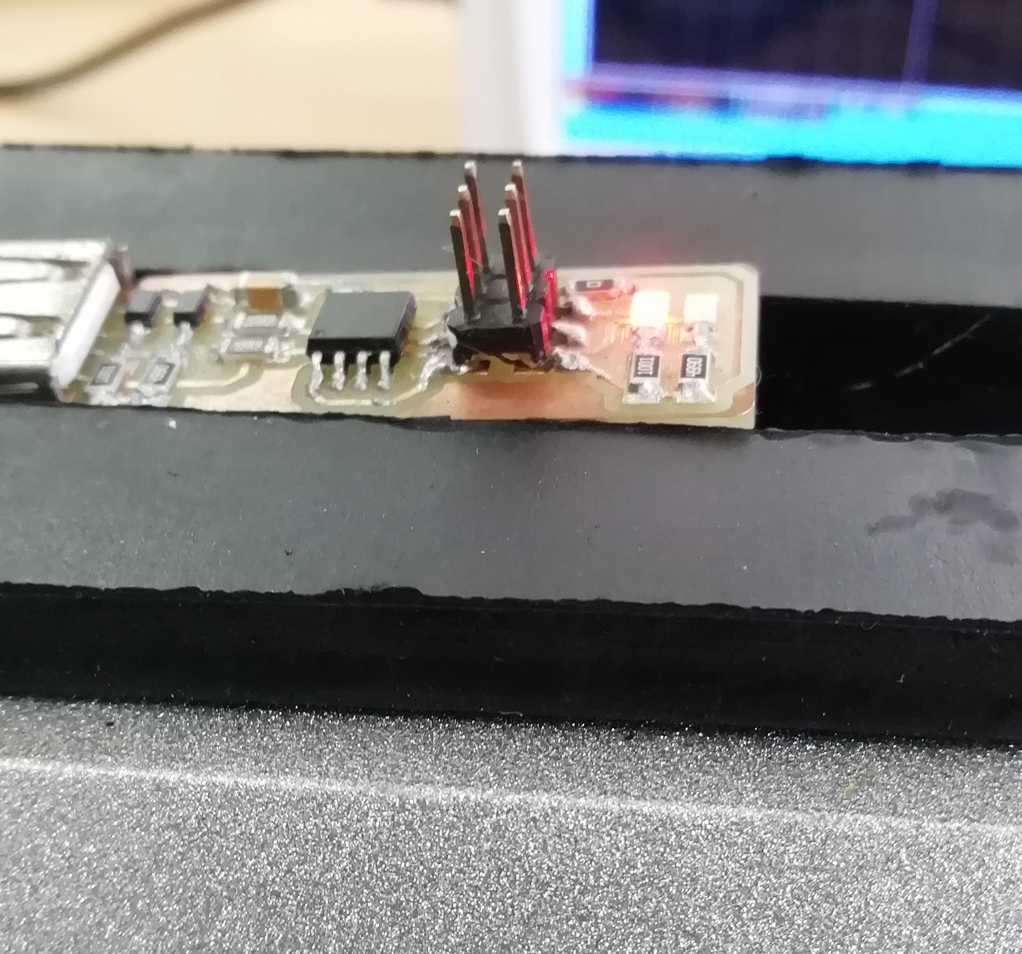
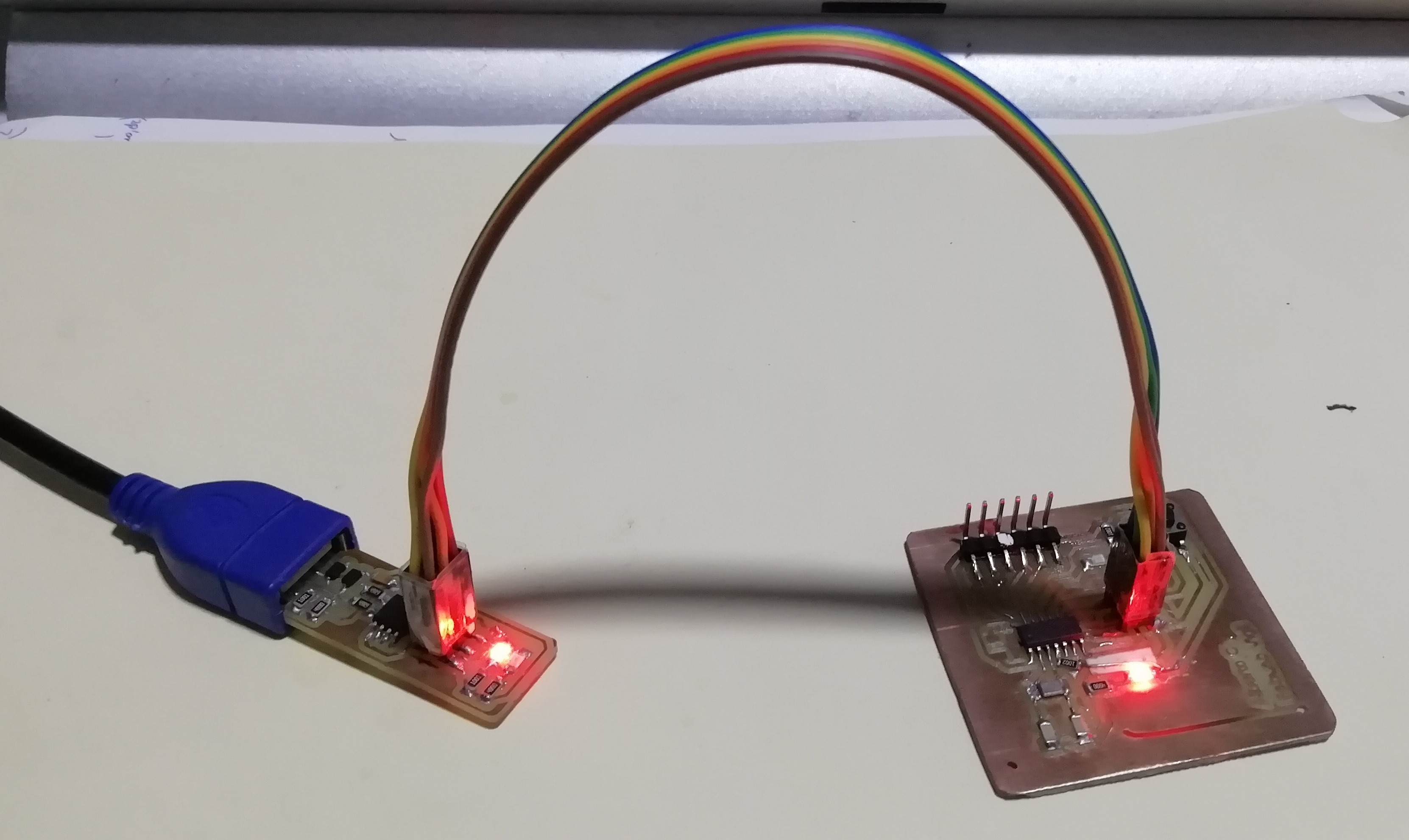
- Using the instruments is simple. What we did is measure the pulses of the ATTiny ISP card that we made in the previous assignment. We place the FabATTiny in the mini table vise and gently adjust it so that it cannot move.
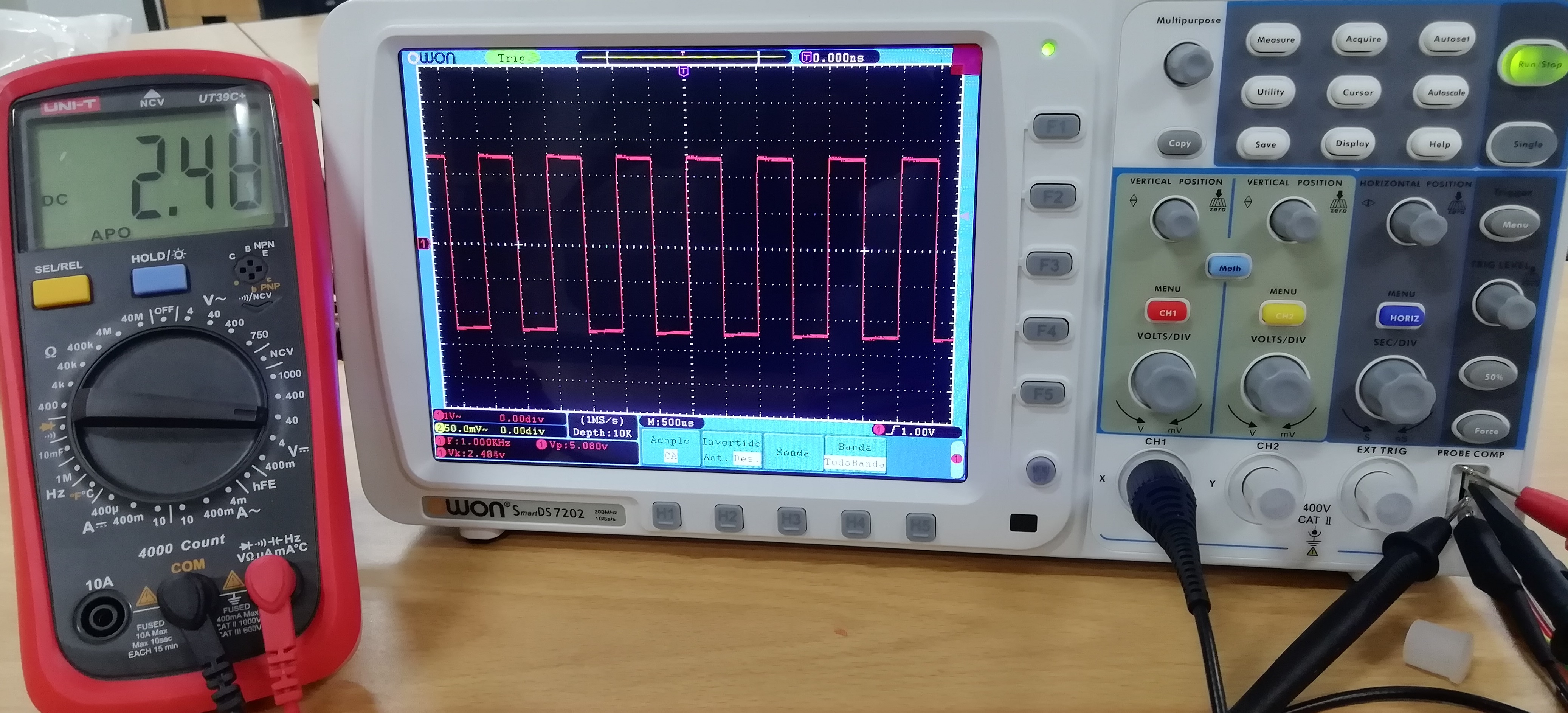
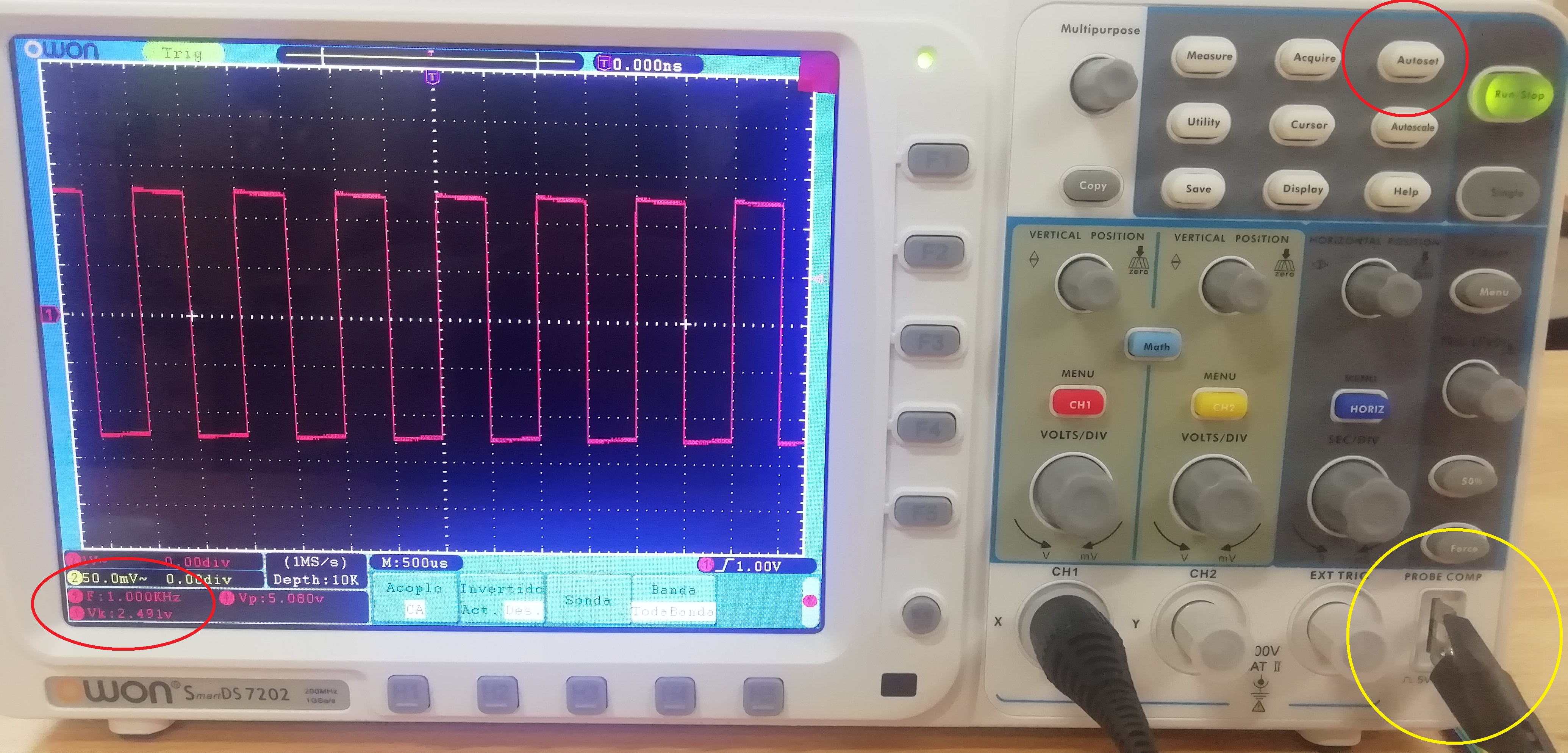
- Then I check the ends of the oscilloscope that are in 1X and place it in the PROBE COMP input of the oscilloscope. I press the Autoset button and manage to see the square signal of 1 KHz and 5.08 Vpeak (2.491 Vpp).
- I check the previous notes to see the programmed output of the LED that is oscillating, pin 3 corresponds to the output of the green LED. Pin 6 corresponds to GND (ground). It is there where I must connect the ends of the oscilloscope.
- I connect the leads of the oscilloscope and I can see the square signal in the FabISP.
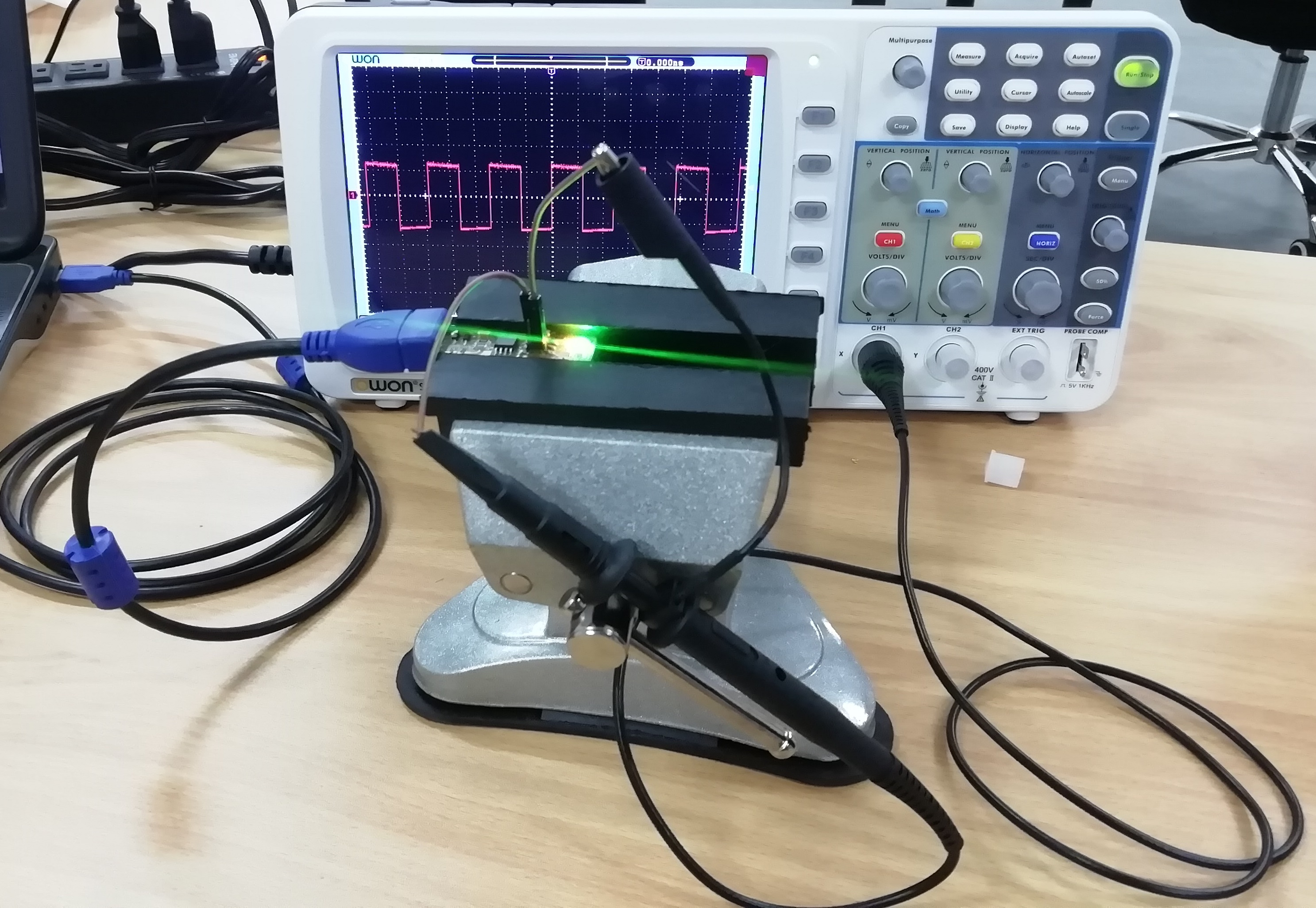
- I can see the LED turn on and off at 411 Hz frequency and 5.44 V amplitude.
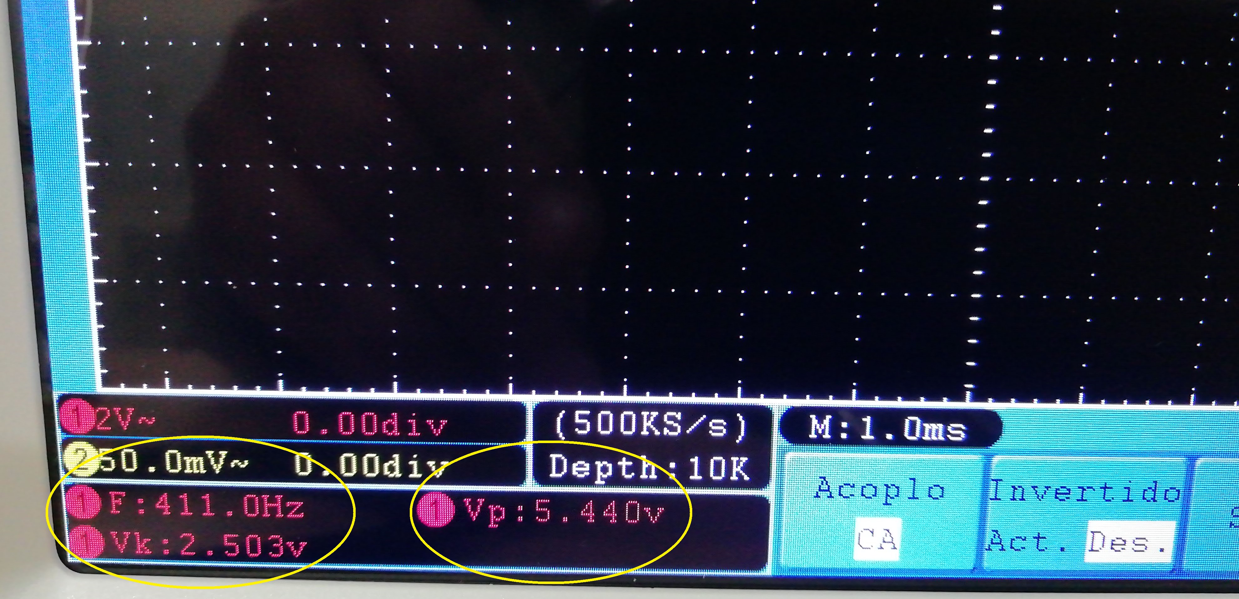
- I connect the tips of the Multitester in parallel to the tip of the oscilloscope and verify that the square signal measures 5.49 V. Previously I put the 40 V scale on the multimeter.
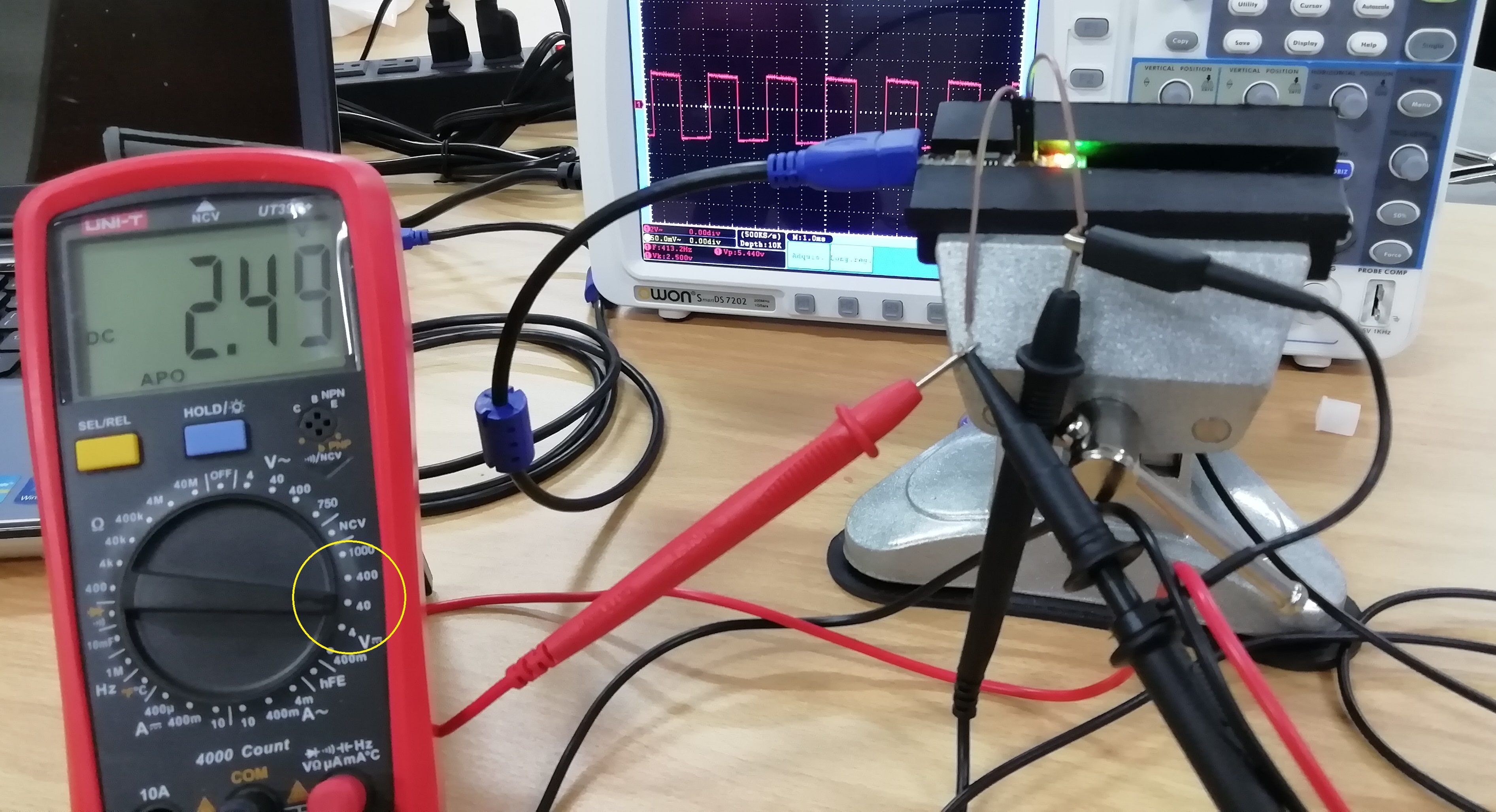
- Interesting to know that the LED turns on and off quickly that the eye cannot see.
- Check this video
INDIVIDUAL ASSIGNMENT
ATTinny44 microcontroller:
-
This high performance, low power AVR 8-bit microcontroller is perfect for simple boards. The CPU must be able to access memories, perform calculations, control peripherals, and handle interrupts. The on chip ISP Flash allows the Program memory to be re-programmed in-system through an SPI serial interface most commonly.
-
The ATTiny44/84 pin description is as follows:
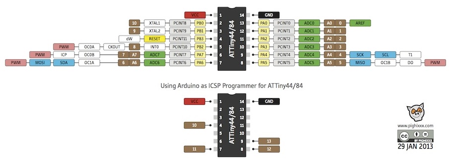
- I first made this design based on Neil G. Fab’s reference model Tiny ISP-Board.
PCB Design:
- For the PCB layout work with the Eagle IDE see 9.6.2. Previously I had worked with the Eagle 6.5.0 version. But I see that the current version is much more friendly in several aspects. For ease I add the eagle_fab.lbr library. I do this in the Control Panel.
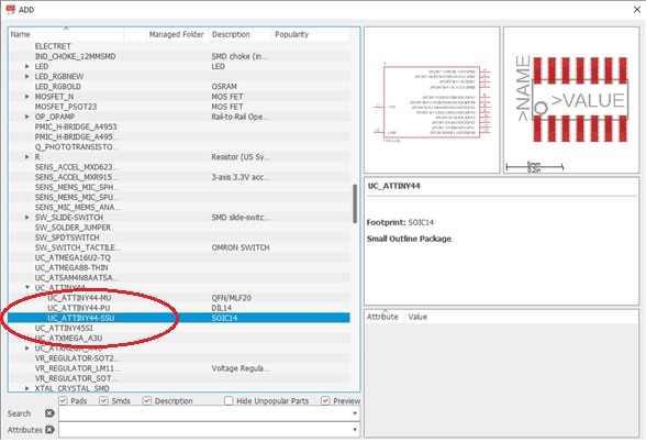
- I then add the necessary electronic devices and components to the PCB.
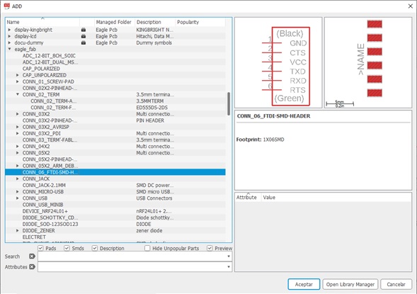
- I add the output FTDI terminals
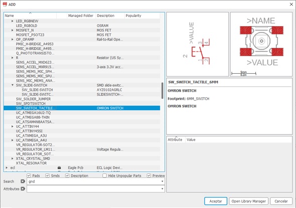
- I add the switch
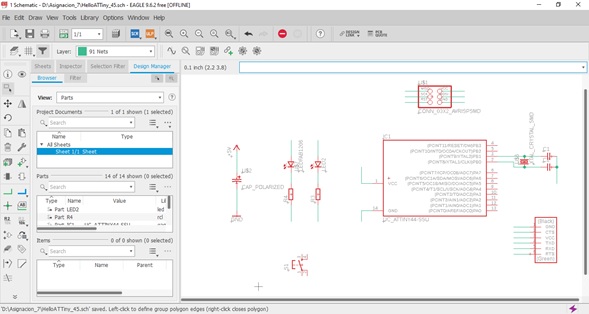
- After adding all the components, I already have the PCB schematic with the components, then it remains to order and wire it. This is how the design looks:
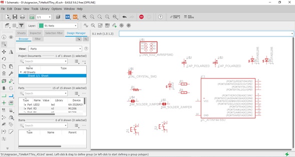
- With the Net tool I make the lines used for the connections
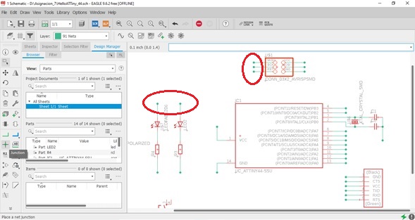
- Then I order and perform the distribution of the components
- Adding the join points
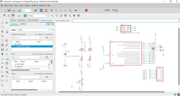
- Before finishing the schematic, it should appear like this:
- Then assign the label or name to the components with the Name tool.
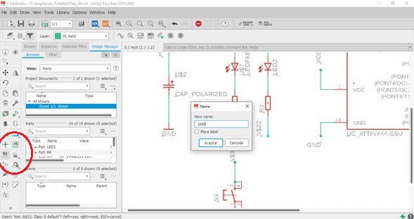
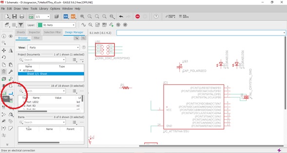
- He asks me to connect, I tell him YES
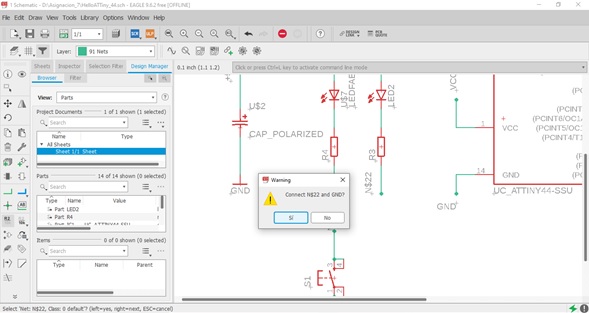
- I have all the GND grounds tagged.
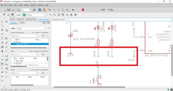
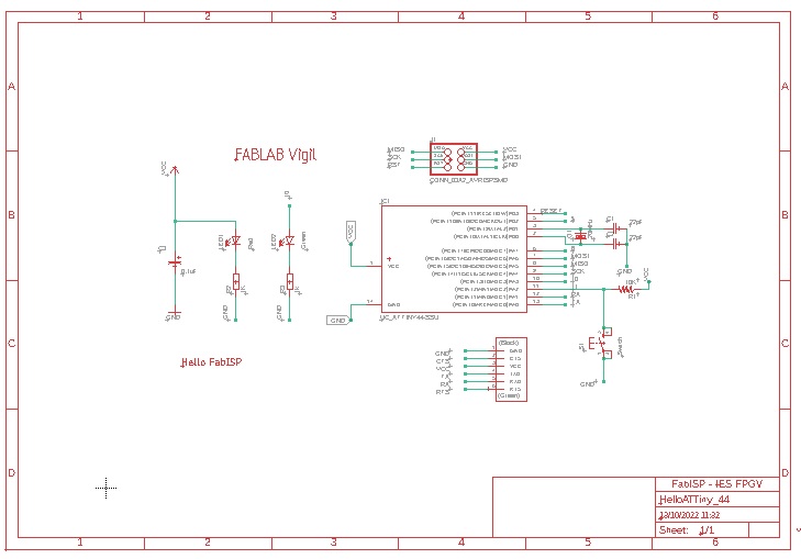
- The final schematic looks like this:
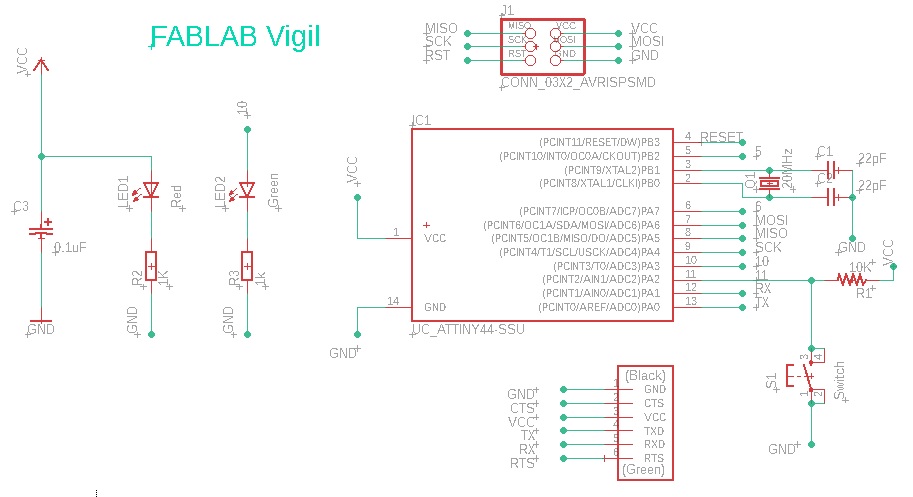
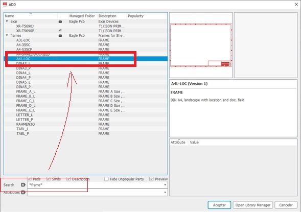
- To finish, I place a frame or legend box.
- This is what the final schematic looks like:
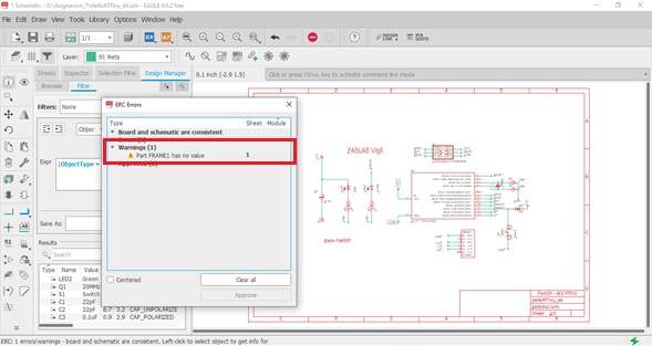
- Before converting to PCB I apply the ERC (Electric Ruler Checking) to the schematic. It throws me the following warnings:
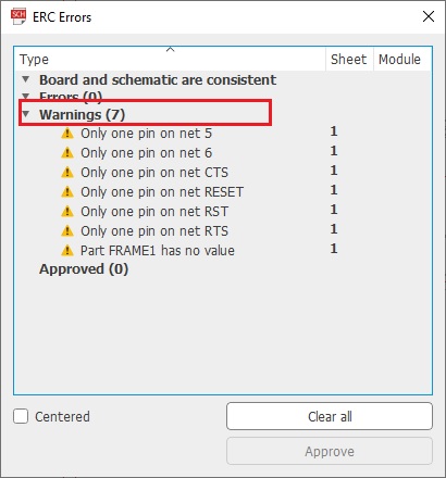
- I start correcting the Warnings one by one, before passing it to the PCB. Then it just throws me a frame hazard that doesn’t matter when moving to the PCB. Up to here, I already have the schematic is ready.
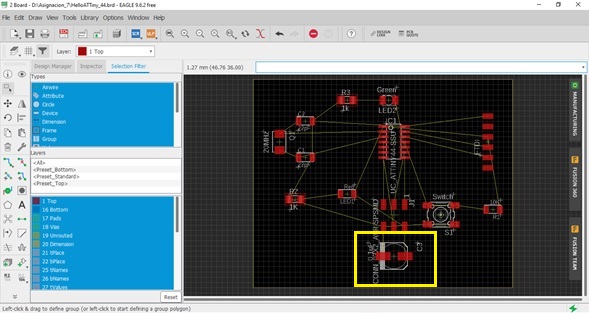
Board
- Then, I click on the BRD (Board) button to go to PCB (Printed Circuit Board) and start ordering the components
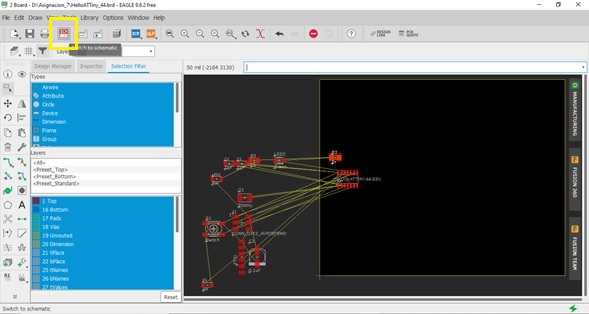
- Then I am accommodating the possible location of the components and help me with the rotation of the same. Take the location of the components based on Neil’s echo hello word board model.
-
I correct the size (footprint) of the capacitor C3 that came out very large. I change it for the SMD model.
-
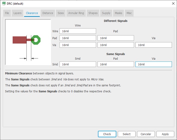
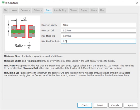
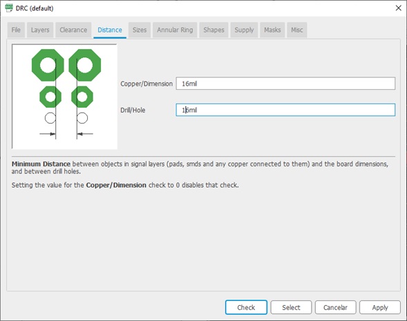
Add the set of layout rules (DRC) that help us like being the minimum free space between the components. You can add it in the Tool > DRC menu as shown below:
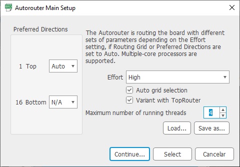
- In autorouting define only the Top layer and make 4 threads
- The distance will be 16 thousandths of an inch
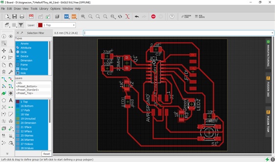
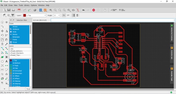
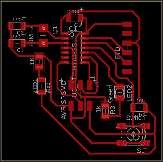
- I finally got the PCB layout
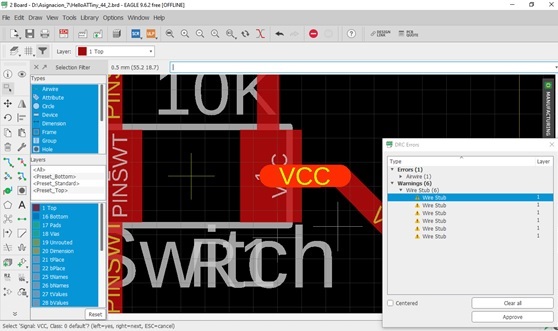
- The DRC alert me to 8 small pieces of wire that are loose. I am locating and deleting them one by one.
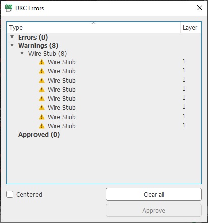
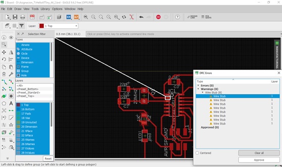
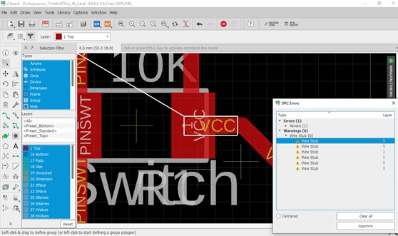
- Eliminate a small Vcc cable that is duplicated.
- This is the route of the tracks. I notice that I can reduce the size of the PCB by putting more components together.
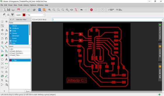
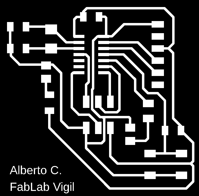
- The finished PCB would be as follows
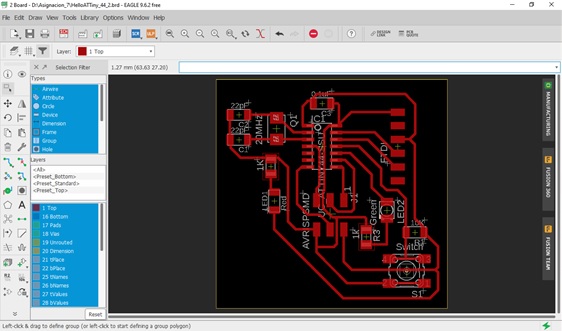
- I add a couple of labels and adjust the outline frame.
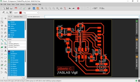
- I have the “Hello World” PCB ready
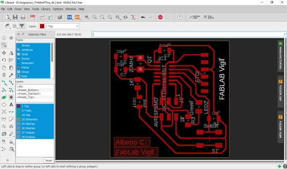
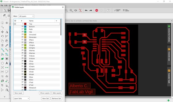
- I filter the top layer, for this I activate “Top” in the Eagle.
- Now I only see the copper face
- Then I import the PCB as an image file in .png format
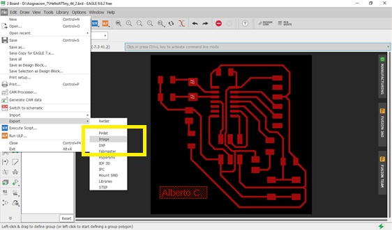
- Export with resolution of 500 dpi, size only of the full PCB and image in binary (monochrome)
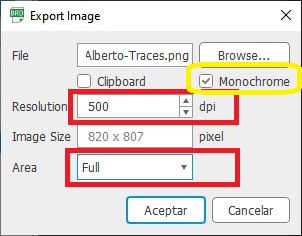
- In this way, I get the PCB in real size

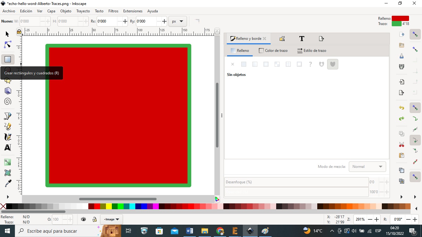
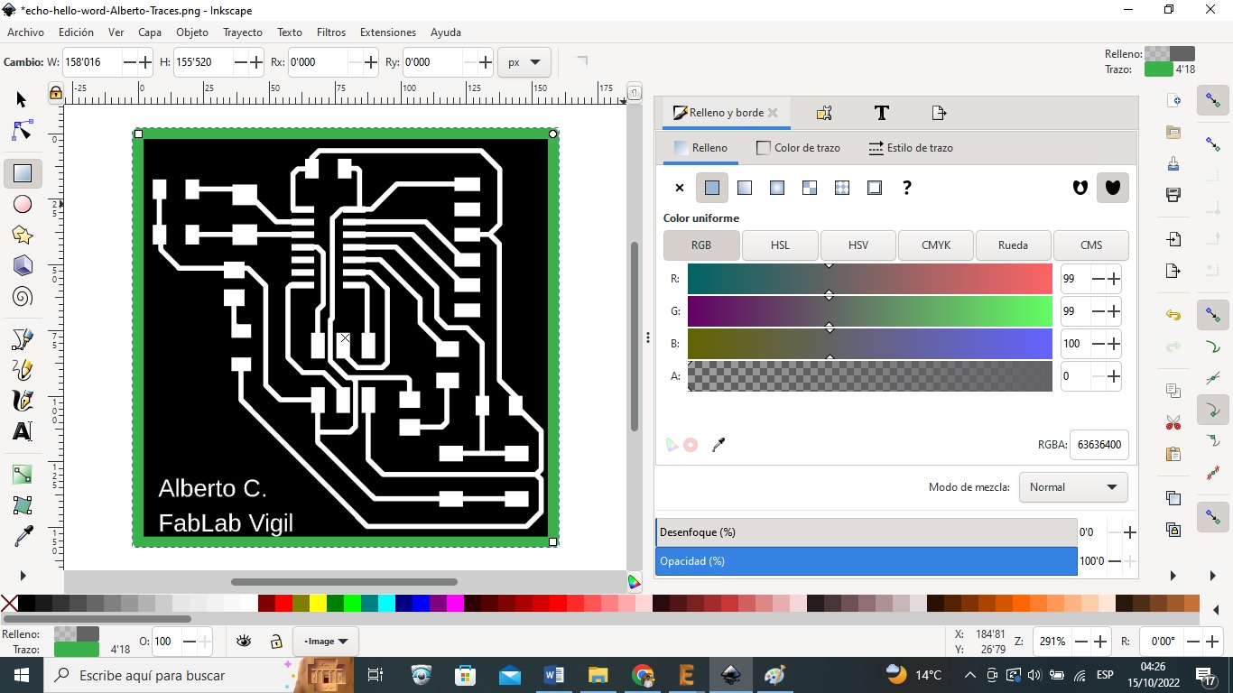
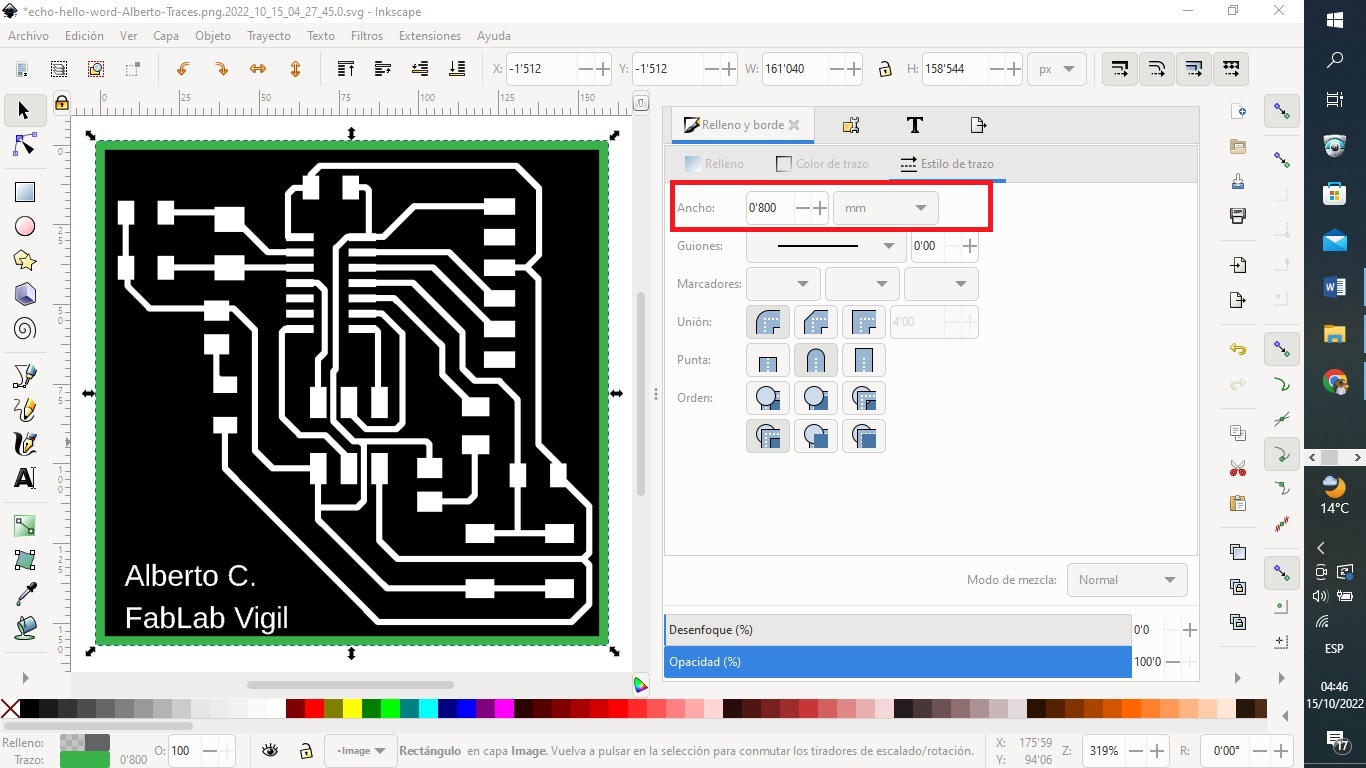
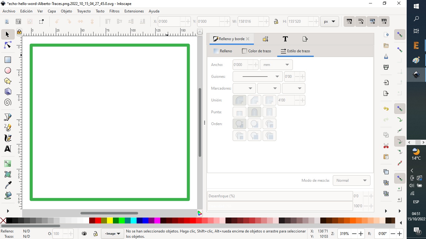
- To cut the board I create the PCB outline, for this I used Inkscape software
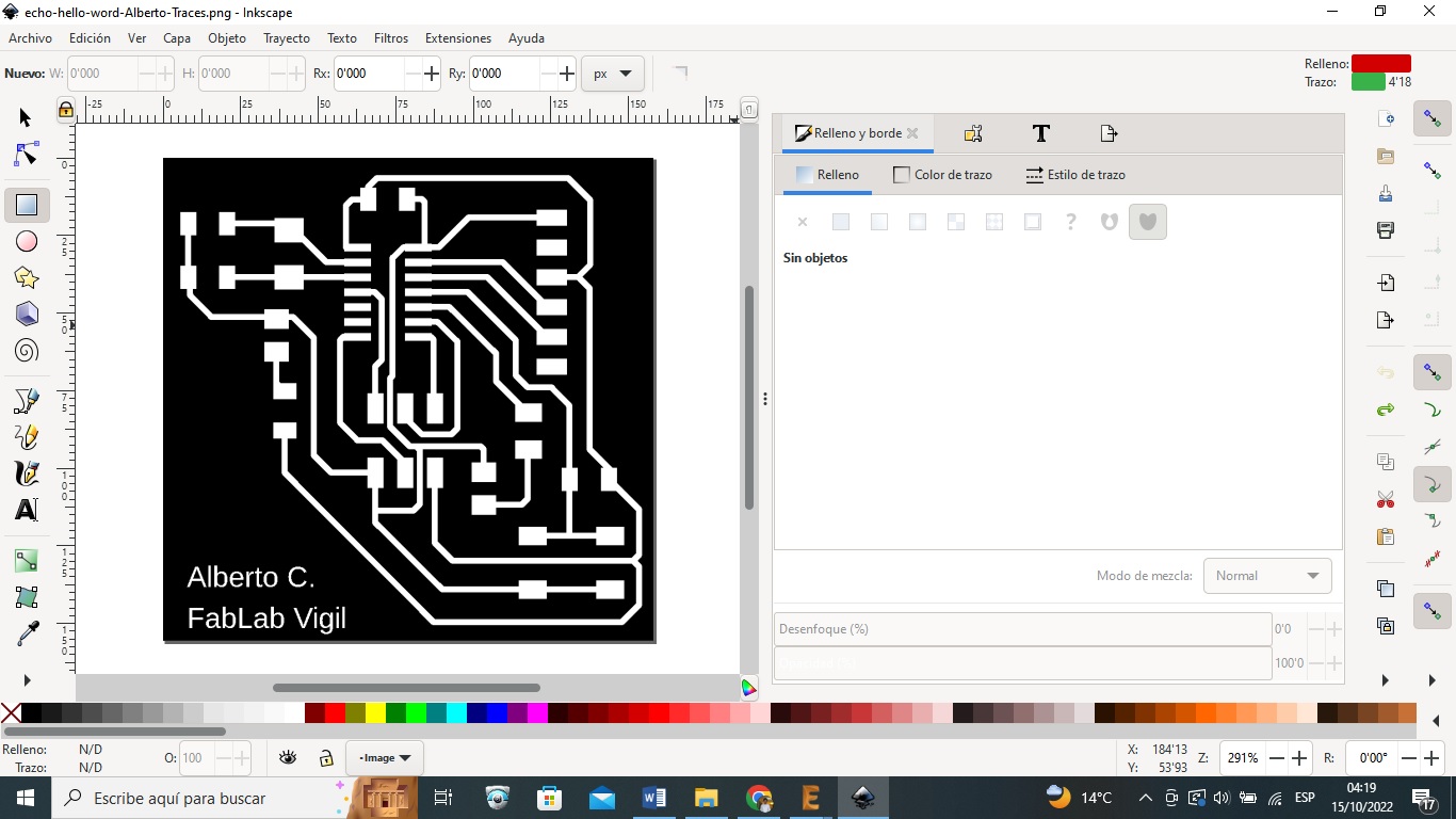
- I apply a square around the traces.
- I remove the filling.
- I give it a thickness of 1/32 inches equivalent to 0.8 mm
- I erase the image of the PCB, so that I only have the outline trace
- I give it black color to export it as monochrome.
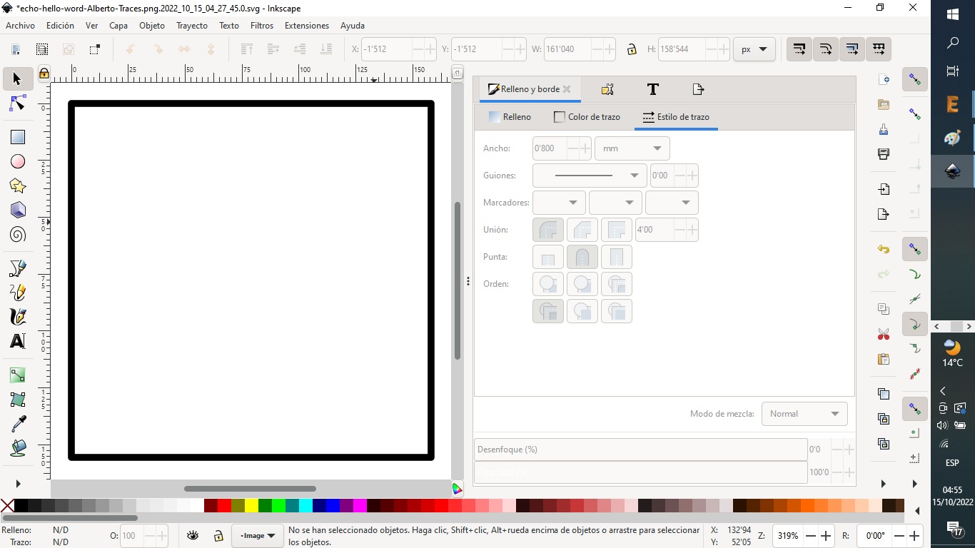
- This is how I have the Outline

- I only have to obtain the .rml files to manufacture it in the Monofab.
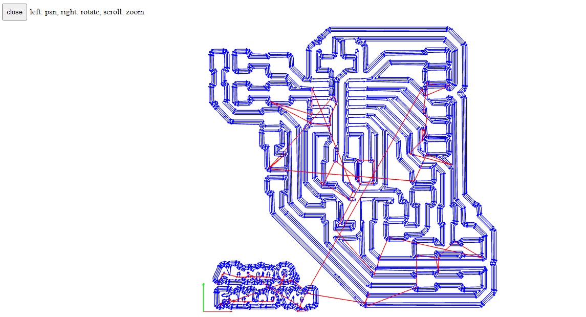
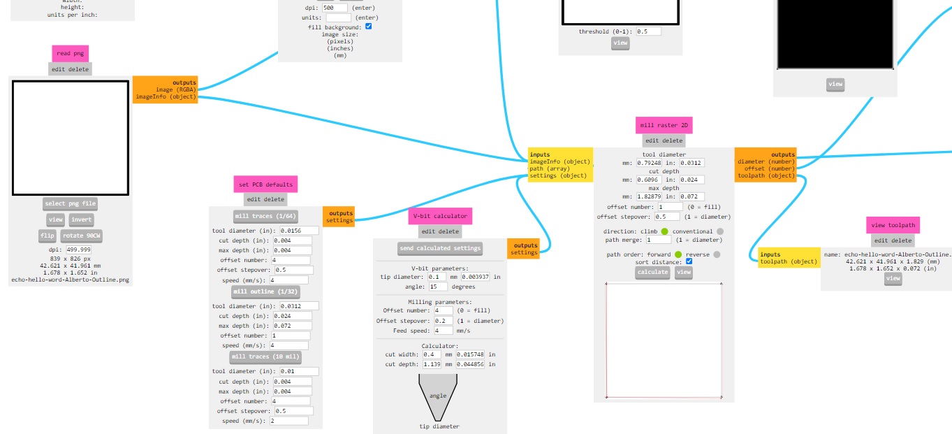
Modsproject:
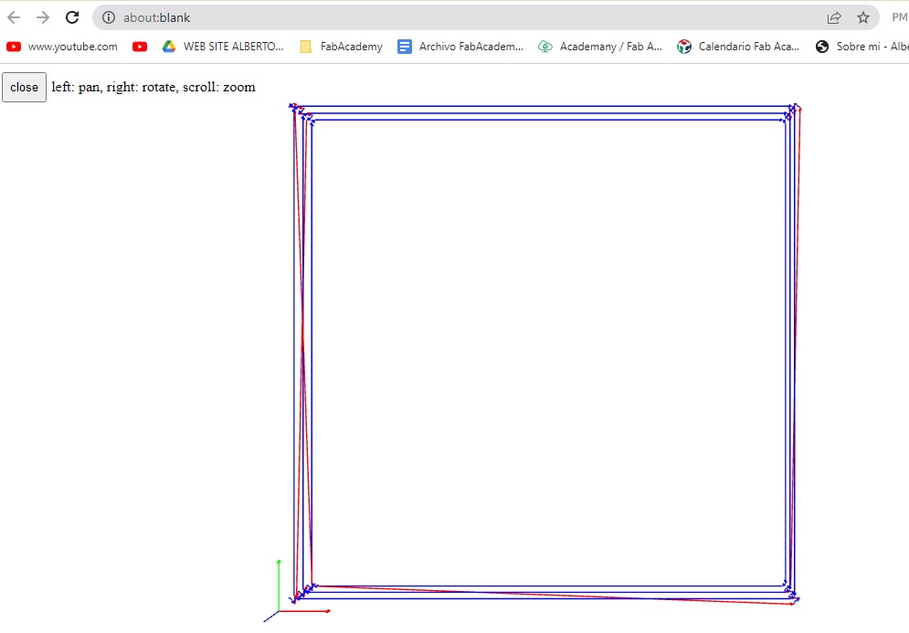
- I used modsprojec online at FabModules to load the .png images successively and generate the G code for the Rolland CNC mill to mill the traces and mill the outline shape of the PCB I have designed. I follow the protocols of the assignments 5.
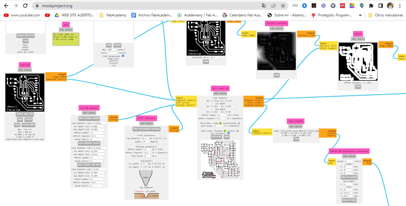
- For the outline
PCB fabrication:
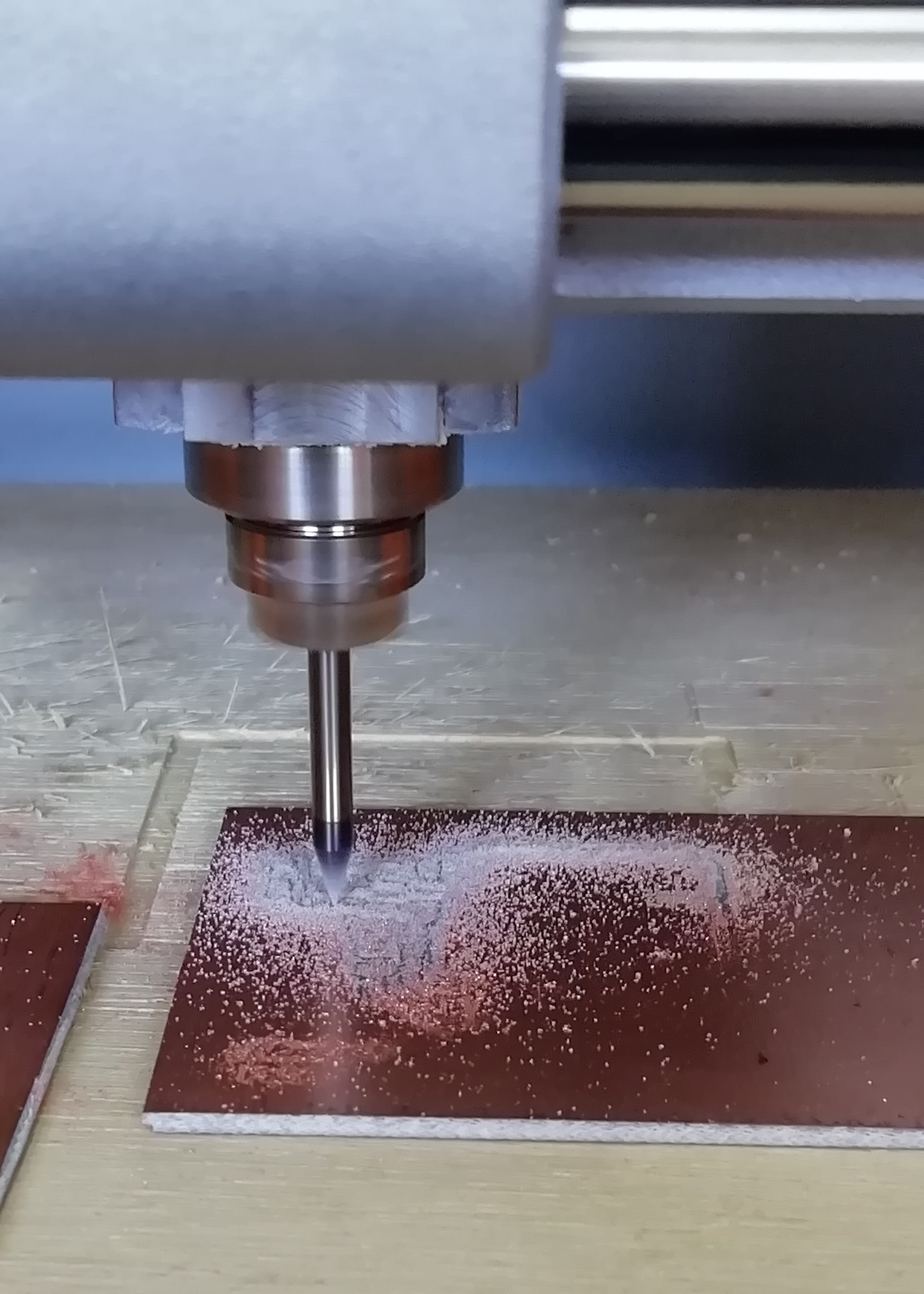
- I turn on the Monofab and load the generated .rml extension files and start milling
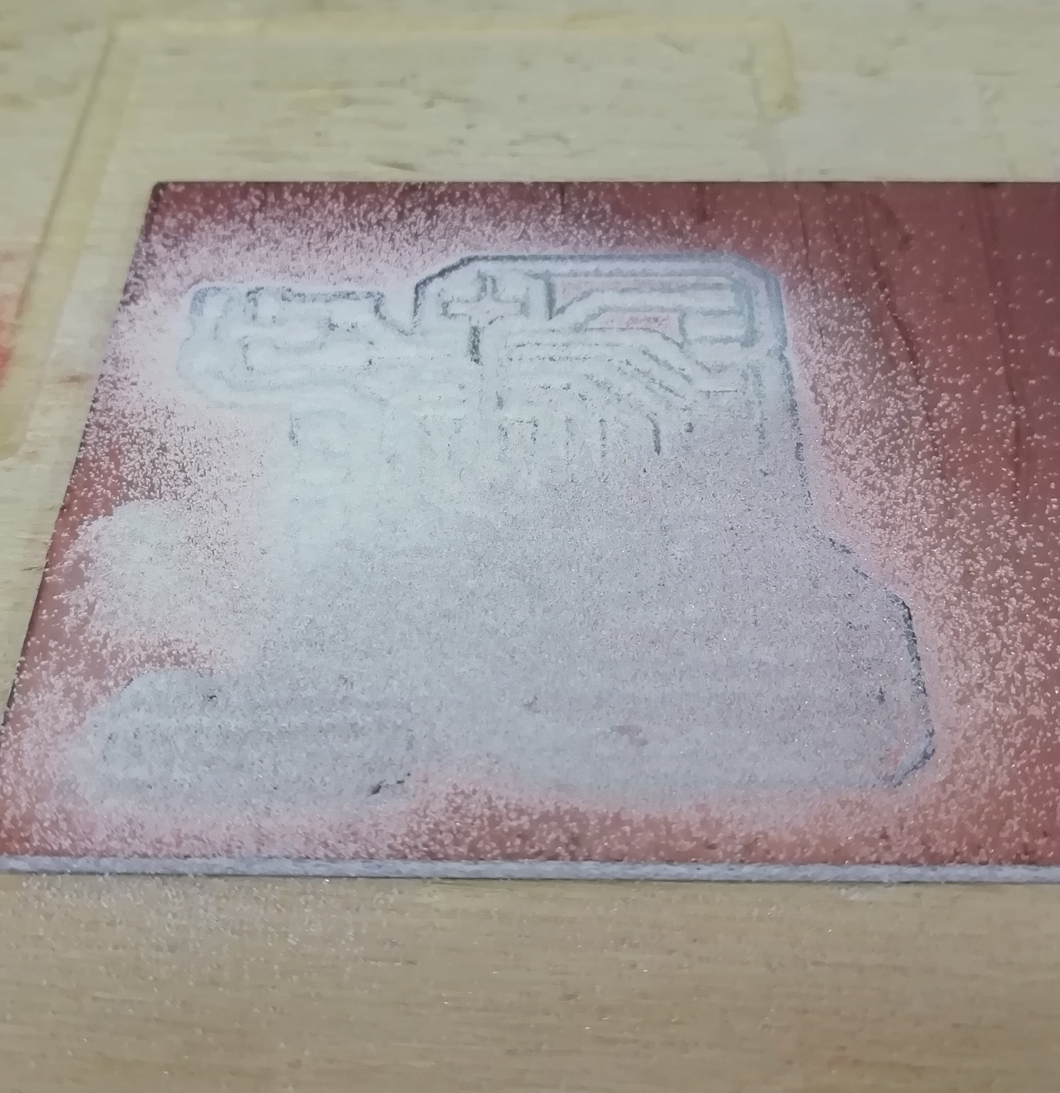
- I subtract the nickelite residues.
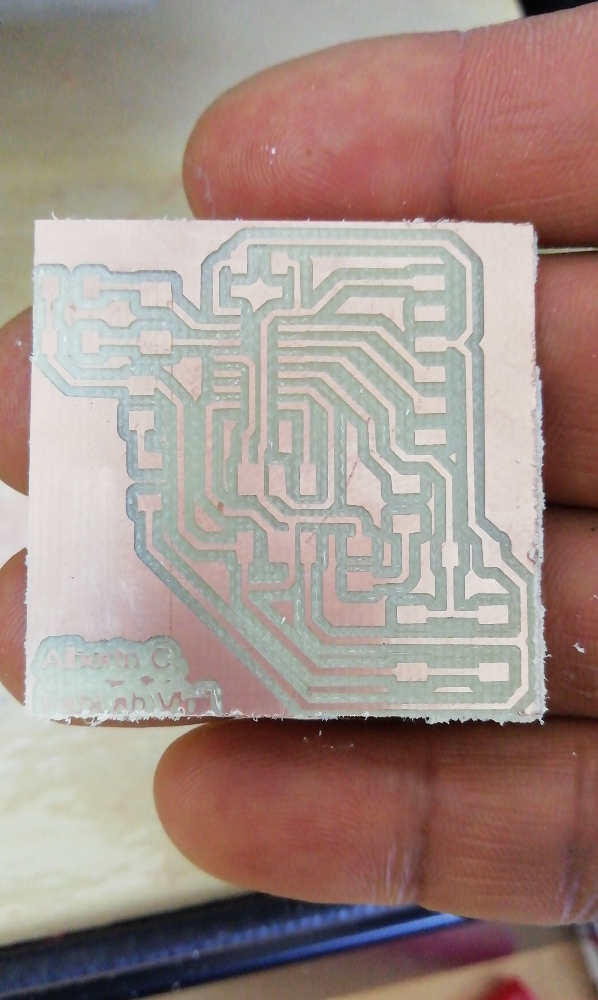
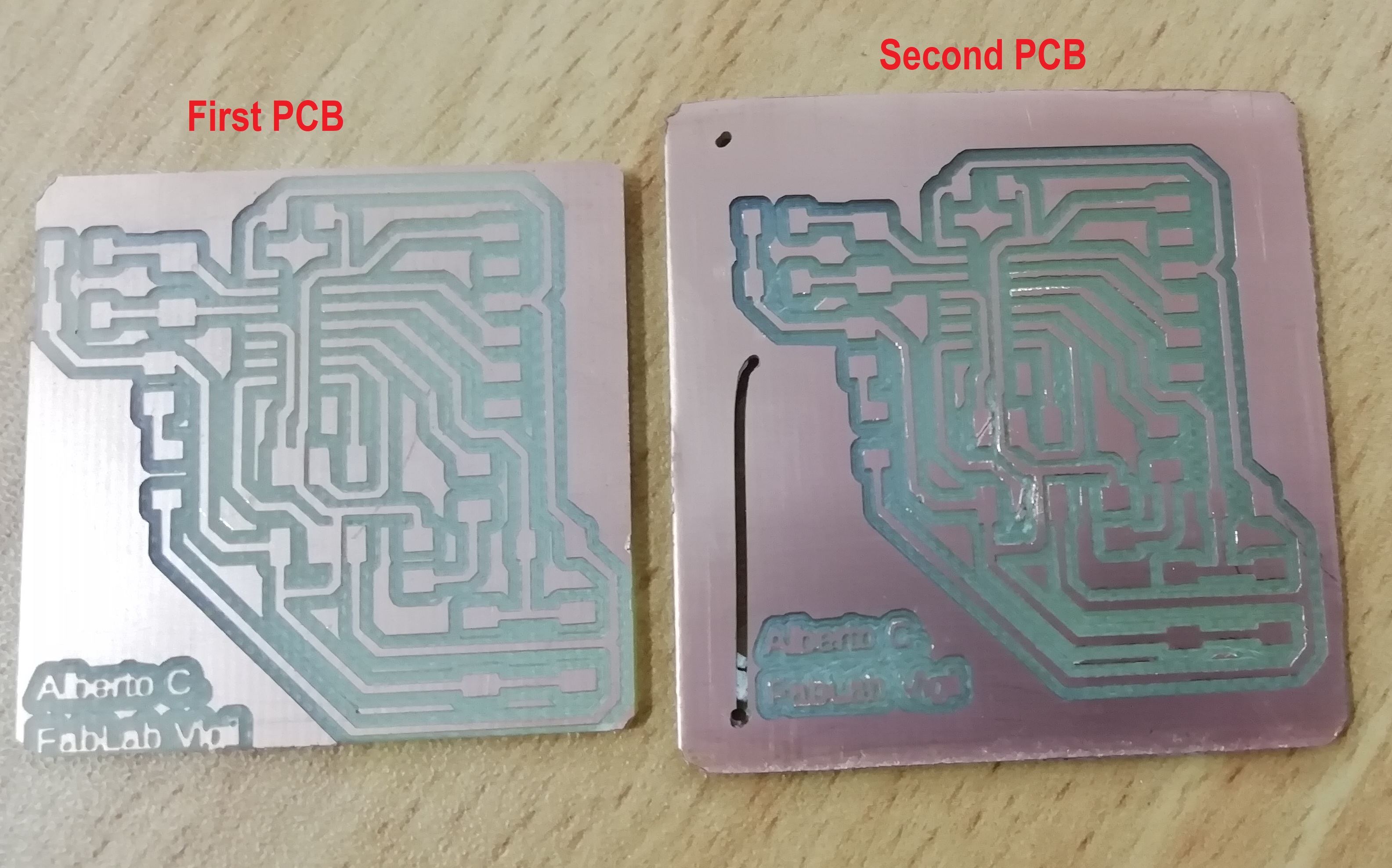
- In this first PCB the outline was too tight. I will make another improved one.
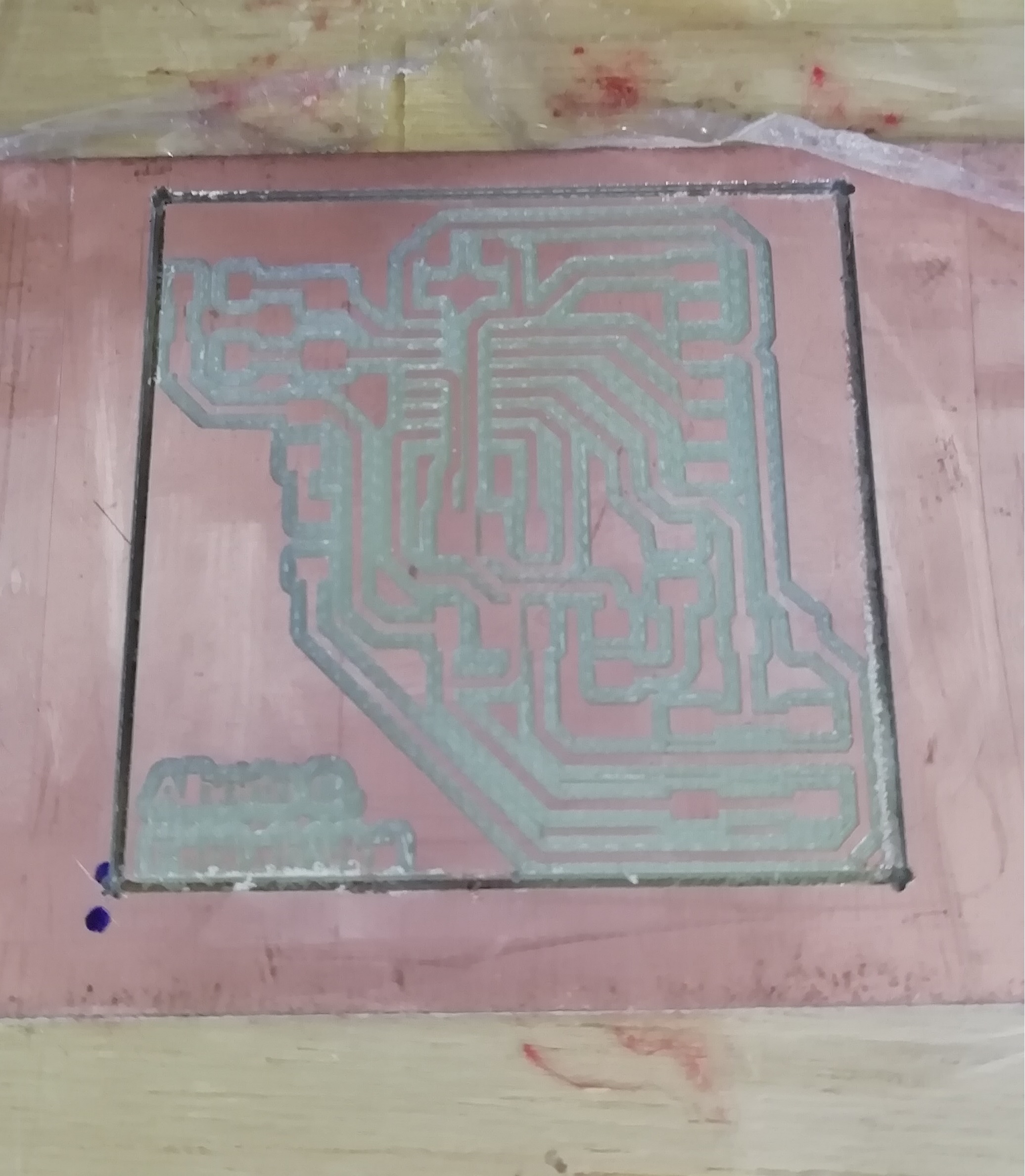
- This is the second PCB, it looks better than the previous one. I will keep this one.
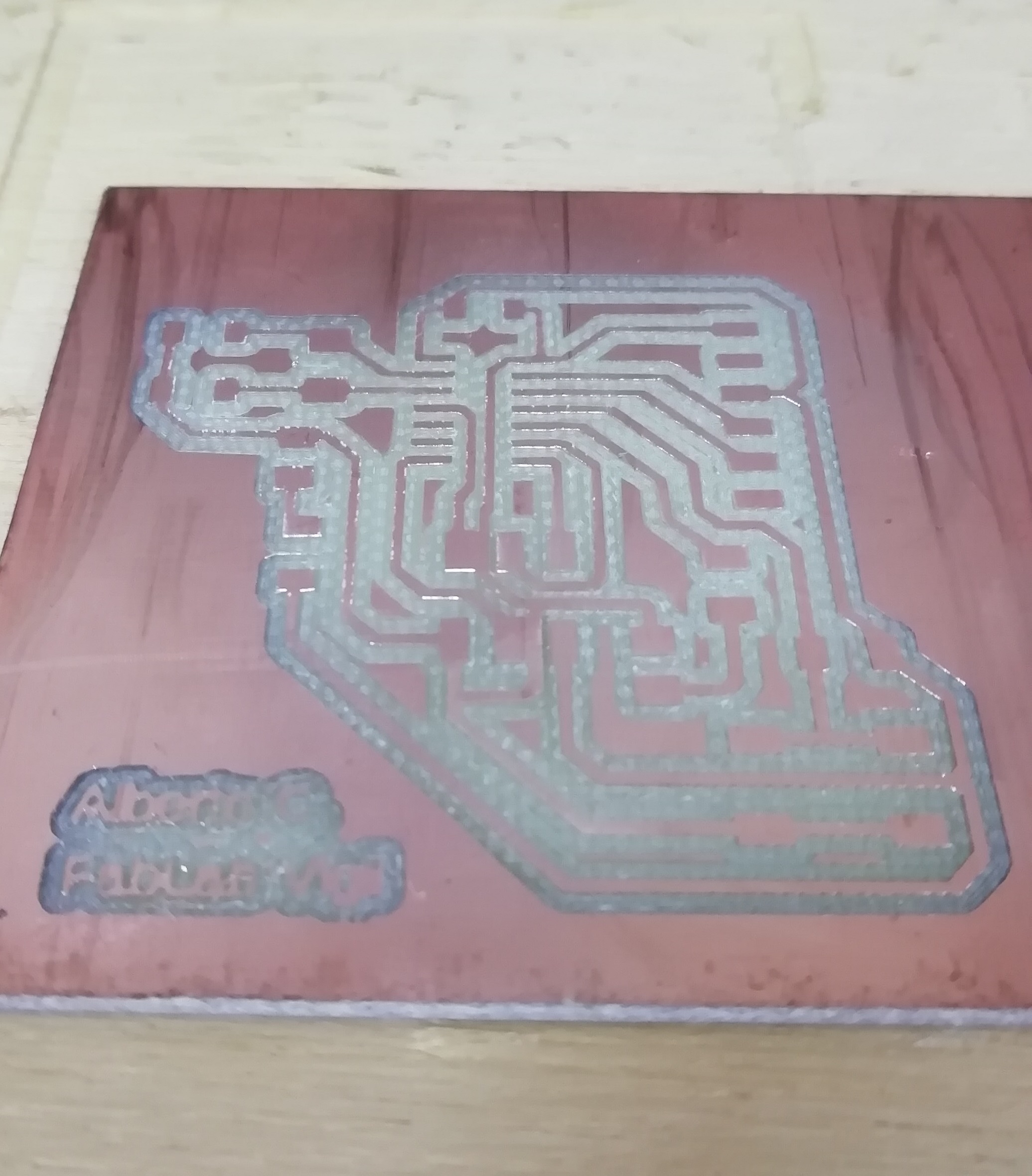
- I managed to fabricate 2 PCB boards. On the first PCB I made the outline too small. I will try the second PCB for soldering.
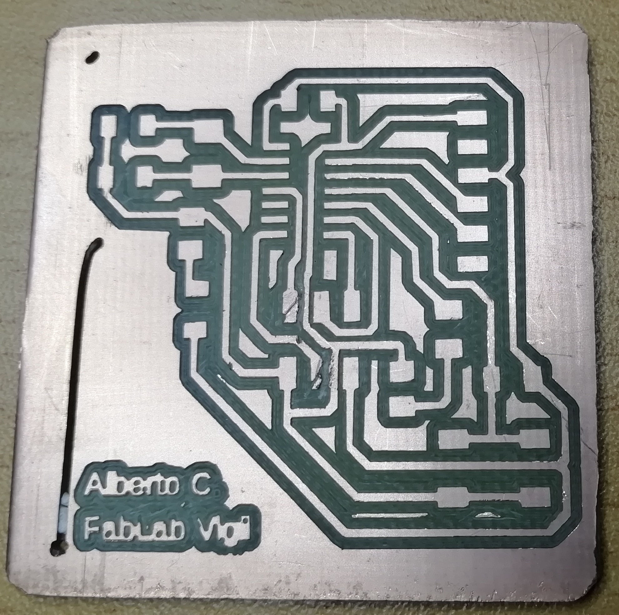
- I finished milling my hello board and it looks good so far. The next step is welding.
- This is a short video of the milling process:
Final board
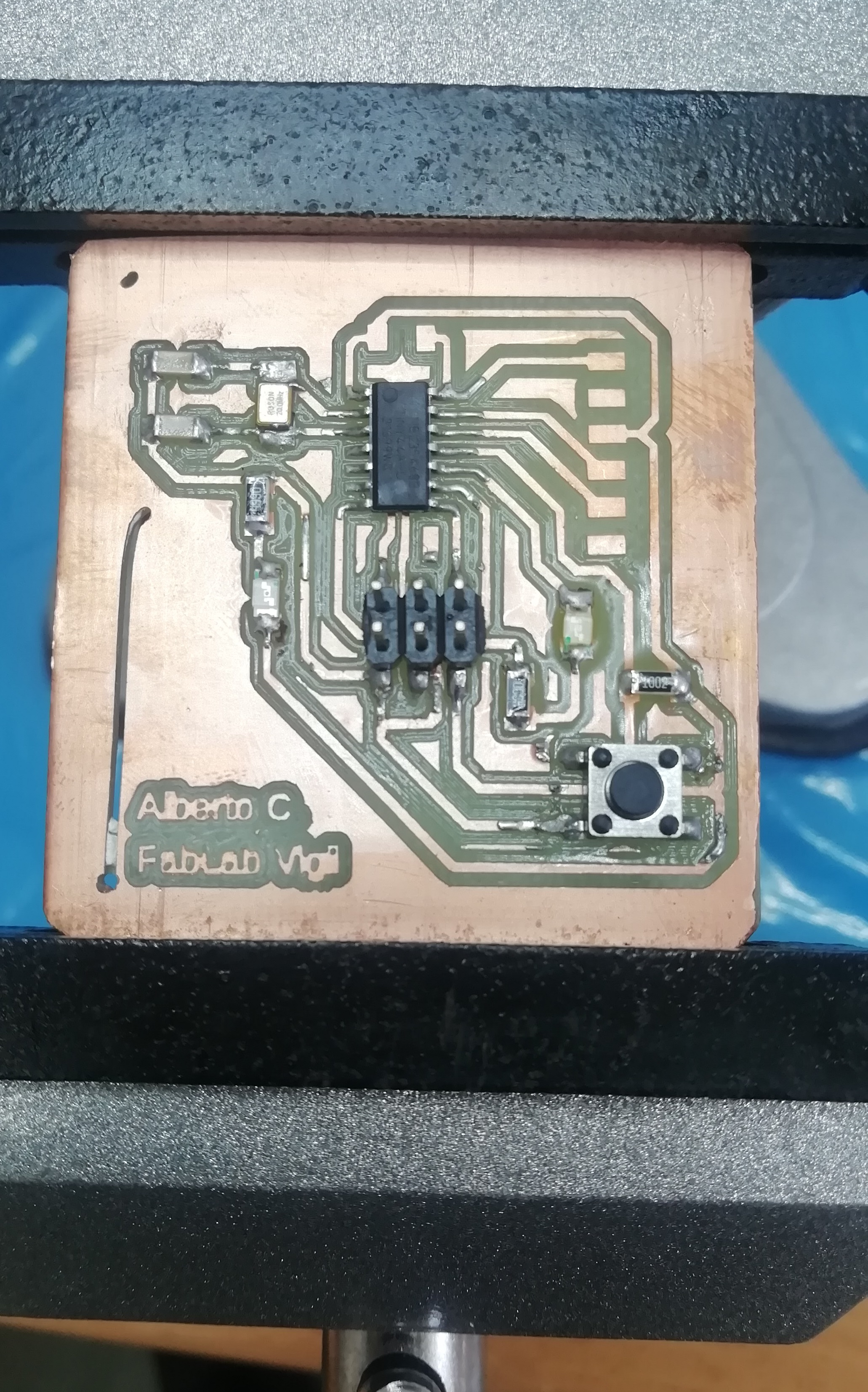
- I soldered the components, this is the final result. Now it is ready to be programmed.
- The FTDI connector is missing.
- The PCB is ready to be programmed.
Programming
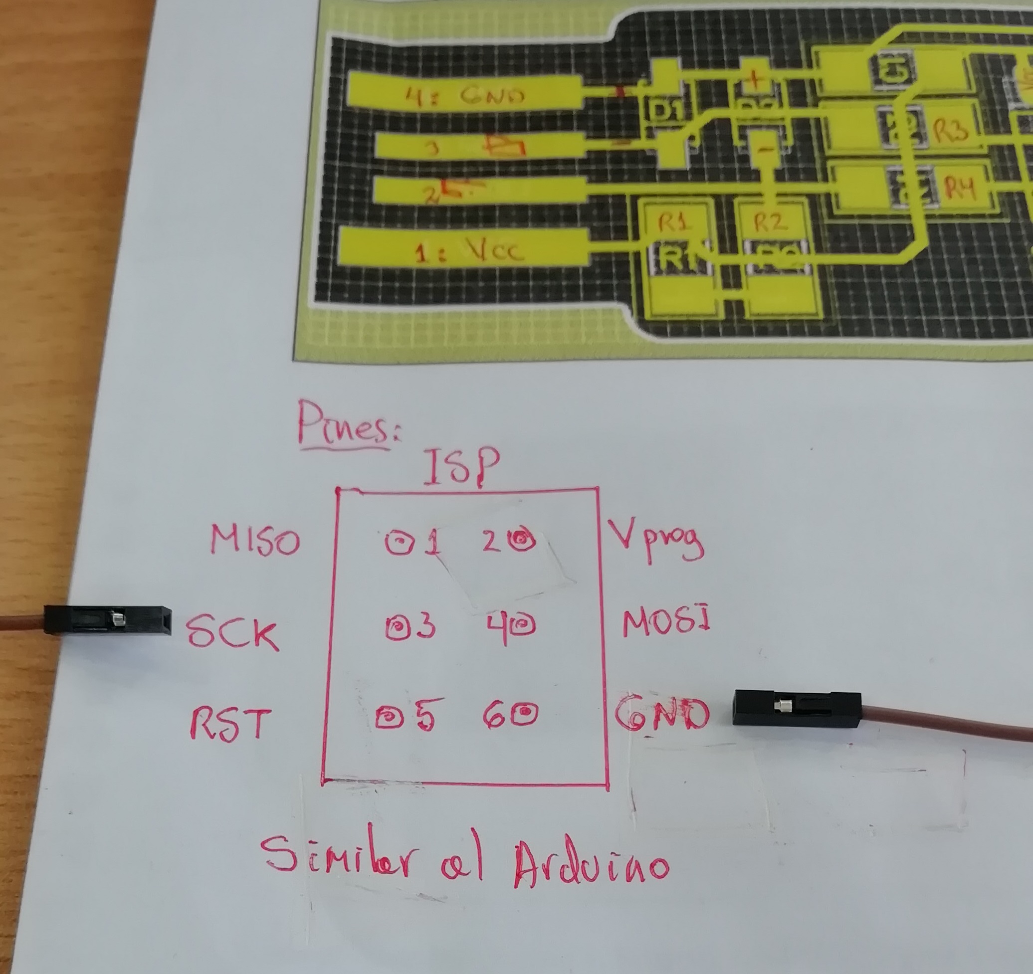
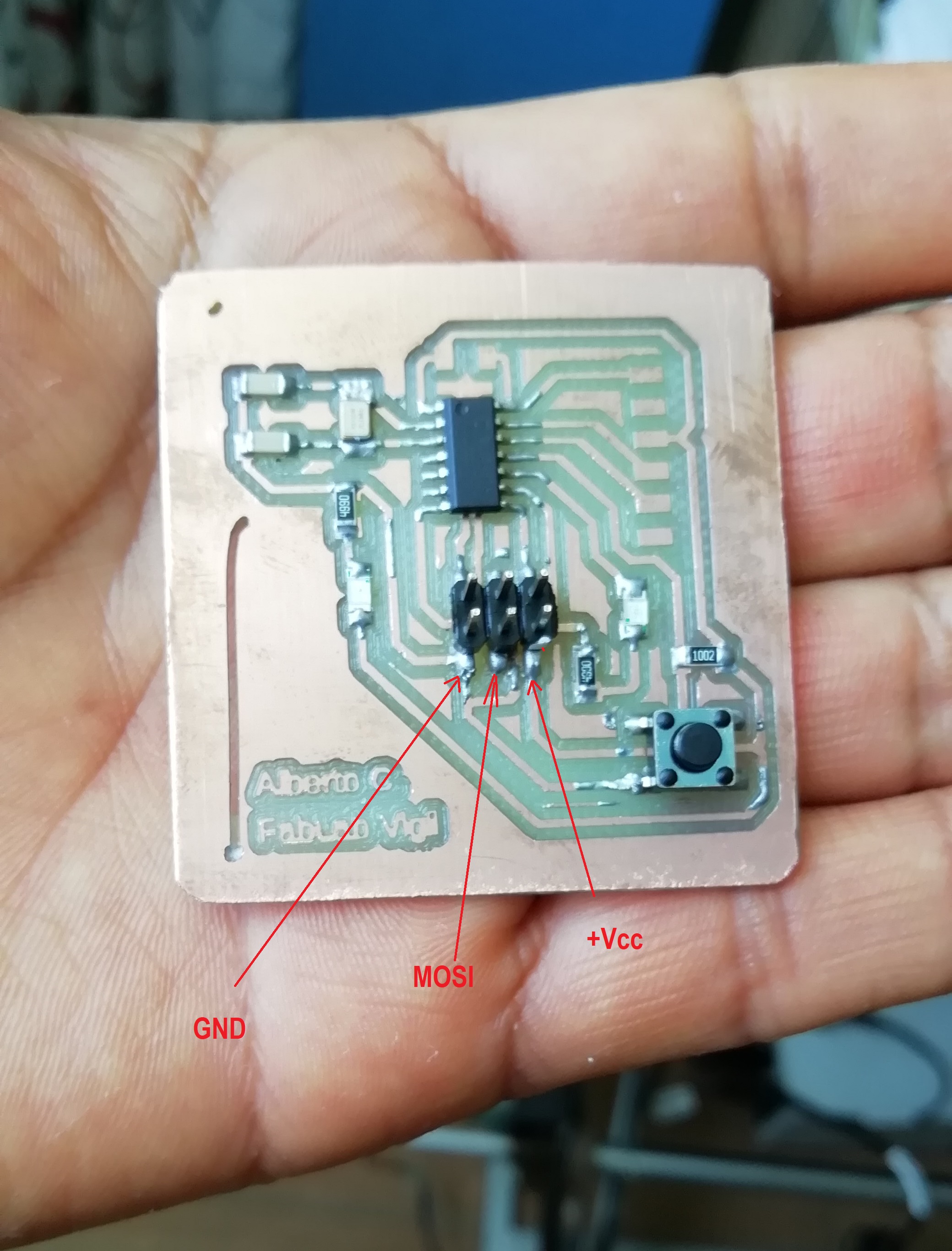
- To program use the FabISP from the above assignment. Connect the FabISP Programmer to the Hello ATTiny 45 board. The ISP connectors on both boards have the same pin configuration.
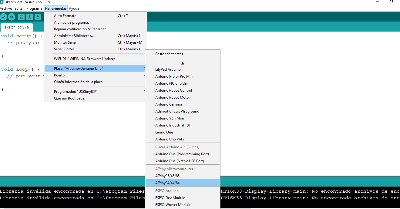
In the Arduino IDE, I go to tools and select ATtiny44 board and processor.
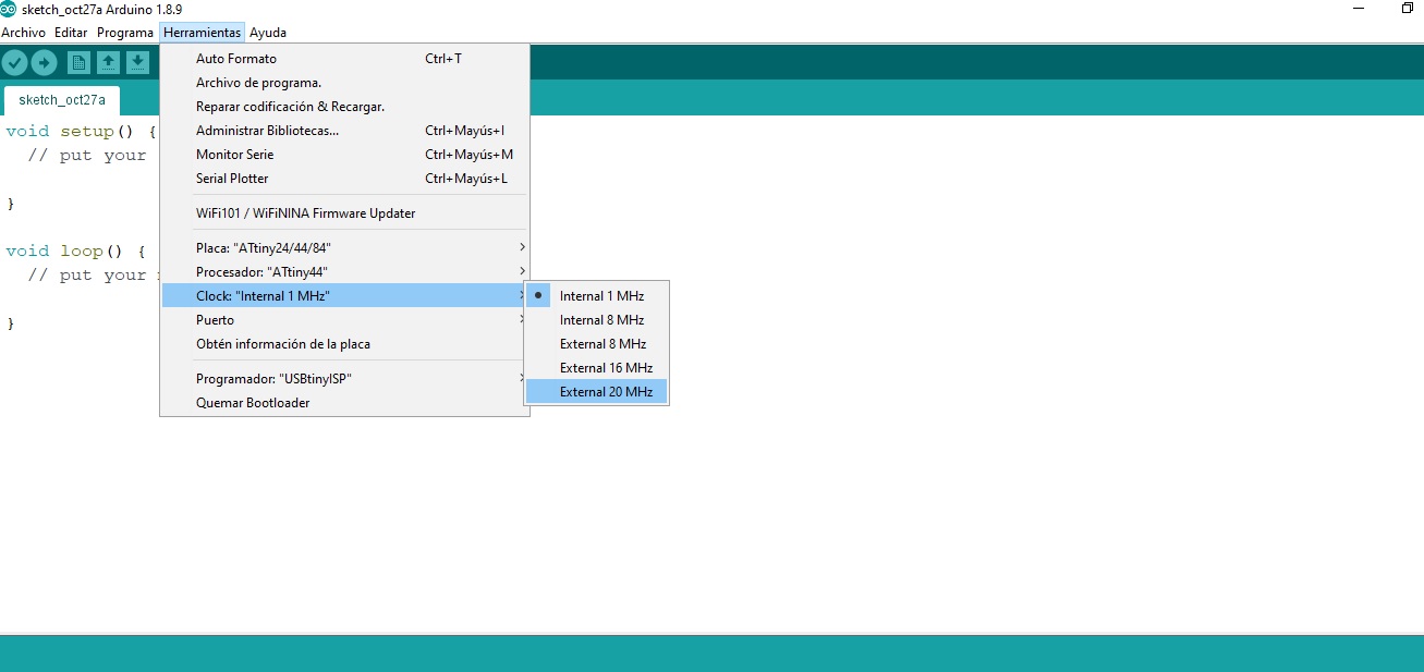
- The crystal I used for the PCB is 20 MHz, so I select 20 MHz external relog.
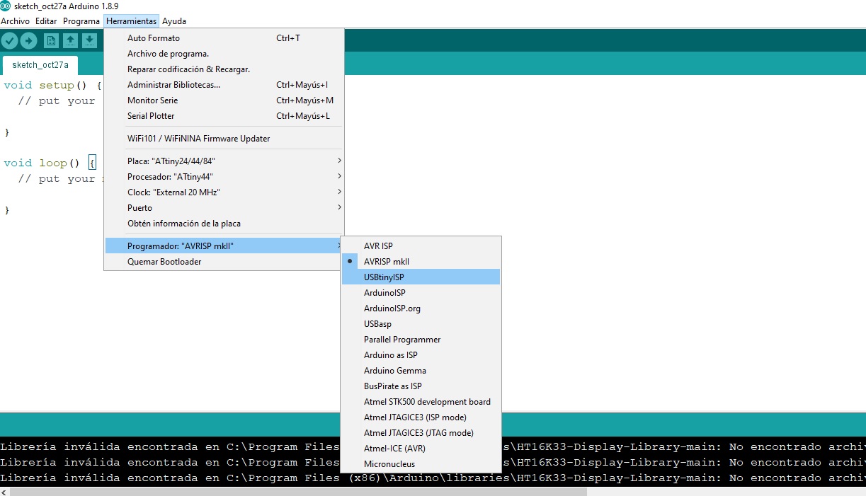
- Next, I have to transfer the “Hello ATTiny44”, for this I chose the FabTinyISP Programmer in USBtinyISP mode.
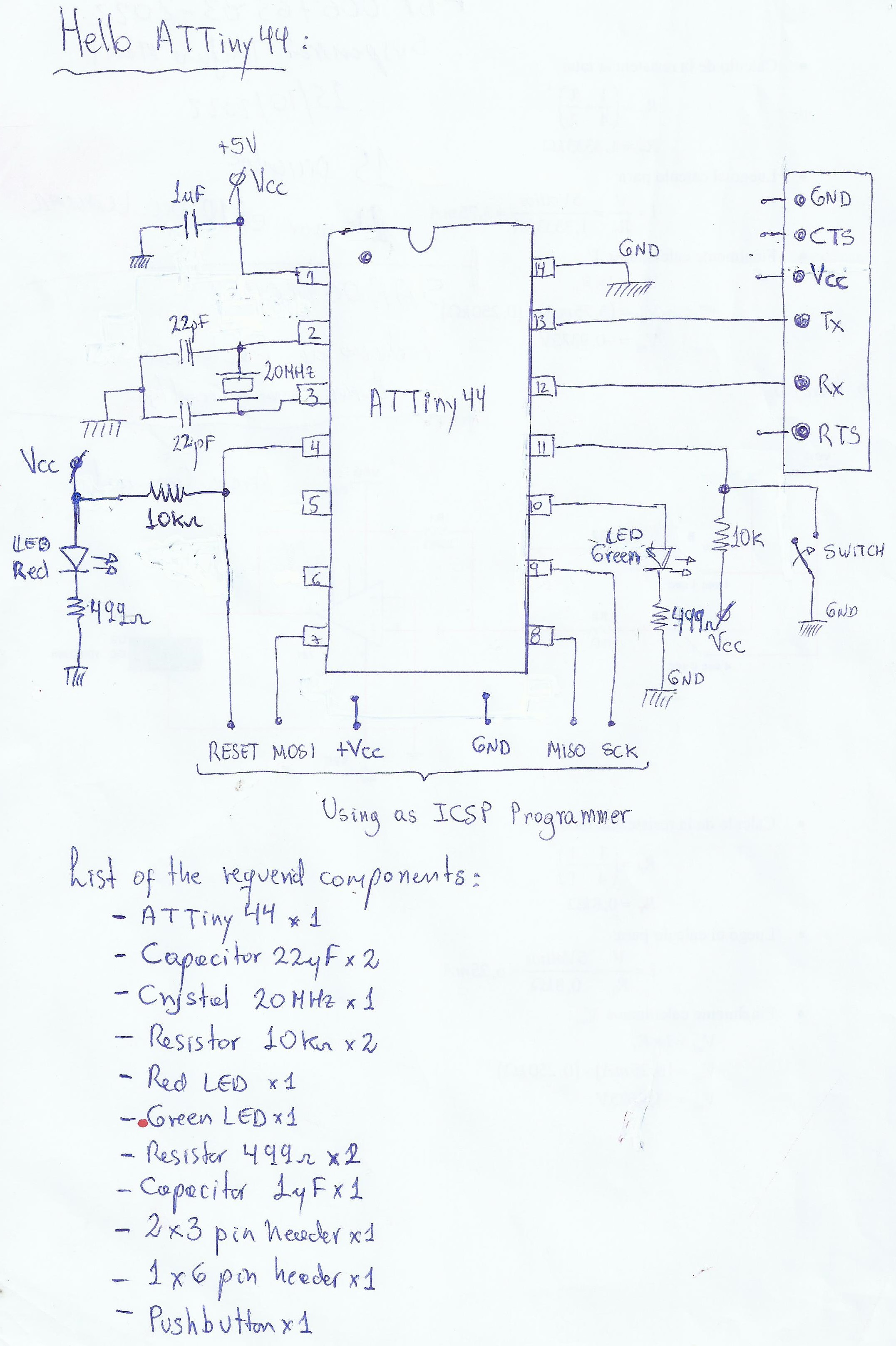
- Now I make a program “Hello ATTiny45” that by means of a pushbutton connected to PA2 (pin11) turns on a LED connected to PA3 (pin10), based on the designed PCB.
/*Hello ATTiny44A
  Pin configuration:
  ATtiny44 PA3 (pin 10)--> Green LED connected
  ATtiny44 PA2 (pin 11)--> Pushbutton connected
  Switch on and off an LED via external push button
*/

const int LED = 3;
const int BOTON = 2;
int val;
void setup() {
  pinMode(LED, OUTPUT);
  pinMode(BOTON, INPUT);
}
void loop() {
  val = digitalRead(BOTON);
  if  (val == LOW) {
    digitalWrite(LED, HIGH);
  }
  else {
    digitalWrite(LED, LOW);
  }
}
- The next step is to write the “Hello Attiny44” program to the microcontroller. If all is well, it will be successful.
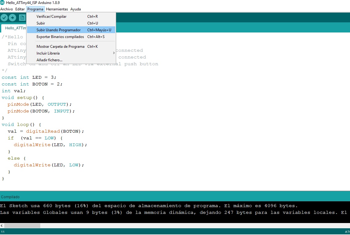
-
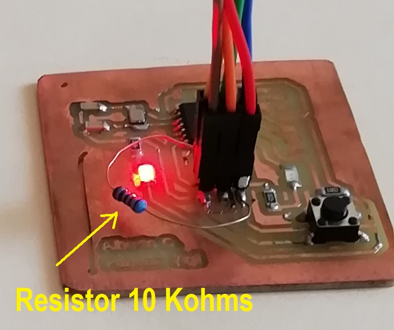
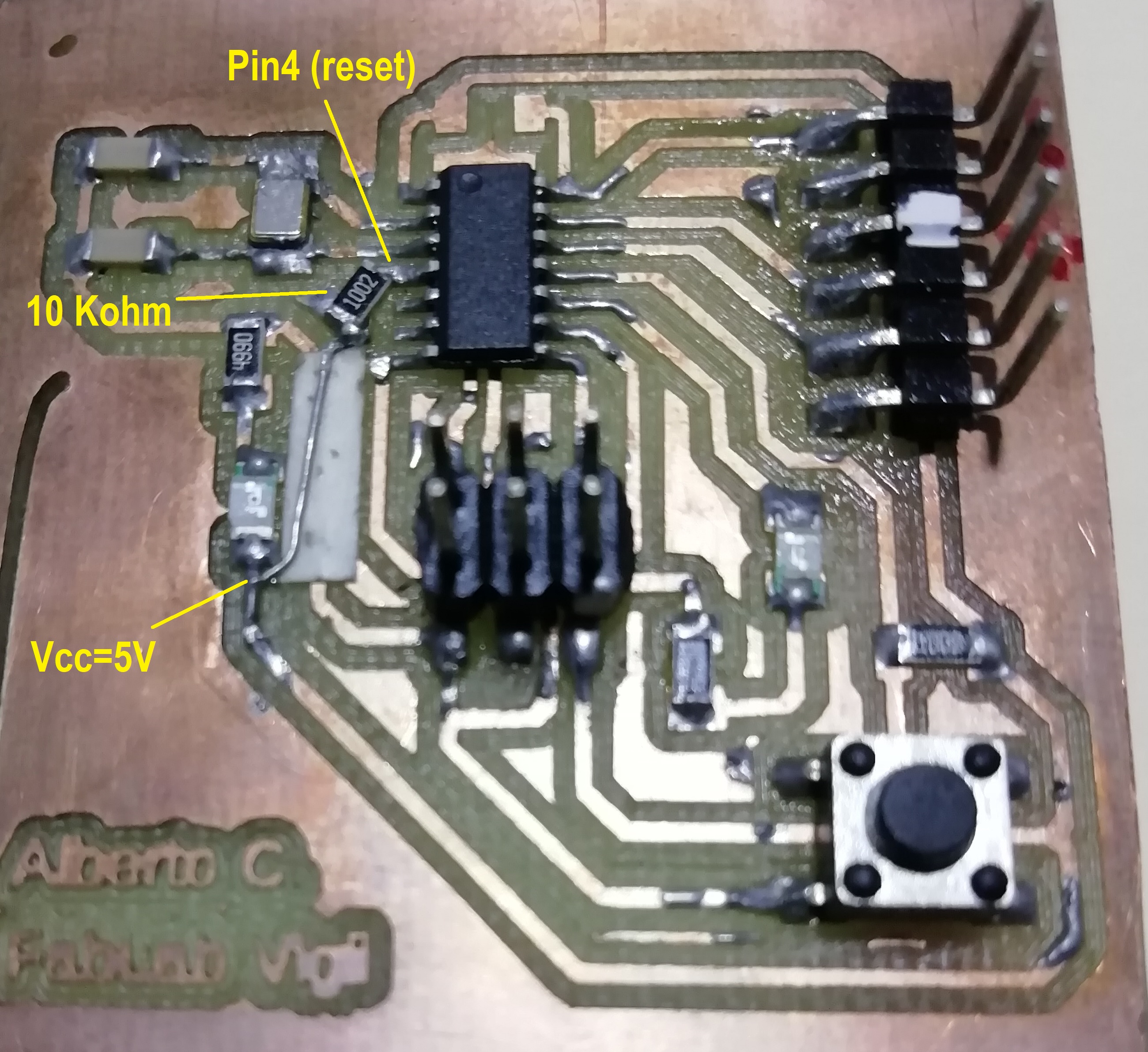
What problems did I have? At the moment of loading the program to the ATTiny, the IDE did not recognize the board, it sent me an error. I checked something that caused this error and I discovered that the Reset pin of the ATTiny did not have the 10 Kohms resistor, without the resistor the ATTiny was always in Reset so it would never load the program.
-
How did I solve it? I soldered an external 10Kohm resistor on the PCB tracks from 5V to pin4 (Reset) of the microcontroller. I transferred the program again and it worked successfully.
- Again I load the program to ATTiny44, this one is successful. I press the switch then I see that the green LED lights up. I got it and enjoyed the effort.
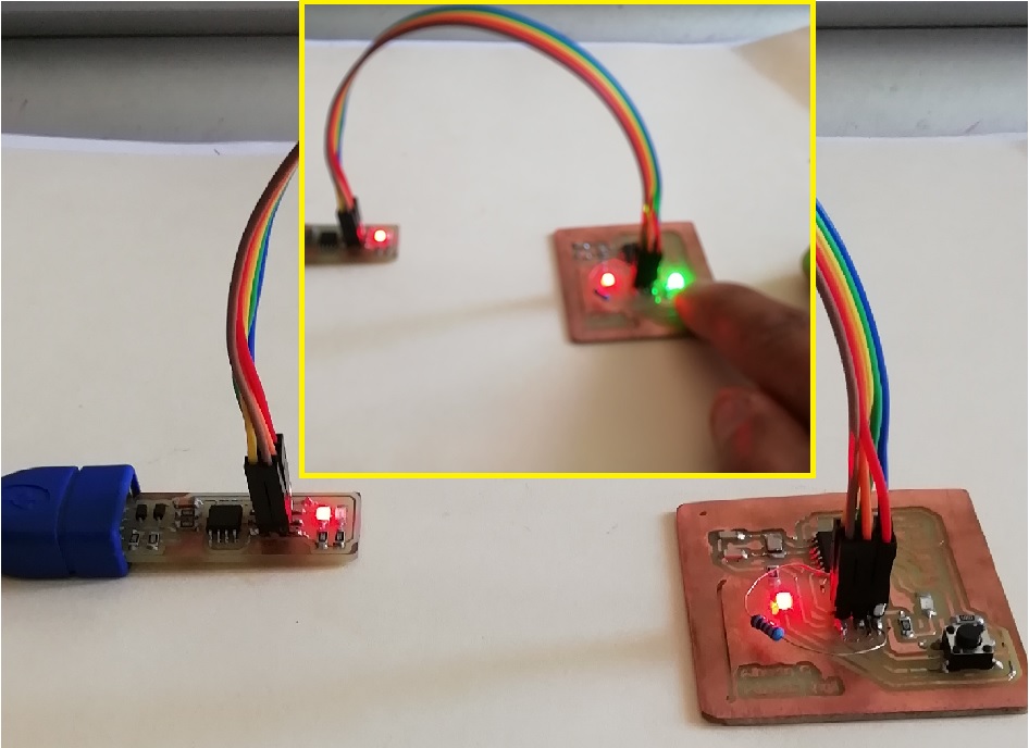
- We can see demonstration, watch this video:
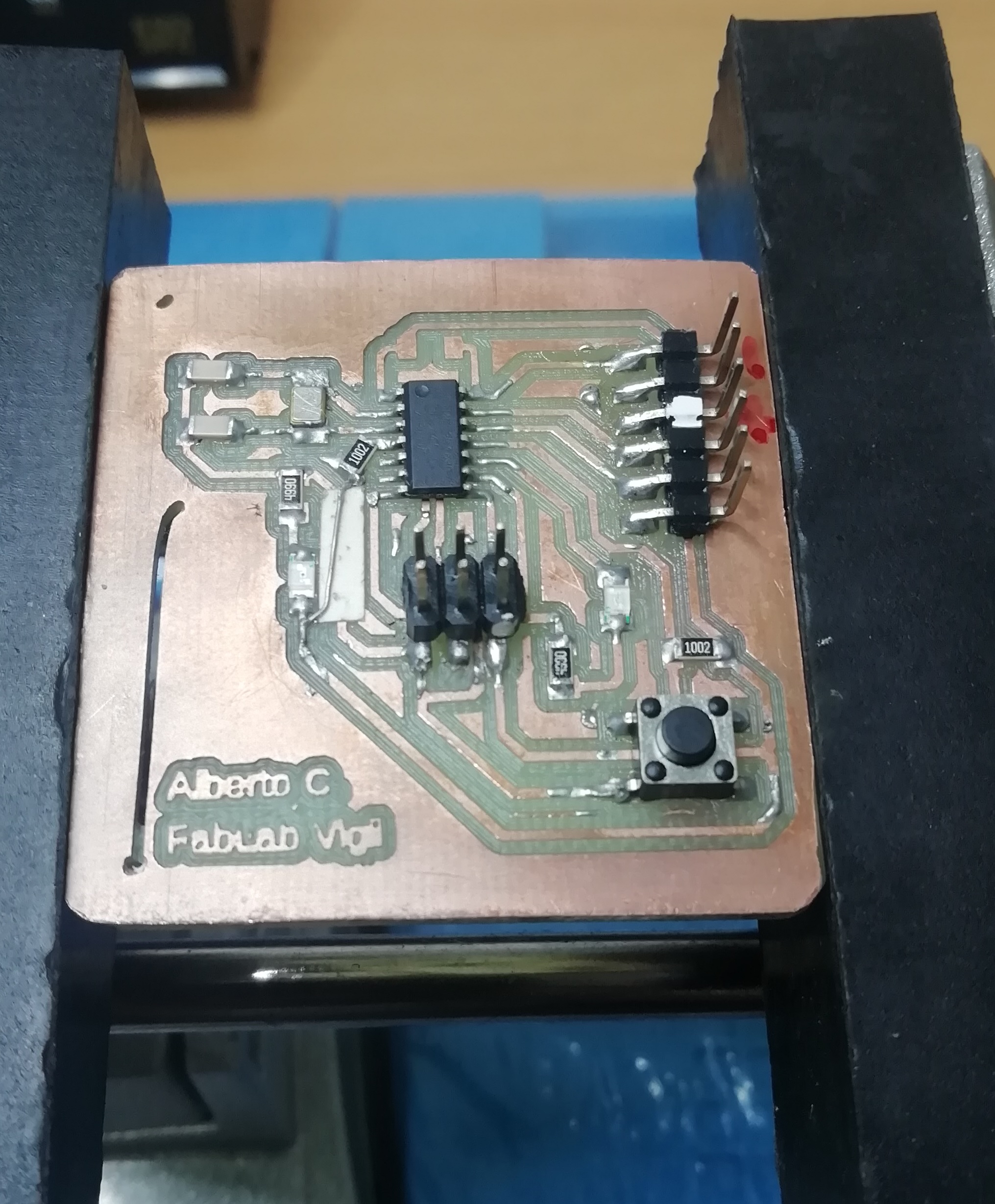
- Complementing the soldering of the SMD resistor on the PCB. Here is the result.
Simulation (Optionally):
- As it must turn on two LEDs, I must calculate the appropriate value of the resistor that limits the current, so that the LEDs do not burn out.
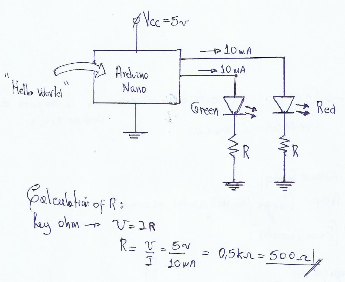
- For the simulation use Proteus 8
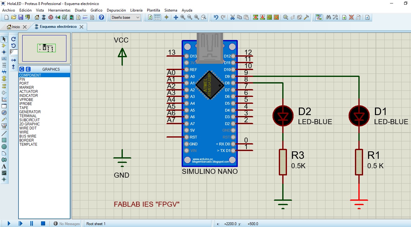
- For this case, program the arduino so that it turns on two LEDs alternately every second.
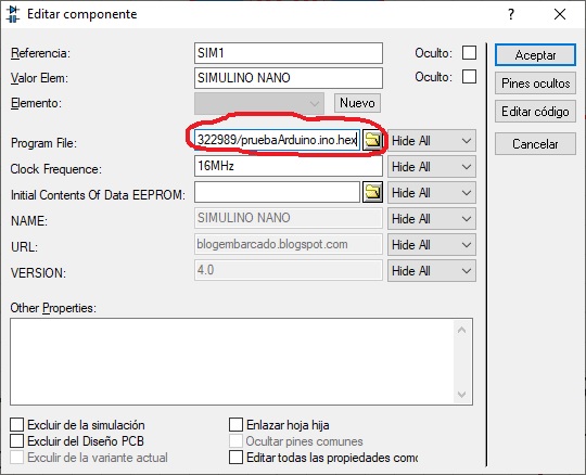
- I compile and copy the path of the hexadecimal file with extension .hex.
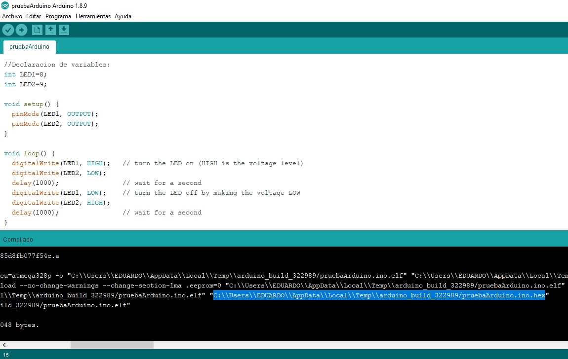
- The C code in Arduino is as follows:
Code to copy:
// Program Hello LED
// Autor: Alberto Cohaila B.
// FabLAB: IES "PFGV" - 2022.

// Declaration of variables:

int LED1=8;
int LED2=9;

void setup() {
  pinMode(LED1, OUTPUT);
  pinMode(LED2, OUTPUT);
}

void loop() {
  digitalWrite(LED1, HIGH);   // turn the LED on (HIGH is the voltage level)
  digitalWrite(LED2, LOW);
  delay(1000);                // wait for a second
  digitalWrite(LED1, LOW);    // turn the LED off by making the voltage LOW
  digitalWrite(LED2, HIGH);
  delay(1000);                // wait for a second
}
- I program the arduino nano with the hexadecimal code .hex. Then I paste the path of the .hex file and click accept.
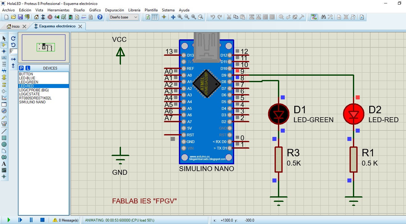
- Finally I run the simulation and see that the LED’s turn on and off alternately. Turn on the red Green for 1 sec.
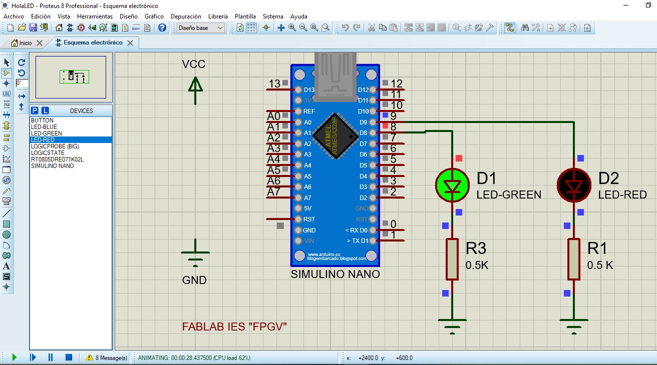
- Turn on the red LED for 1 sec.
Design Files
| Description | Files | |
|---|---|---|
| Eagle Schematic | HelloATTiny_44_2.sch | |
| Eagle Board | HelloATTiny_44_2.brd | |
| PCB Traces | echo-hello-word-Alberto-Traces.png.rml | |
| PCB outline | echo-hello-word-Alberto-Outline.png.rml | |
| Imagen Board | echo-hello-word-Alberto-Traces.png | |
| Imagen outline | echo-hello-word-Alberto-Outline.png | |
| HelloATTiny44 file | Hello_ATTiny44_ISP.ino | |
| Proteus 8.1 Simulation file | HelloLED.pdsprj |