5. Electronics production
This week I worked on:
Group assignment:
- Characterize the design rules for your in-house PCB production process: document feeds, speeds, plunge rate, depth of cut (traces and outline) and tooling.
- Document your work (in a group or individually)
- Document your work to the group work page and reflect on your individual page what you learned
Individual assignment:
- Make an in-circuit programmer that includes a microcontroller by milling and stuffing the PCB, test it to verify that it works.
Working in group:
- While Professor Niels explained the class, we captured the image of the model pattern that interested us.
- According to the linear test pattern, we search and select references on the web.
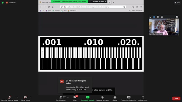
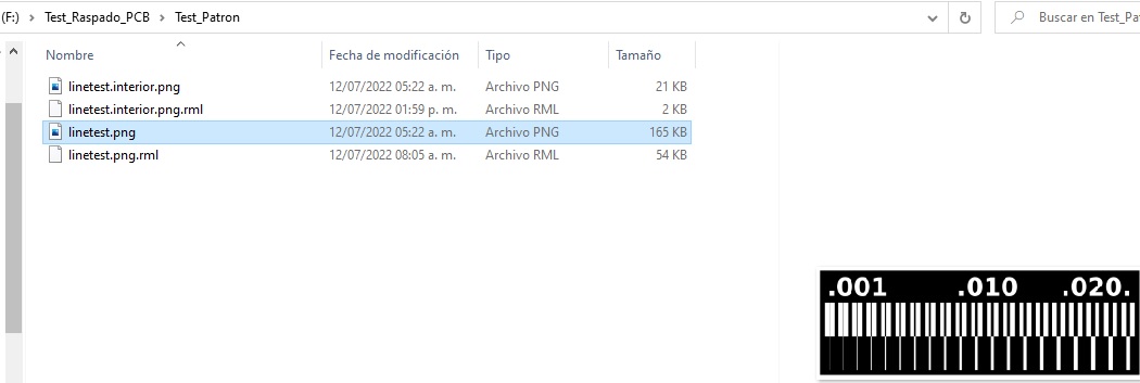
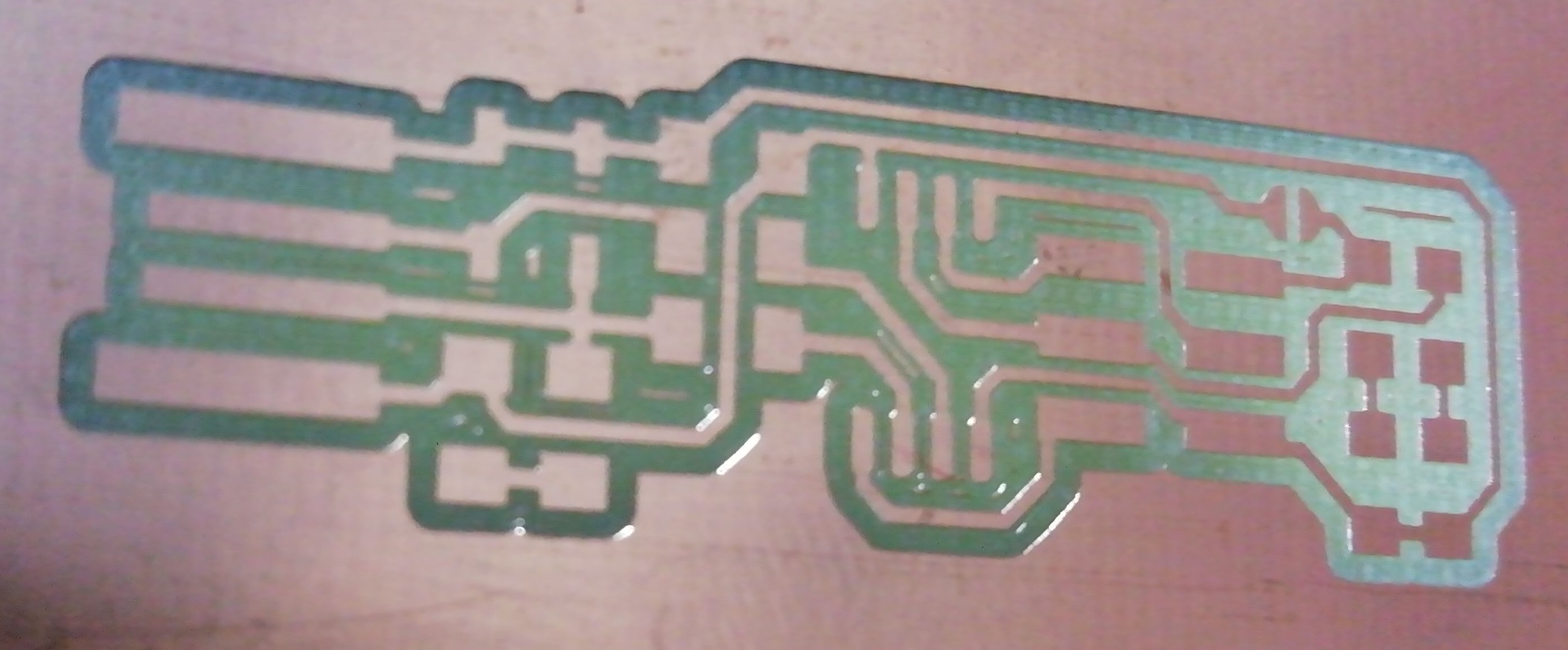
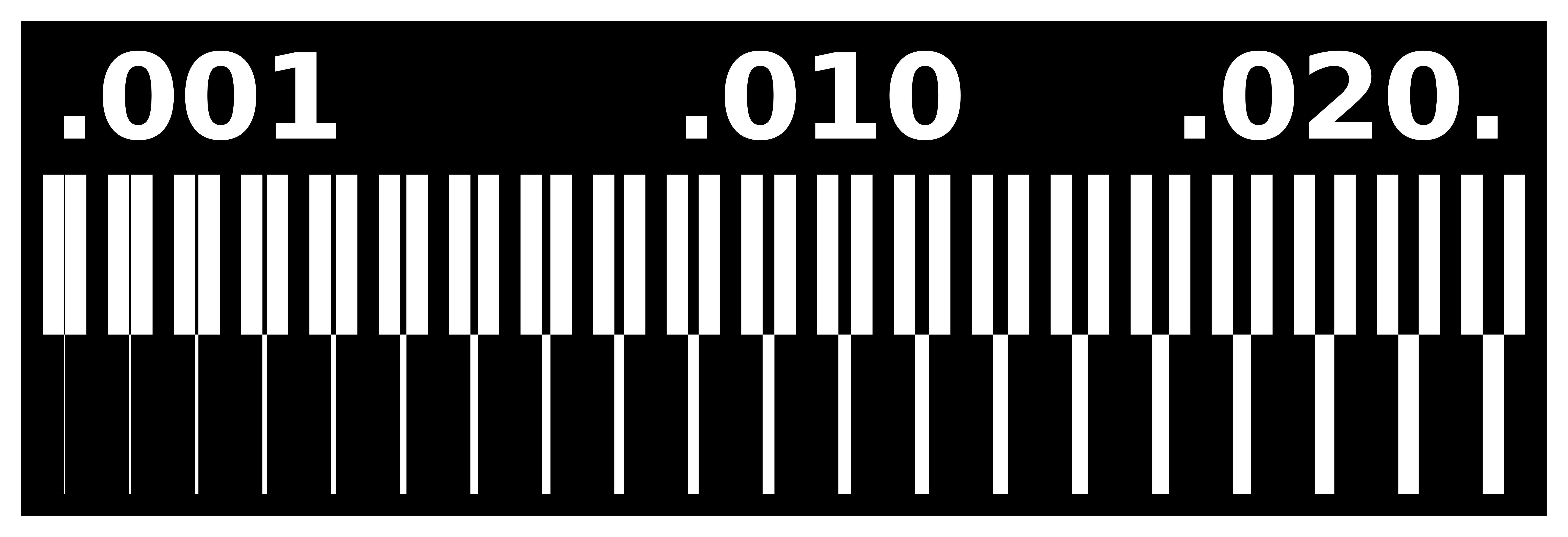
Pattern_Test.png : This is the picture of our in-house PCB production process to test the resolution of the machine.

-
For reasons of not having the Digital Manufacturing Laboratory, our work is pending to be tested on a CNC machine.
-
The exploration of the Fabmodule is pending.
Reflection:
Unfortunately, due to not having the PCB production machine, the procedures for obtaining the standard printed circuit board have not been carried out, leaving our practical knowledge without any reinforcement.
- Note: Once the teams arrived at the IES FPGV, we began to carry out the pending work as of 07-04-2022
Machine:
We have 1 Monofab machine that we have at our disposal. Let’s describe the SRM-20 in detail:

SRM Specifications:
Work area: 203 x 152 x 60mm
Loadable workpiece weight: 2kg
Operating speed: 6mm/min - 1,800mm/min
Spindle speed: 3,000 ~ 8,000rpm
Input Format : RML-1 (.rml)
Material: PCB, Modeling Wax, Chemical Wood, Foam, Acrylic
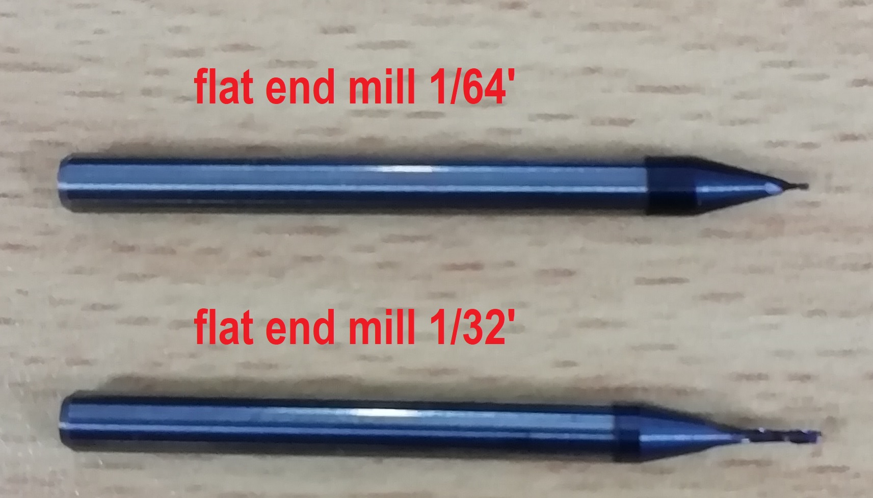
- The tools we have at our disposal are: 1/64-inch cutters for tracing (or scraping) and 1/32-inch cutters for PCB contouring.
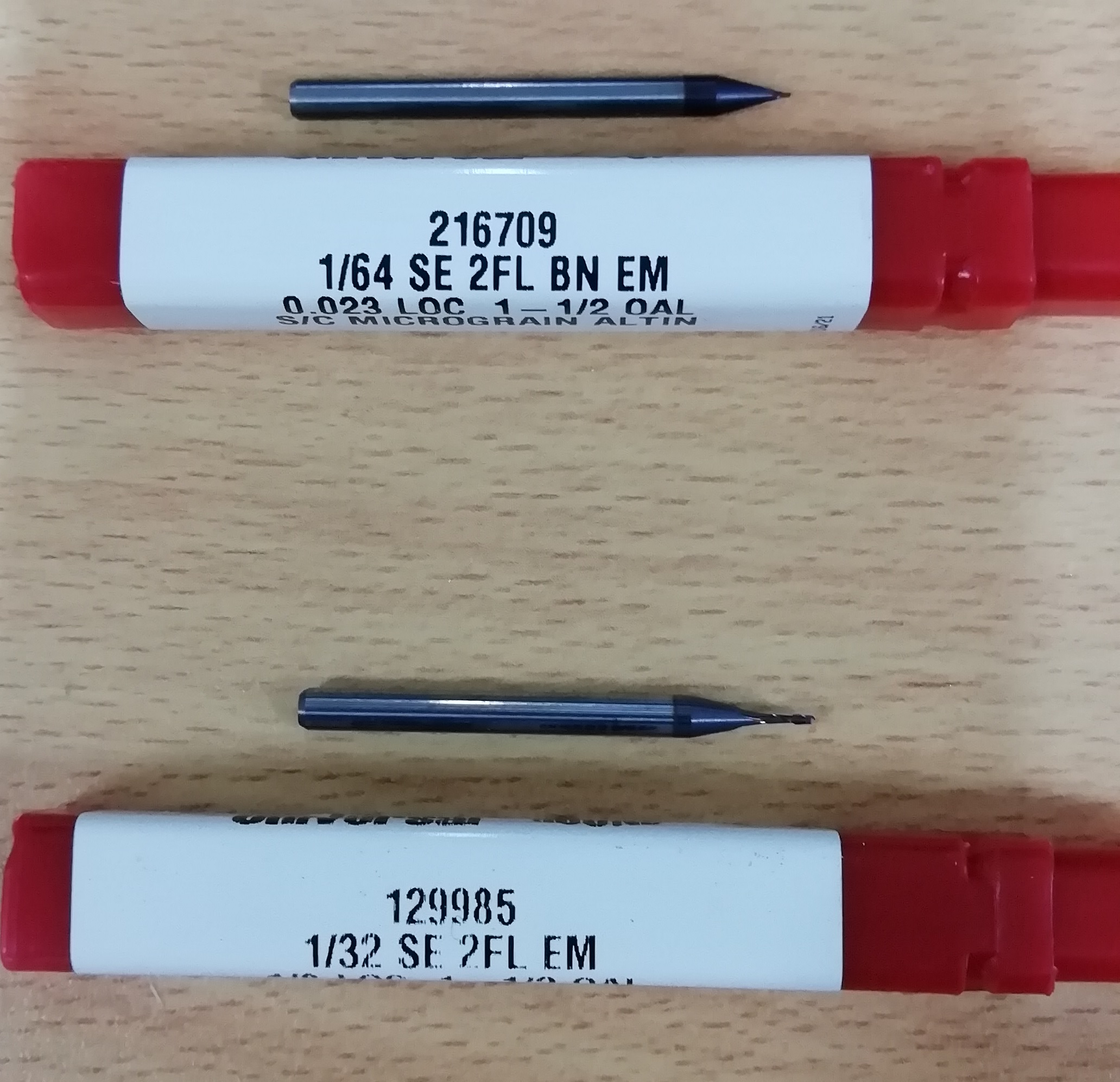
- These cutters are the most used for PCB manufacturing with the Roland SRM-20.
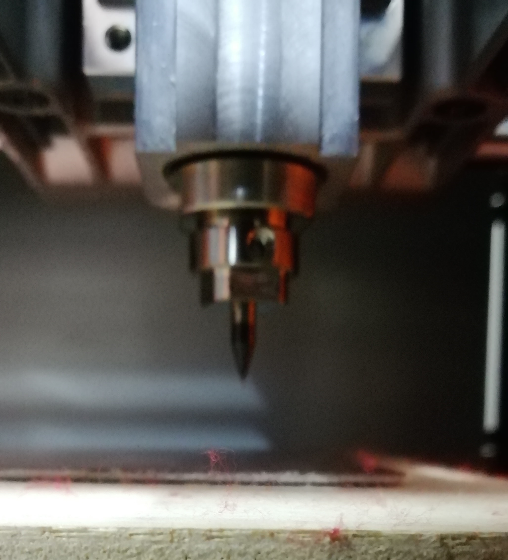
The tip of the bur should not be touched with the fingers and handled with care.
Fab Modules:
The fab modules provide a set of software tools for personal fabrication, intended for use with machines common to fab labs.
- To facilitate the work of creating the PCB, we have the fabmodules and mods to transform from pngs to .rml format that the SRM-20 uses. There are two active links:
a) https://modsproject.org
b) https://mods.cba.mit.edu
-
In our case we will use the first.
-
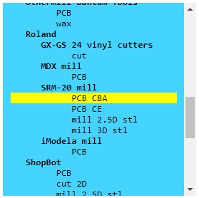
In the mod environment, just open Programs > Open Program > Machines > SRM-20 Mill > PCB CBA. In our case we are not going to network the Monofab, so we delete the WebSocket blocks. We also enable the output to download the generated .rml file
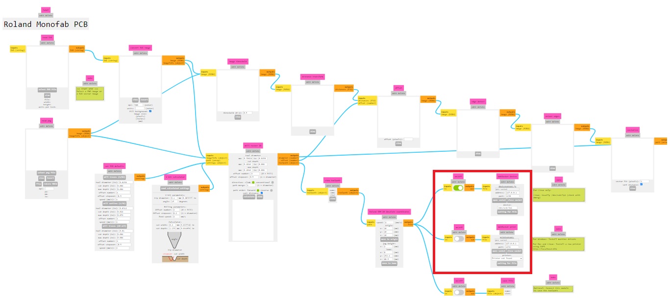
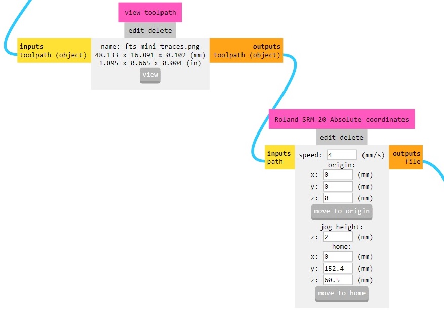
- We set the coordinates (x, y, z) to (0, 0, 0) and keep the displacement speed at 4 mm/s, jog height at 2 mm.
Resolution test
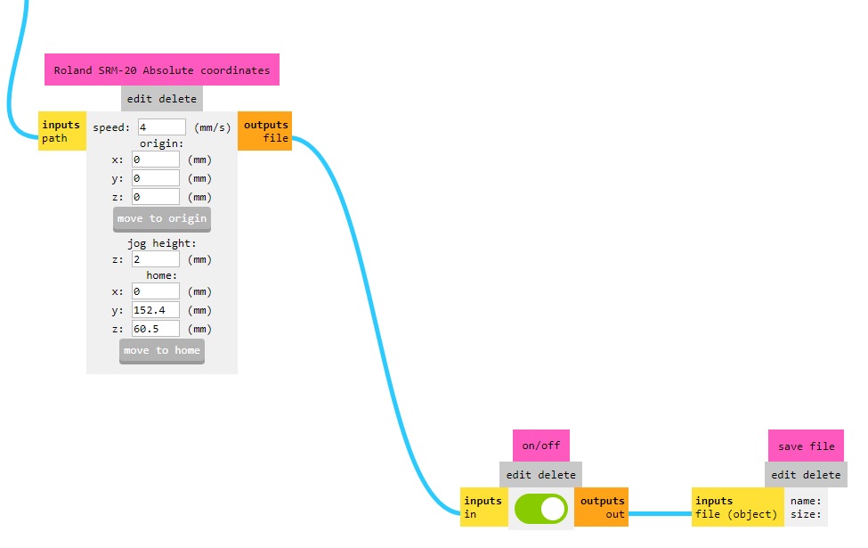
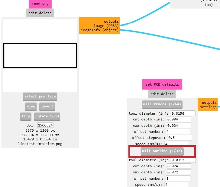
- In the read.png block we load the pattern PCB image: linetest.png
- For the mill traces we use the default settings of the mods, so we don’t have to calculate speeds and depths because they have worked perfectly.
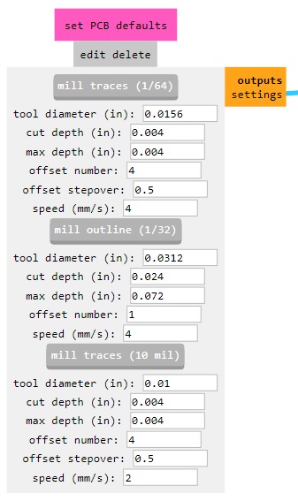
- We keep the speed at 2 mm/s and the displacement height of the milling cutter in the air at 2 mm.

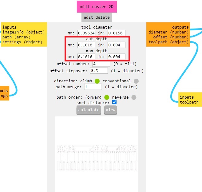
- The milling raster 2D block then calculates the cut depth, which defaults to 0.1016mm and the number of passes is 4.
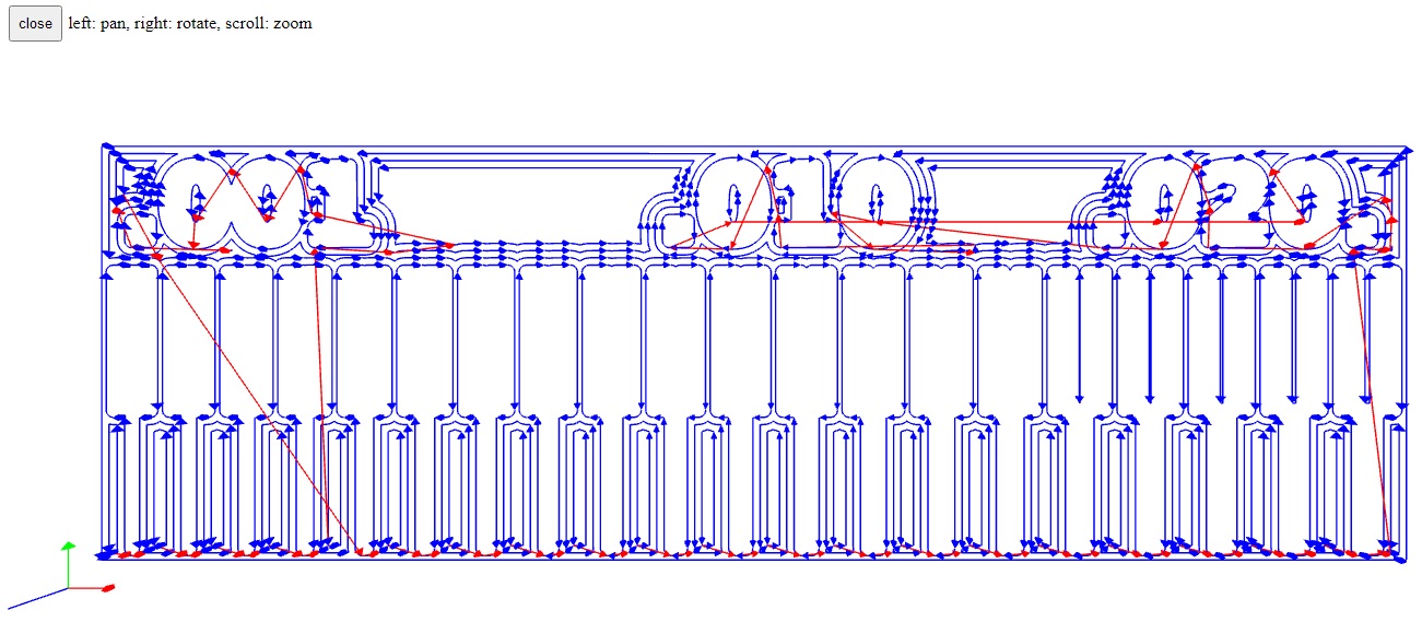
- Pressing calculate generates the .rml format that is downloaded to the computer and gives us a perspective of the pieces of the milling machine on the PCB.
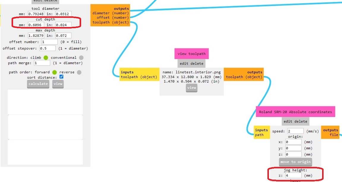
- Similarly for the PCB outline, we load the file: linetest.interior.png in the Mods. For this case we have considered a speed of 2 mm/s and a jog height of 4 mm. The depth of cut is left at 0.6096 mm.
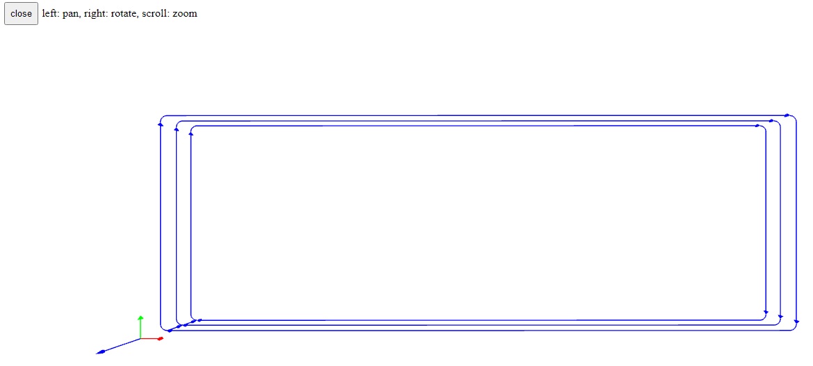
- Finally we got the two .rml’s files to perform the test. We now proceed to use the Roland SMR-20.
Testing the Monofab with the tolerance test:
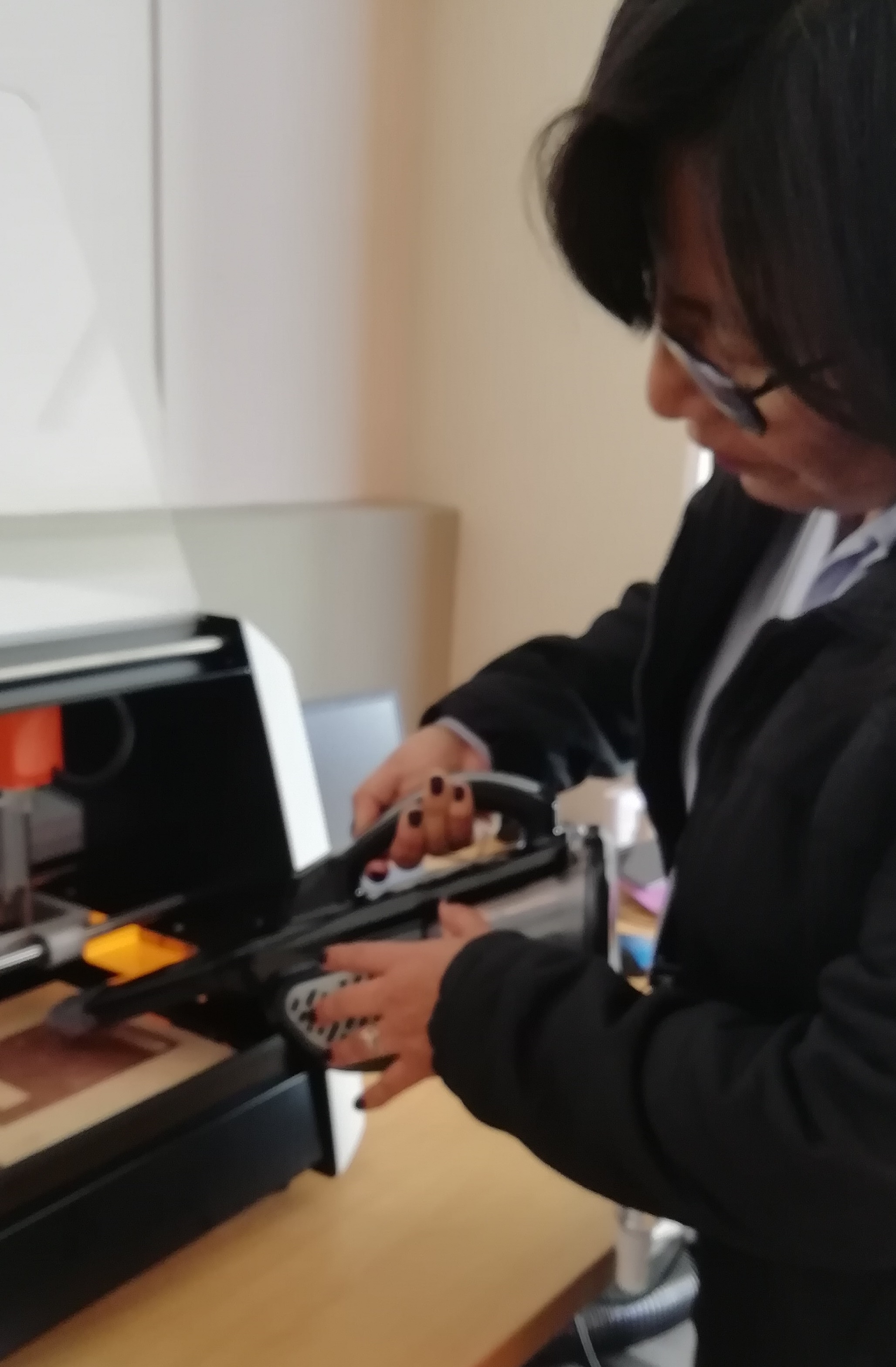
- Calibrating the initial position of work
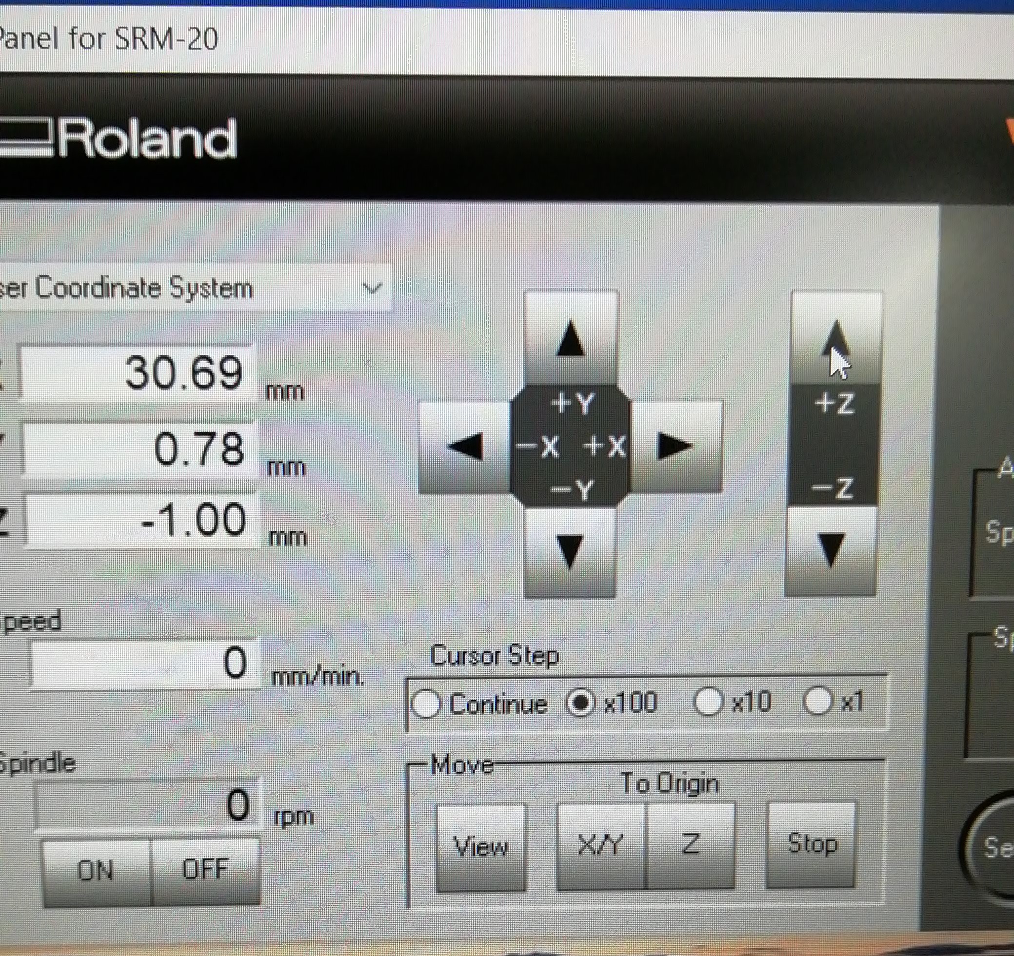
- We lower the tip of the cutter holder (Z) to the bottom. Then with the hexagonal tool we loosen and make the dam fall until it touches the PCB. We move up two positions to steps x100. Then we return to adjust the strawberry. In the Vpanel we adjust the positions of X=Y=Z=0. We load the .rml file and the cutting process begins.
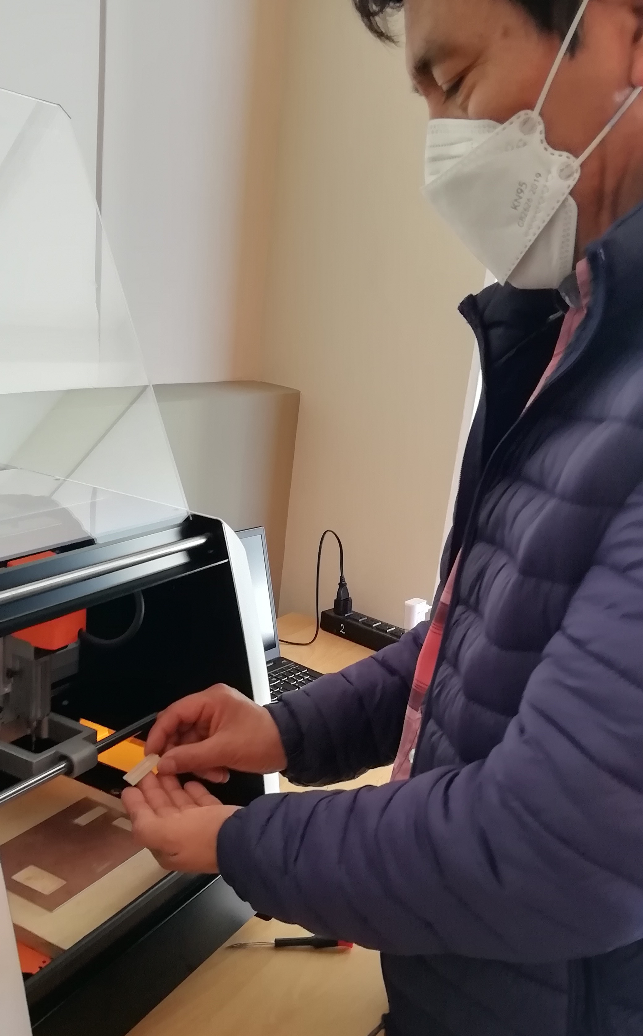
- Mill outline process.
- We carry out a cleaning of the detached chip.
- With a small flathead screwdriver, we remove the PCB pattern.

- We remove the PCB pattern.
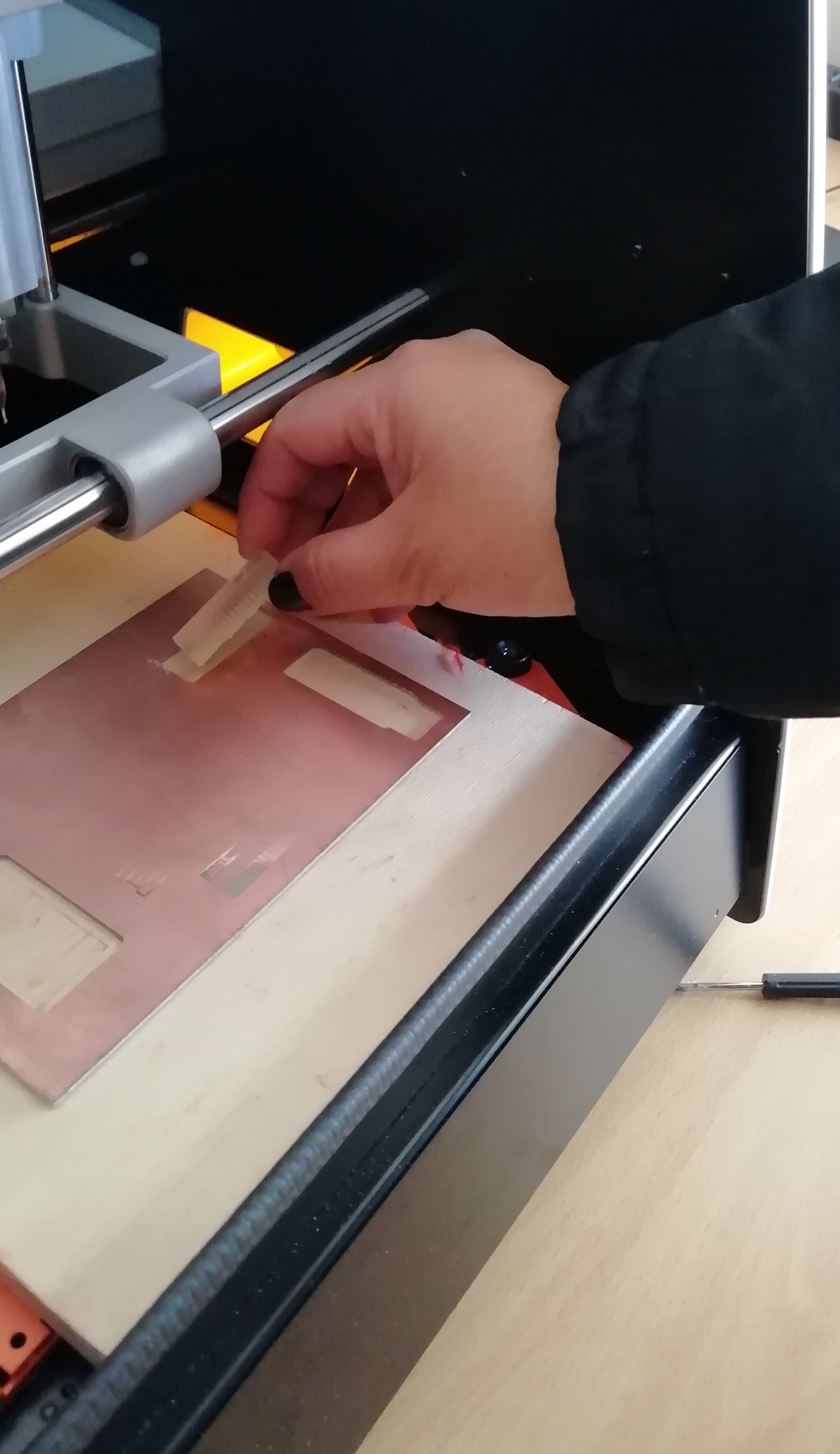
- And we have it ready :)
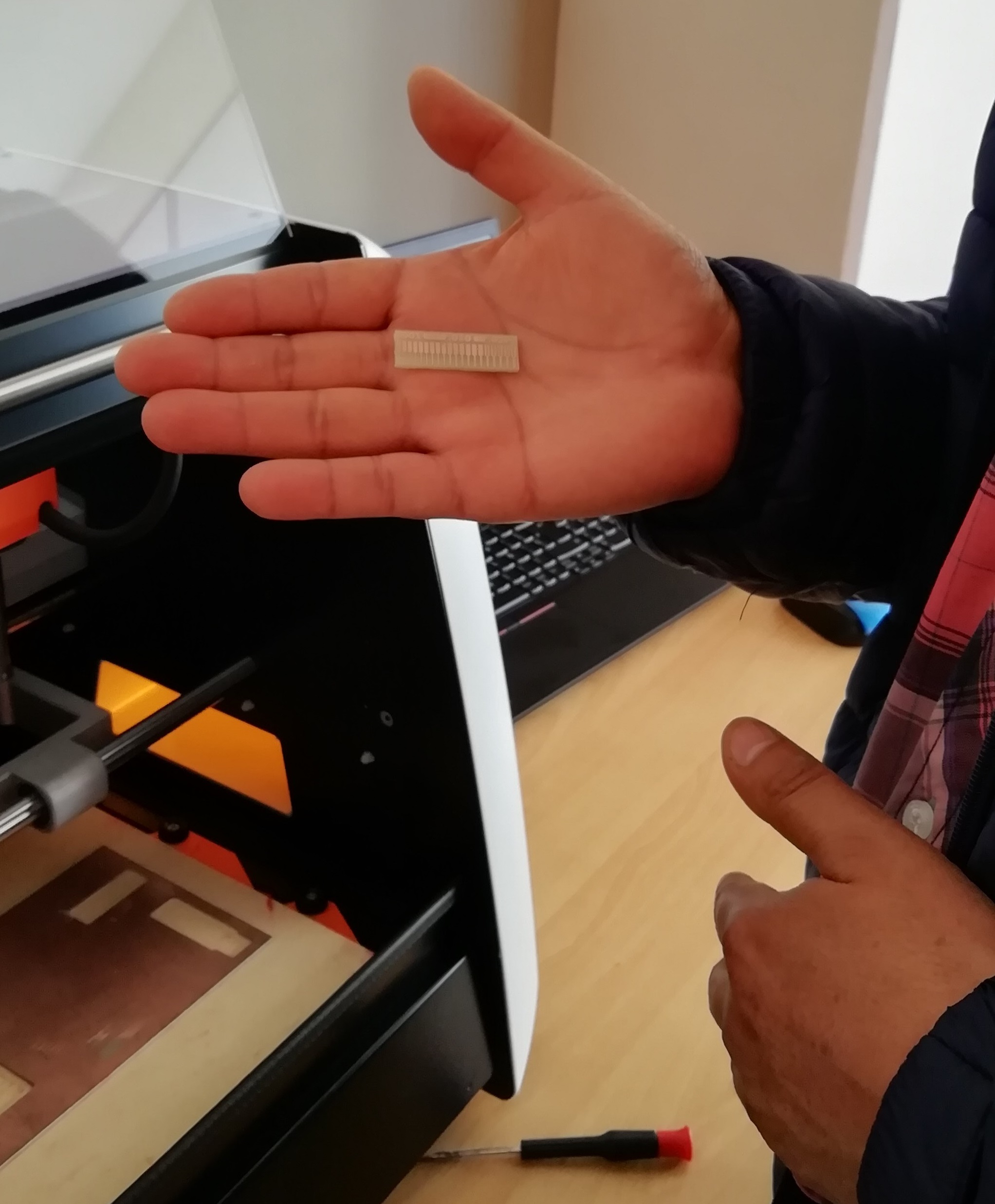
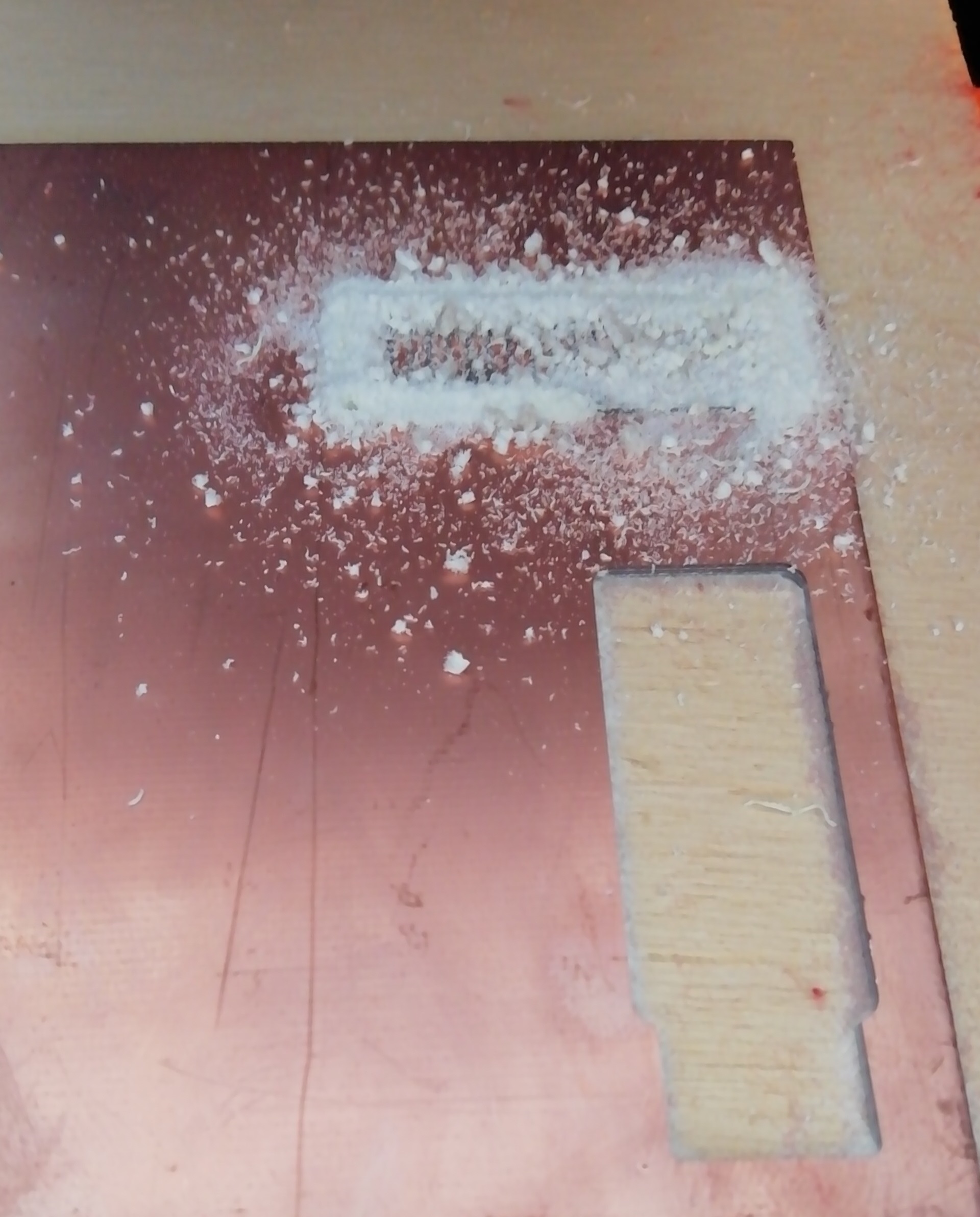
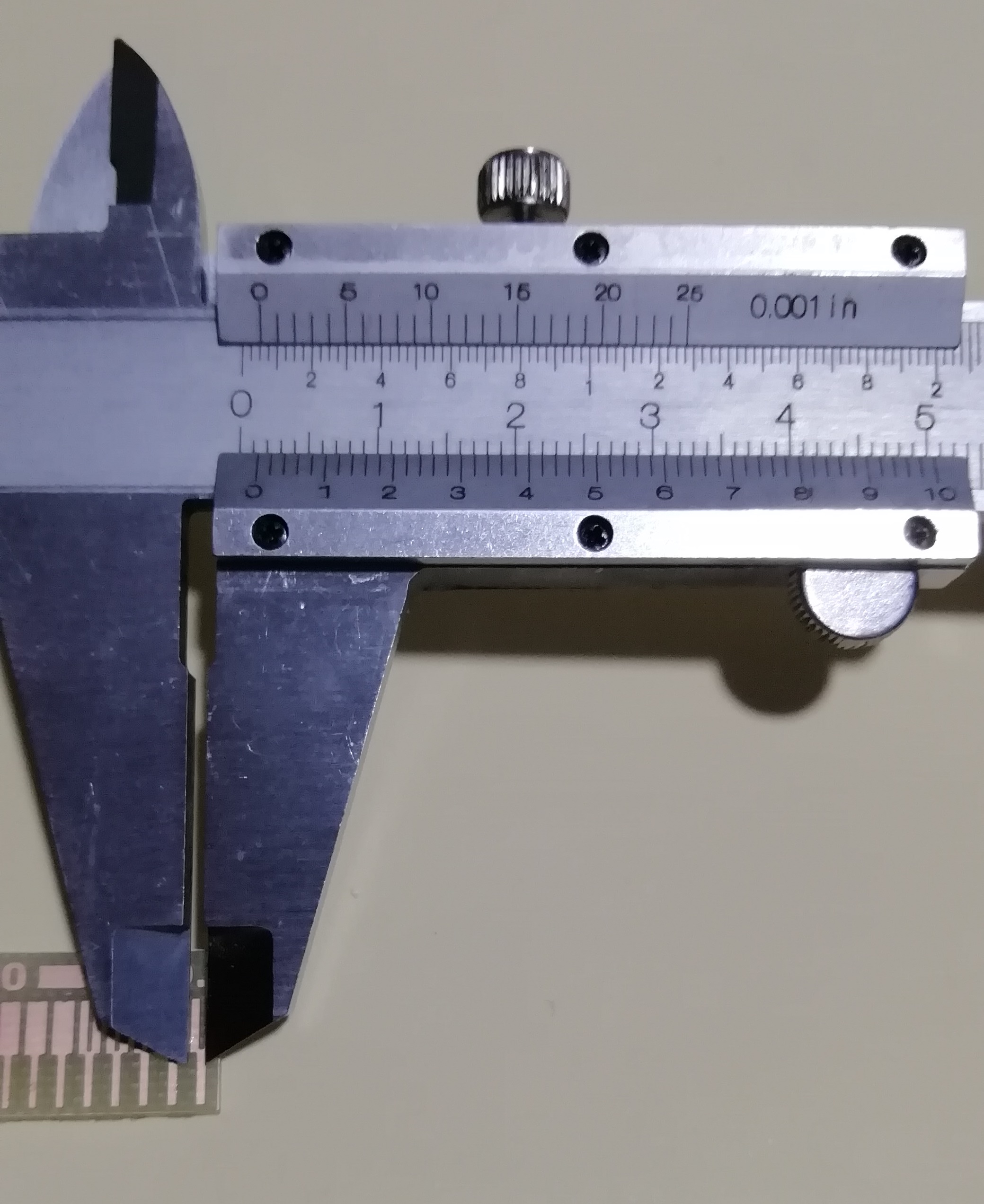
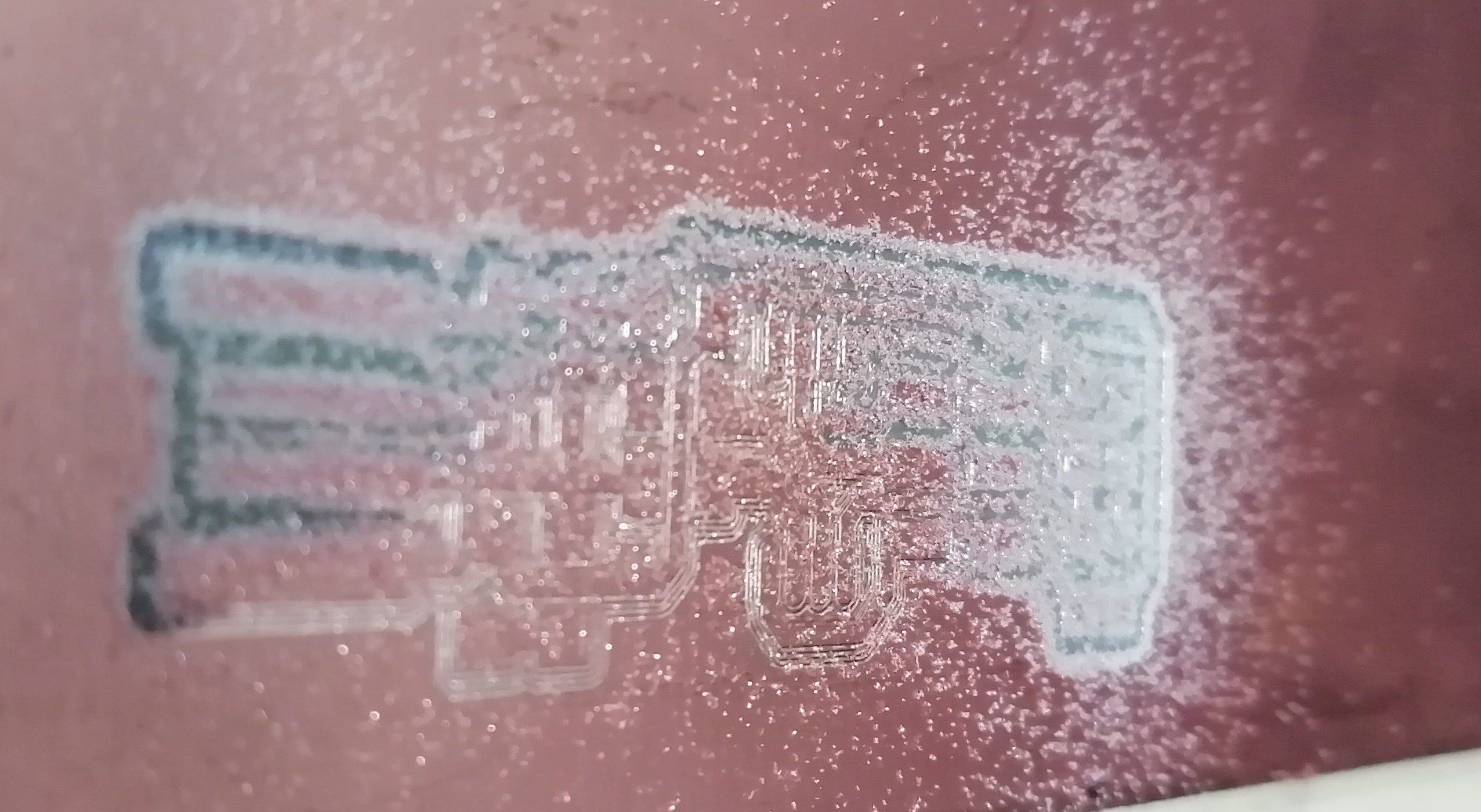
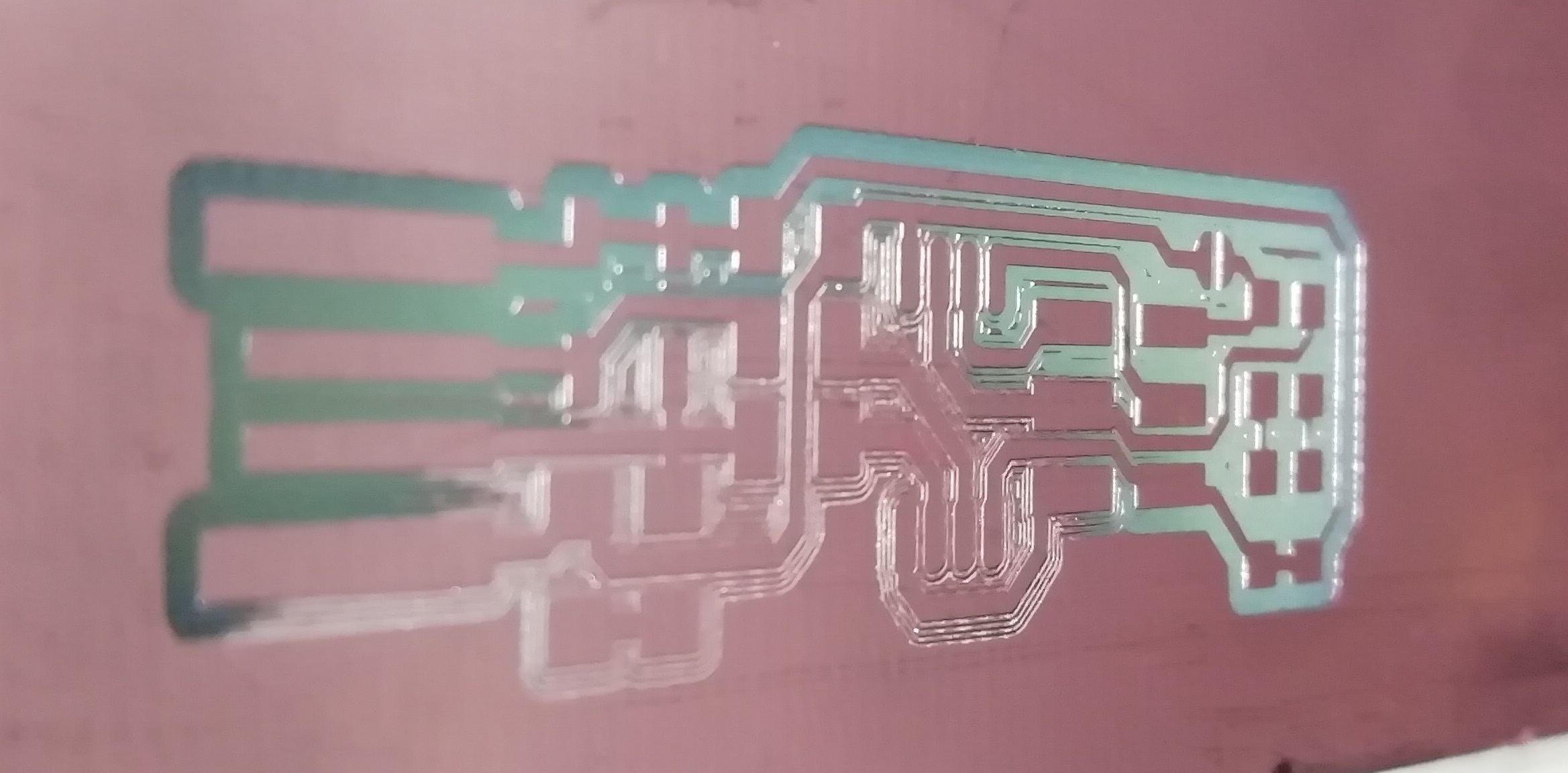
- Finally, here we have the test result:
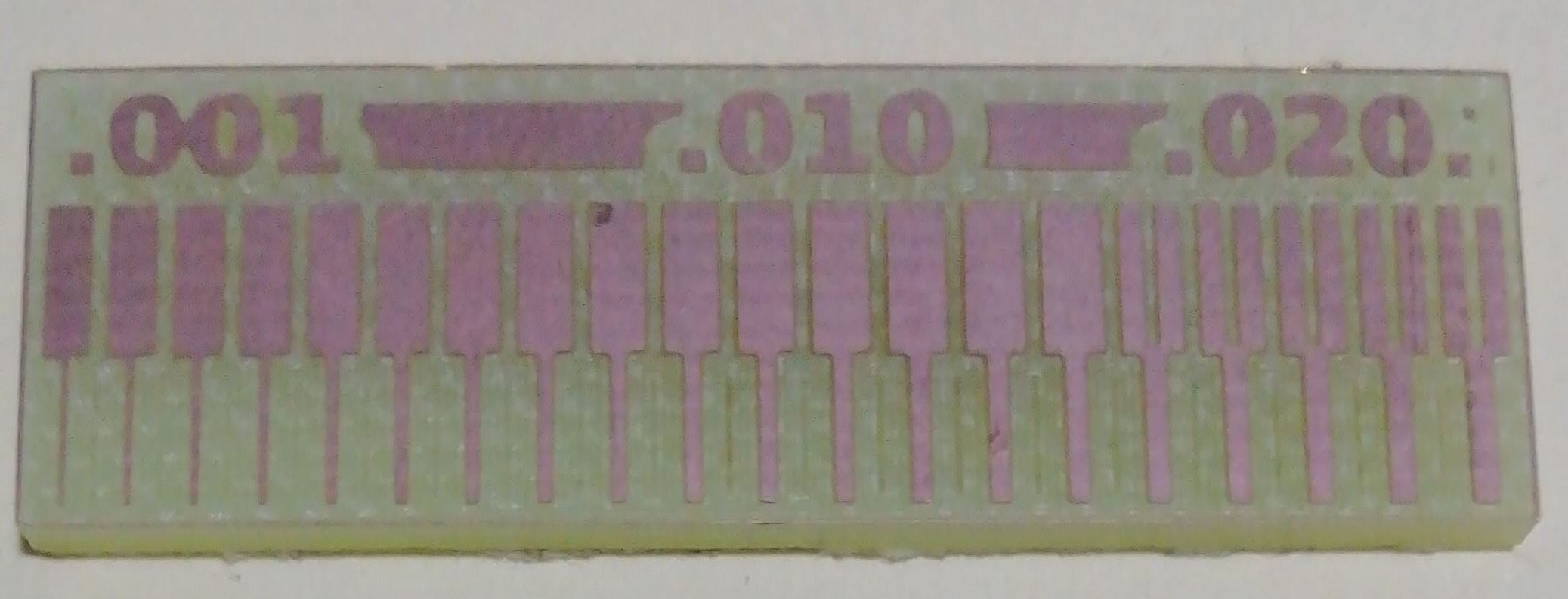
- We check the thickness of the track which is 1.38 mm.
What is learned?
-
This week we learned how to use the Monofab SRM-20, we also better understood the milling process through the design rules of the PCB production process.
-
Seeing is not the same as doing it yourself. By not having a local instructor and with the teachings of our Arequipa instructor, we were able to discover the milling process and solve the problems that arose.
-
The test pattern, being our first PCB that we made, we saw that it came out excellent. One of the factors is that since both the milling cutters and the Monofab are new, their layout resolution is 100%.
-
We are happy and eager to complete the other assignments.
Working individually: Building the FabTinyISP
There are several programming boards for mill traces. The most common in the FabAcademy are:
-
I decided to make the ISP type programmer (AVR) in the Attiny85 version made by Brian, because it is very well oriented in his document and it is easier for me.
-
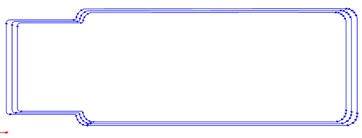
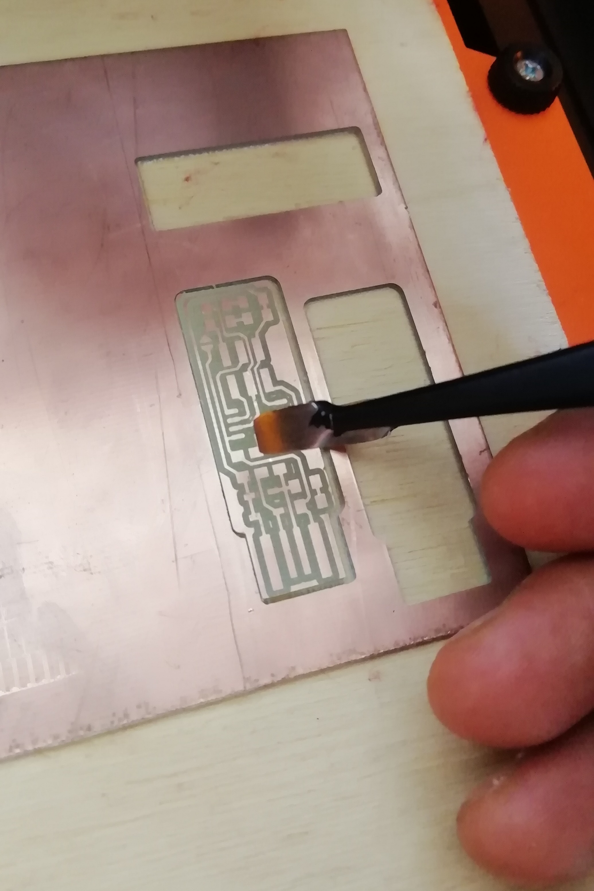
This is the image of the PCB to build (fts_mini_traces.png , fts_mini_cut.png)
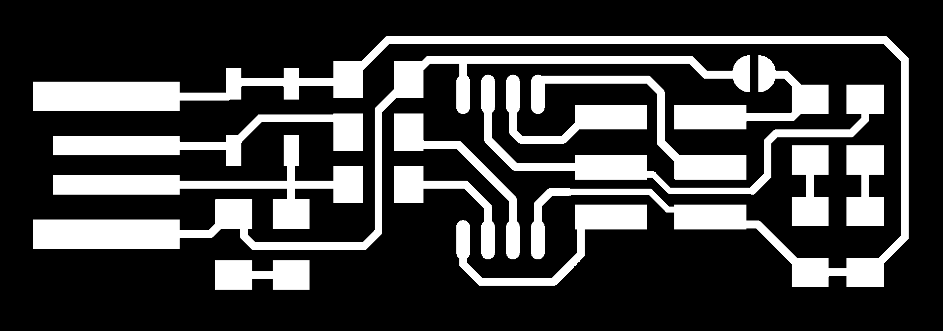 Mill traces
 Mill outlines
 - I load the file fts_mini_traces.png in the Fabmodules. The traces will be milled with a 1/64”
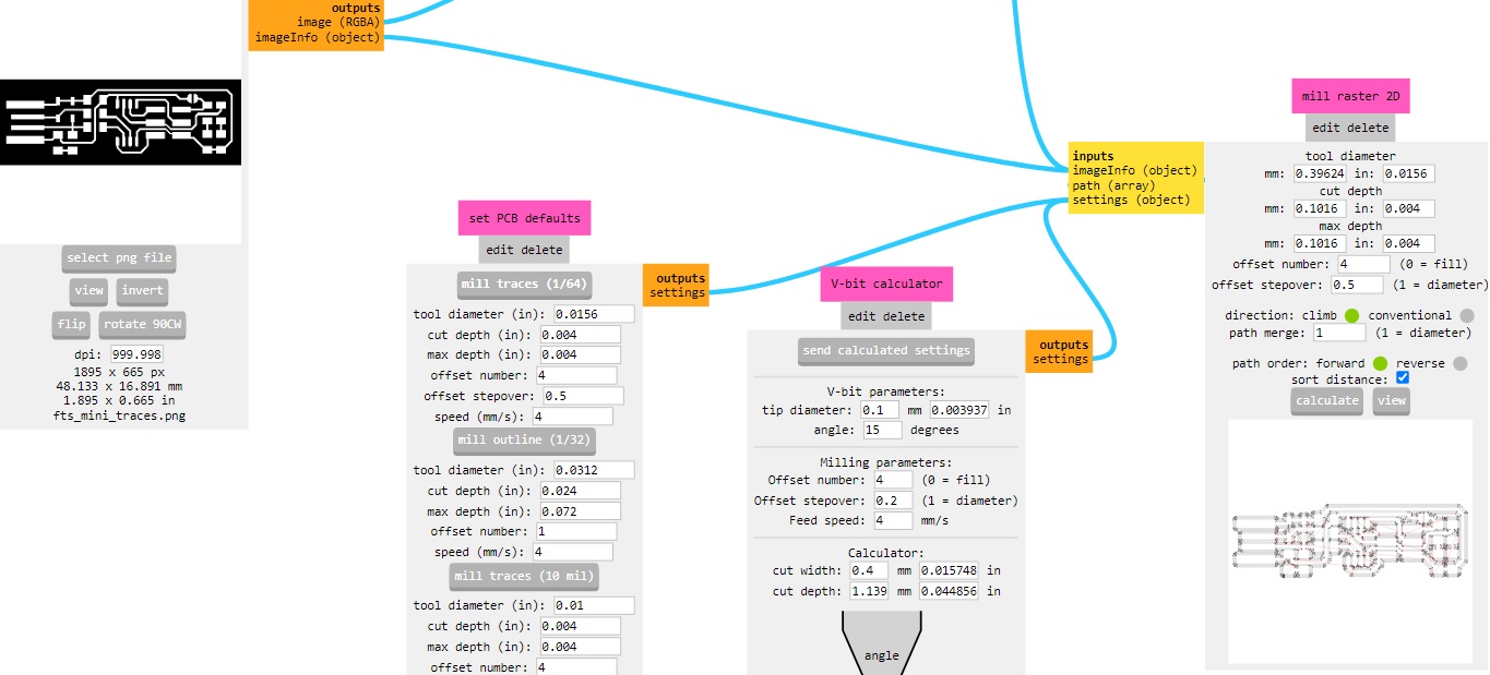
- We set the coordinates to (0,0,0) keeping the speed at 4 mm/s and jog height at 2 mm.
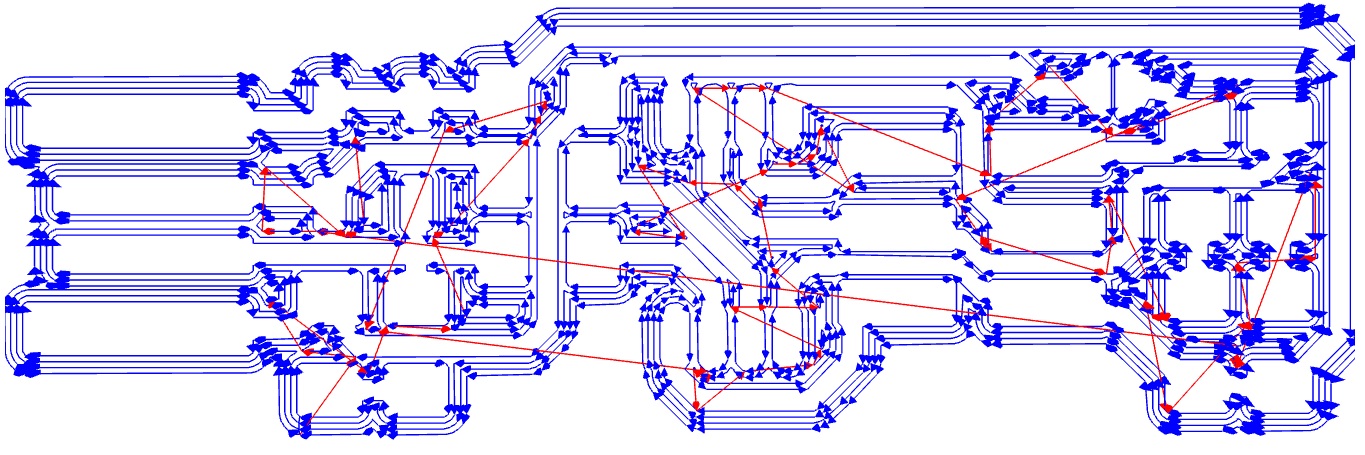
- Then I clicked ‘calculate’ to generate the trajectories and saved the .rml file
- For the contour, exactly the same steps are followed, the only difference is the process in which it is chosen as the PCB contour 1/32” this is with reference to the milling bit size.
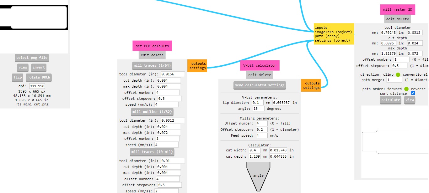
- We set the coordinates to (0,0,0) reduce the speed to 2mm/s and increase the jog height by 4mm.
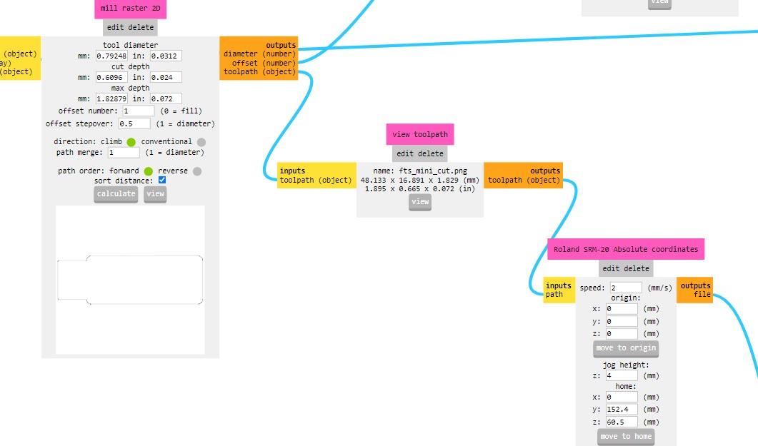
- Finally, clicked ‘calculate’ to generate the trajectories and saved the .rml file. It is now ready to be used with the machine.
Cutting the PCB
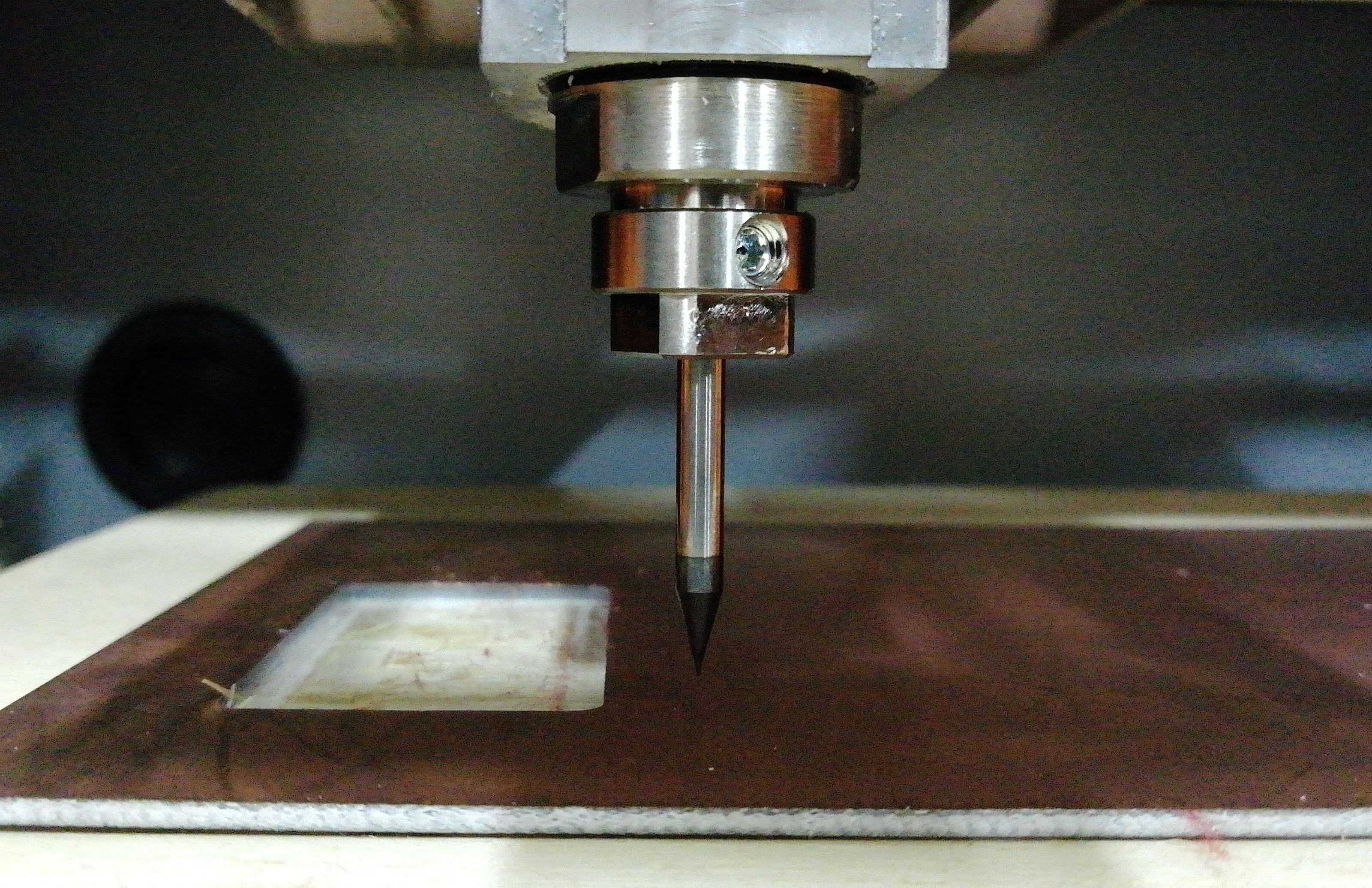
- In the Rolland machine I must position the tip of the cutter with the surface of the PCB. For this I lower the Z limit, then I go up steps x100. It is there that I release the strawberry so that it touches the PCB.
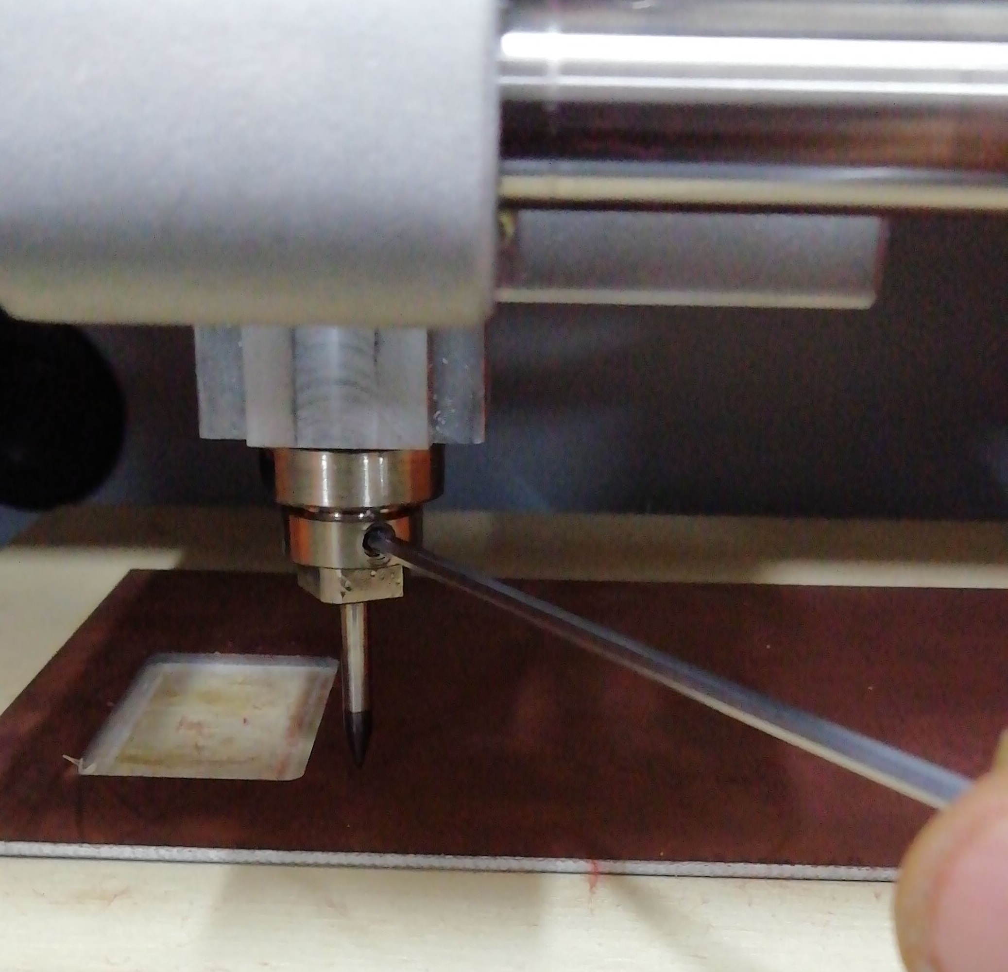
- Now the reference is at (0,0,0) from there it will start milling.
- The cutting process is fast, around 3 min.The cutter lowers 3 times to cut to the bottom of the PCB.
- I could see that one side of the design was scratched off. This occurs because the sacrificial base has a slight incline that is invisible to the eye.
-
So as not to spoil the design. I decided to lower the Z by 0.03mm so it would scrape deeper.
-
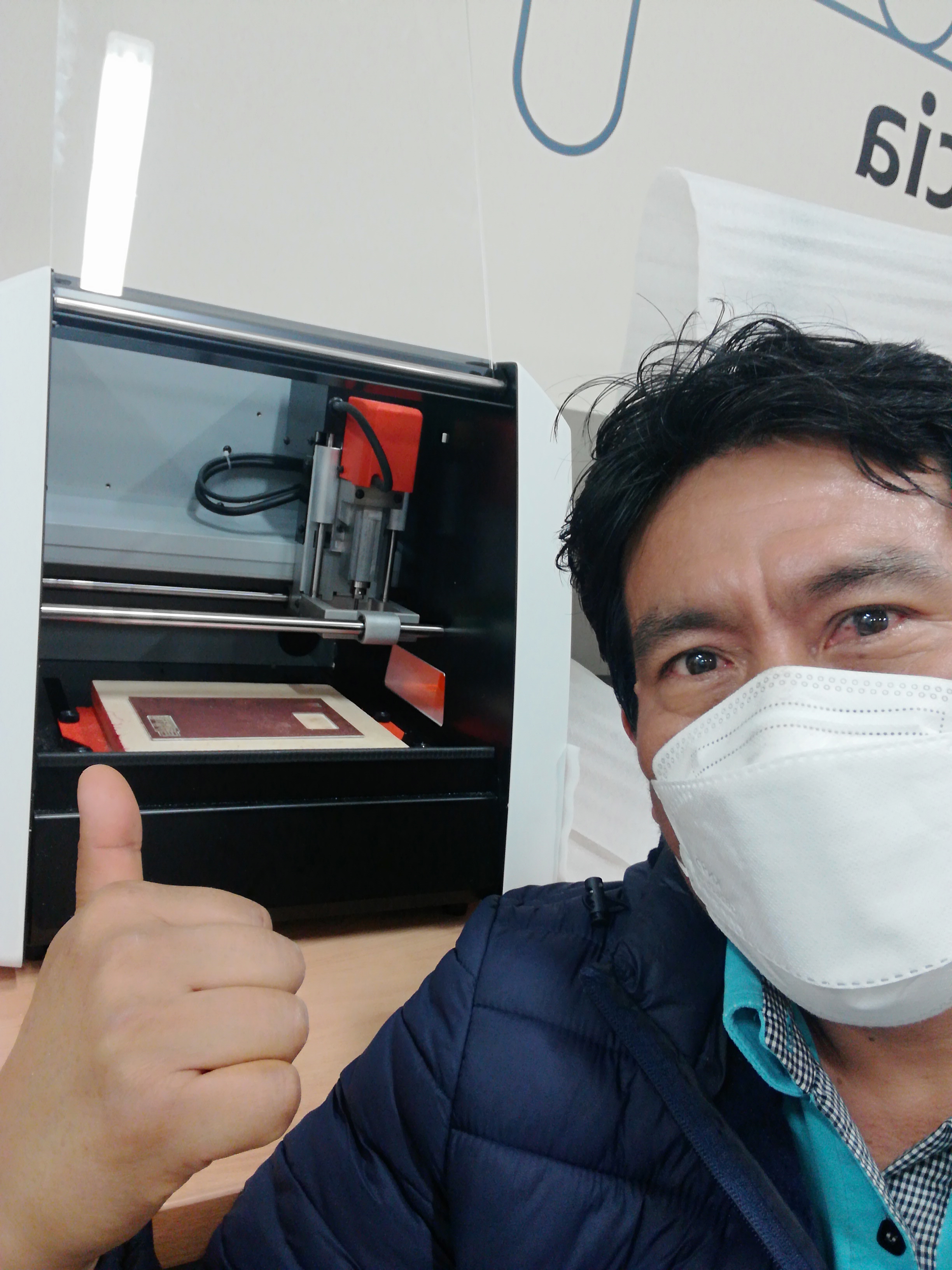
This is how the PCB looks. They have a good finish for being the first time I use the Roland. I conclude that it helped a lot to be both the machine and the new bits.
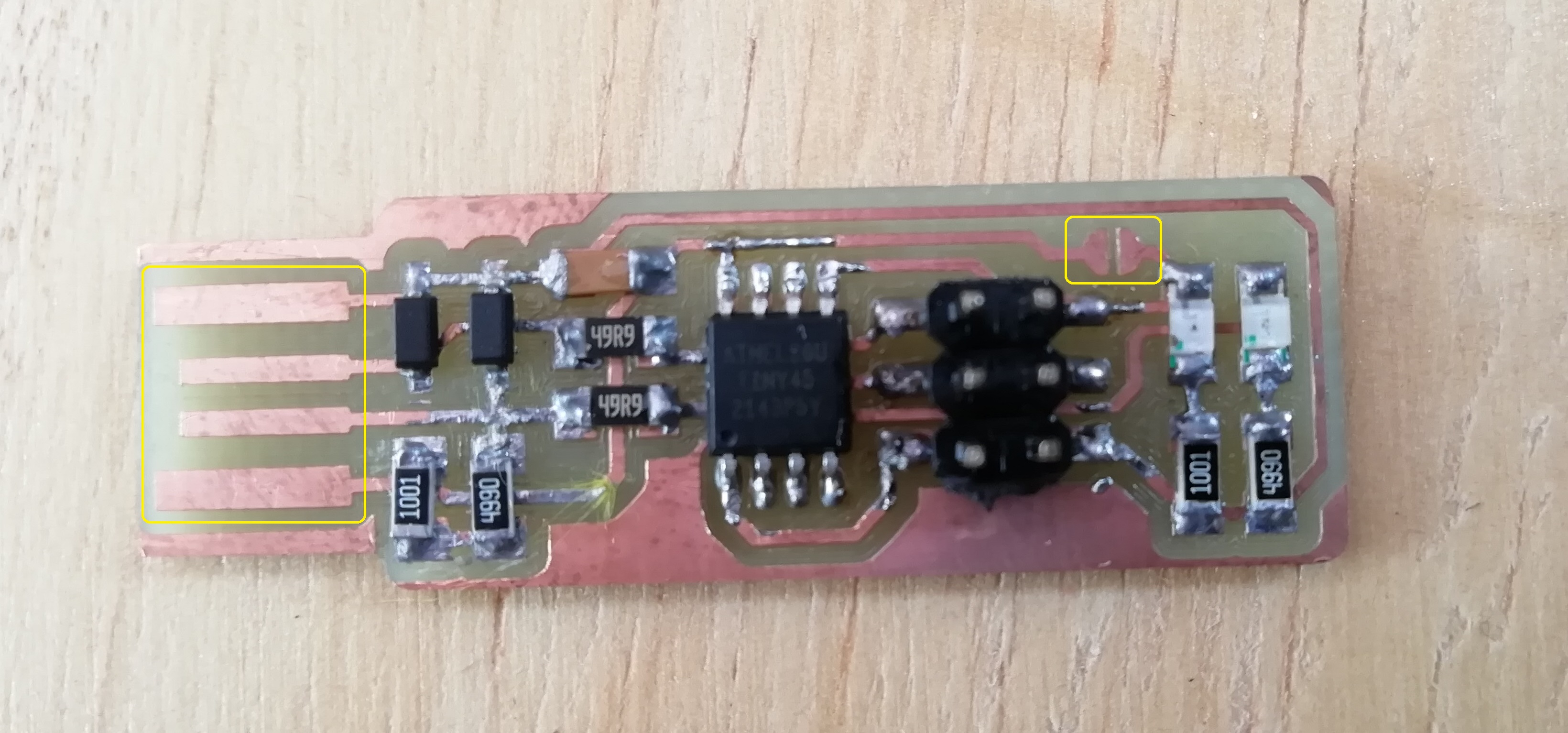
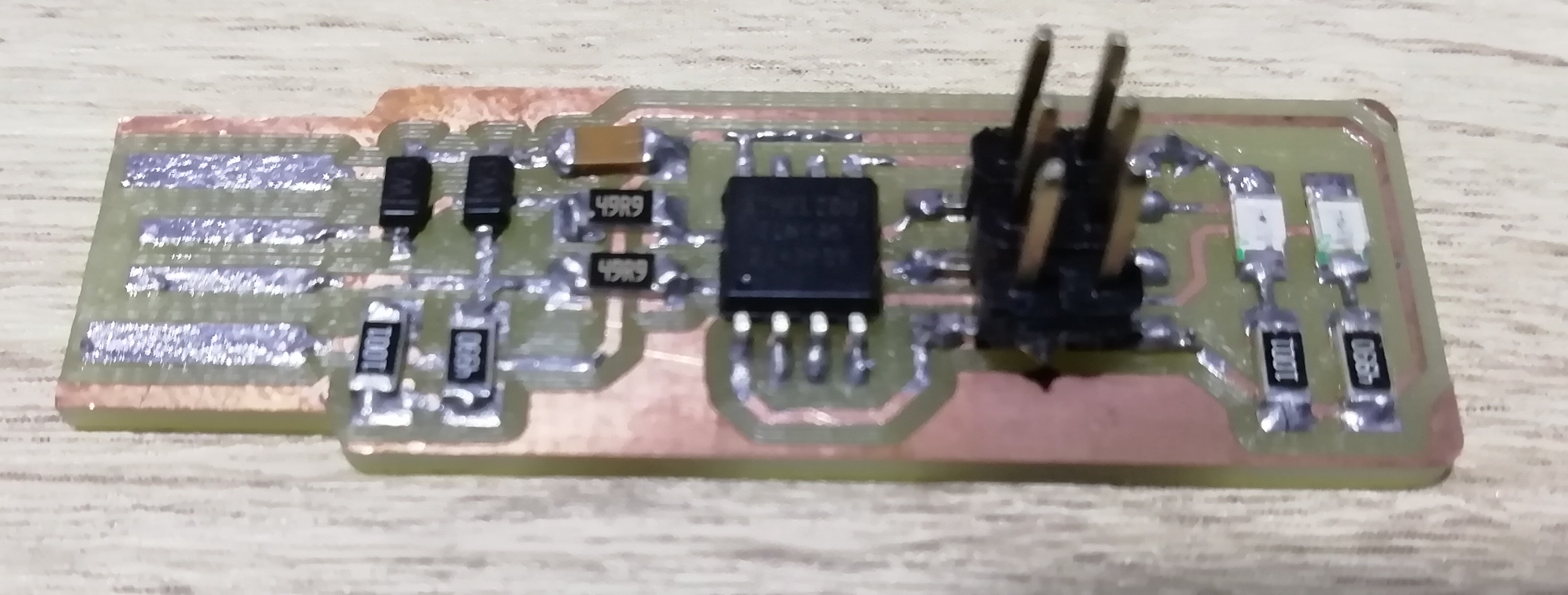
- Finally I have the PCB ready for component soldering.
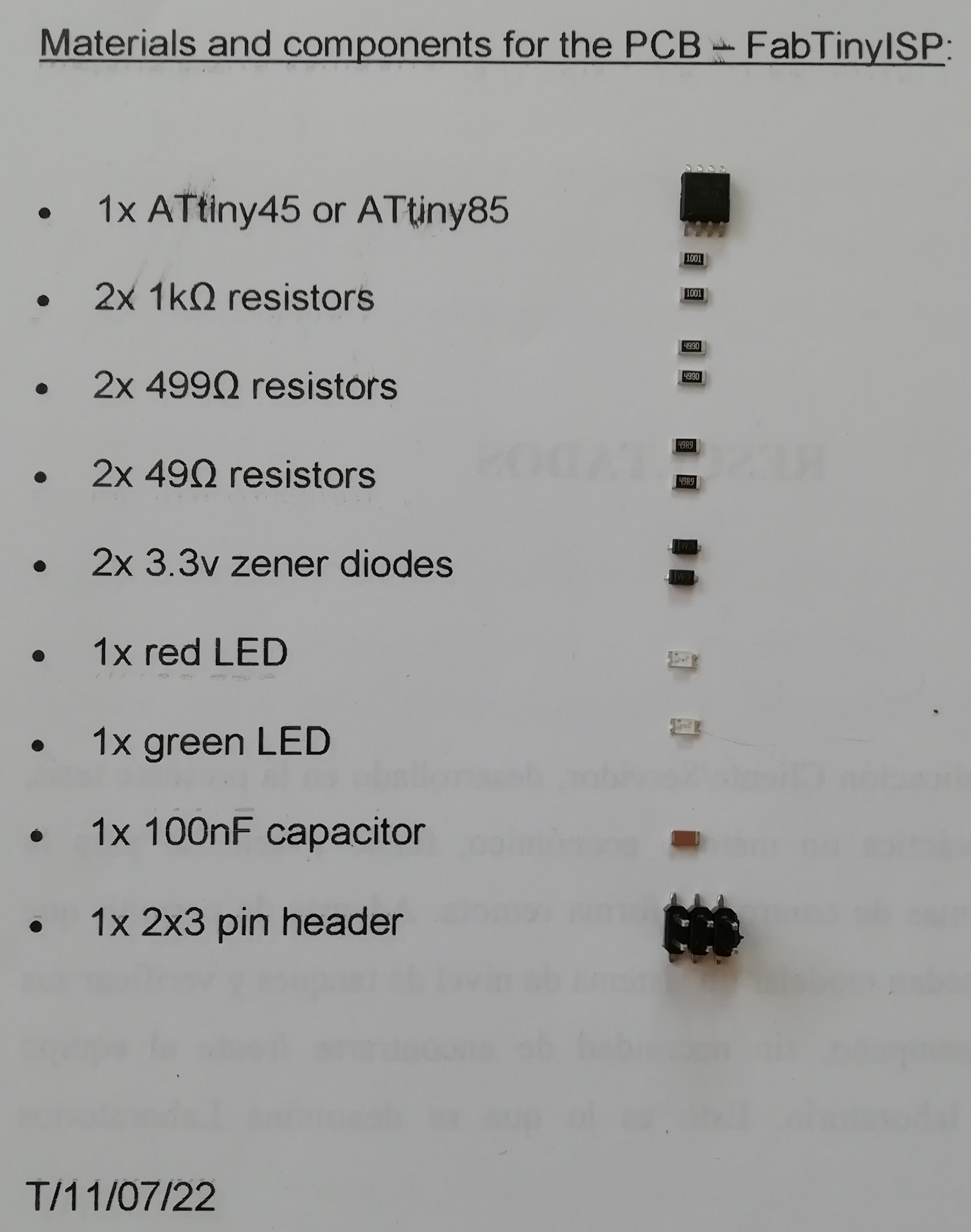
Components:
Work table

Soldering:
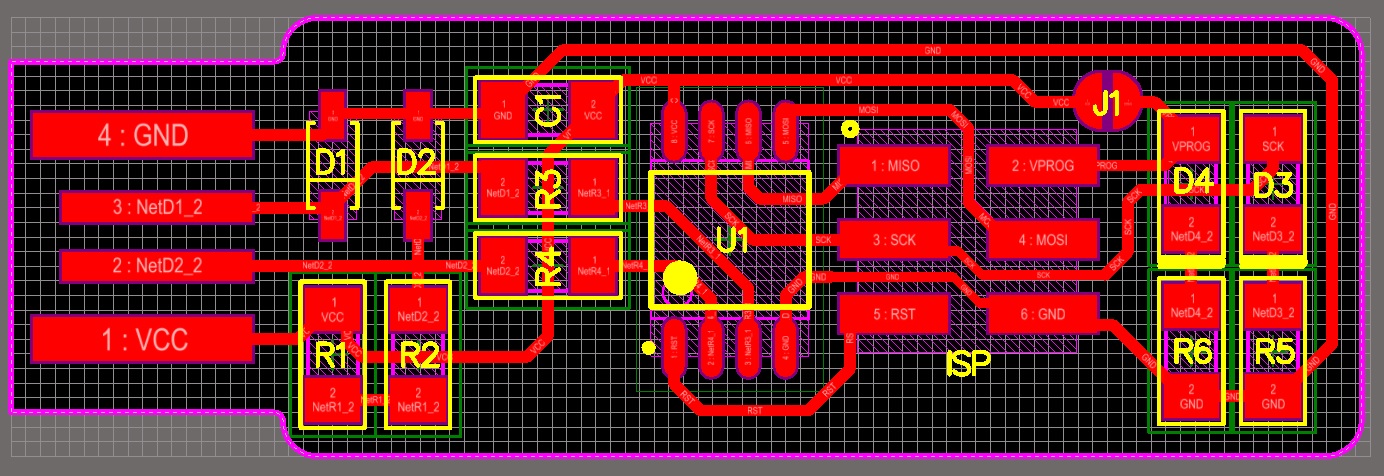
- I used this board layout diagram as a guide to determine where all the components would go.
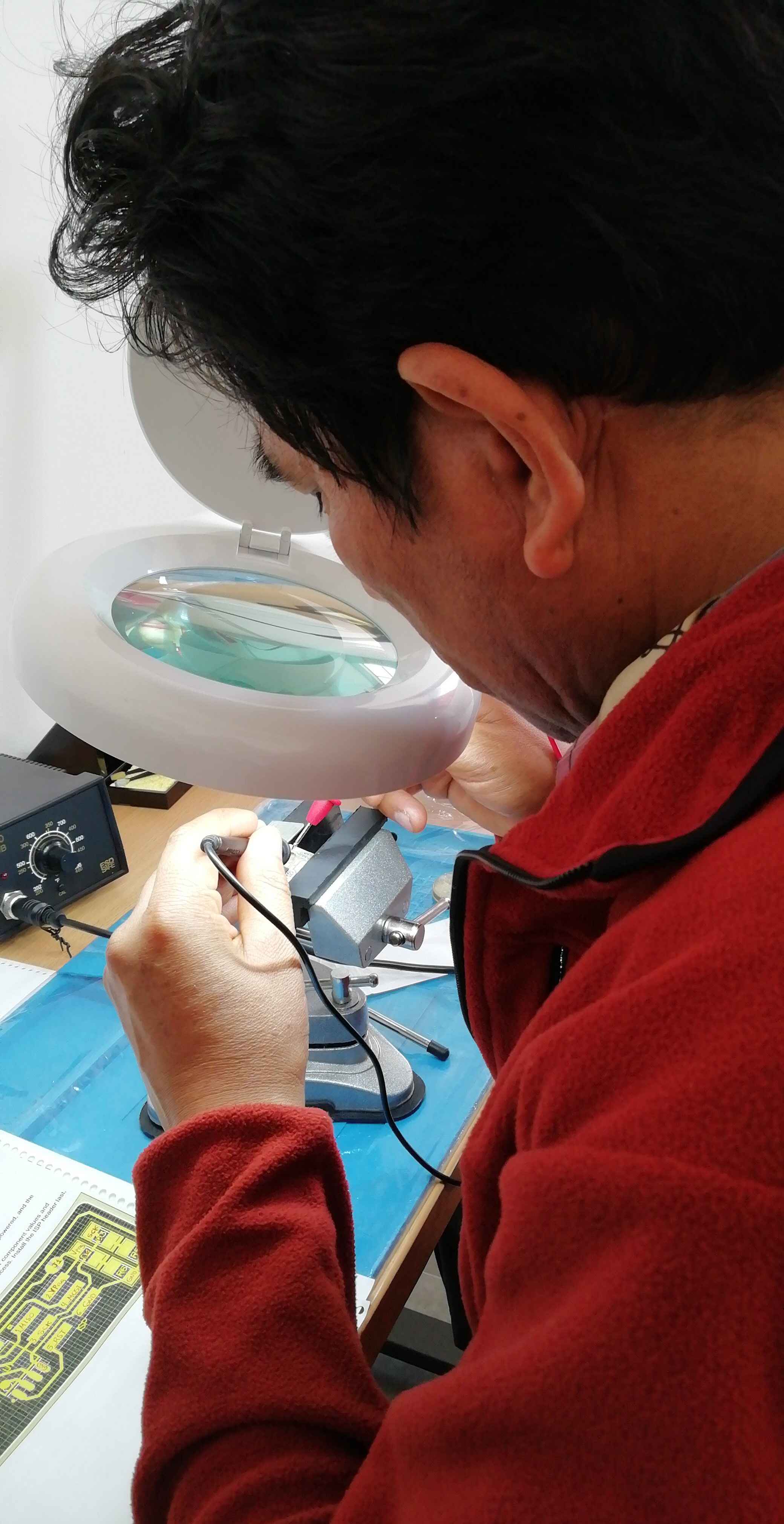
- I start welding, this takes time.

- I had previously soldered perforated PCBs, this is the first time I have soldered SMD components.
- I remain. Jumper J1 and the USB connector are missing.
- Final tinning. Cleaning with a small brush with isopropyl alcohol is recommended.
-
I test with the multitester if there is any cut between the tracks before testing if.
-
Here it is the final result , i think i did it well.
Programming Board:
For this, take as a reference the work of Amal Saidani. The first step is to download 4 programs:
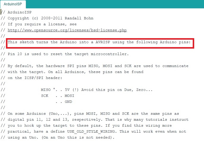
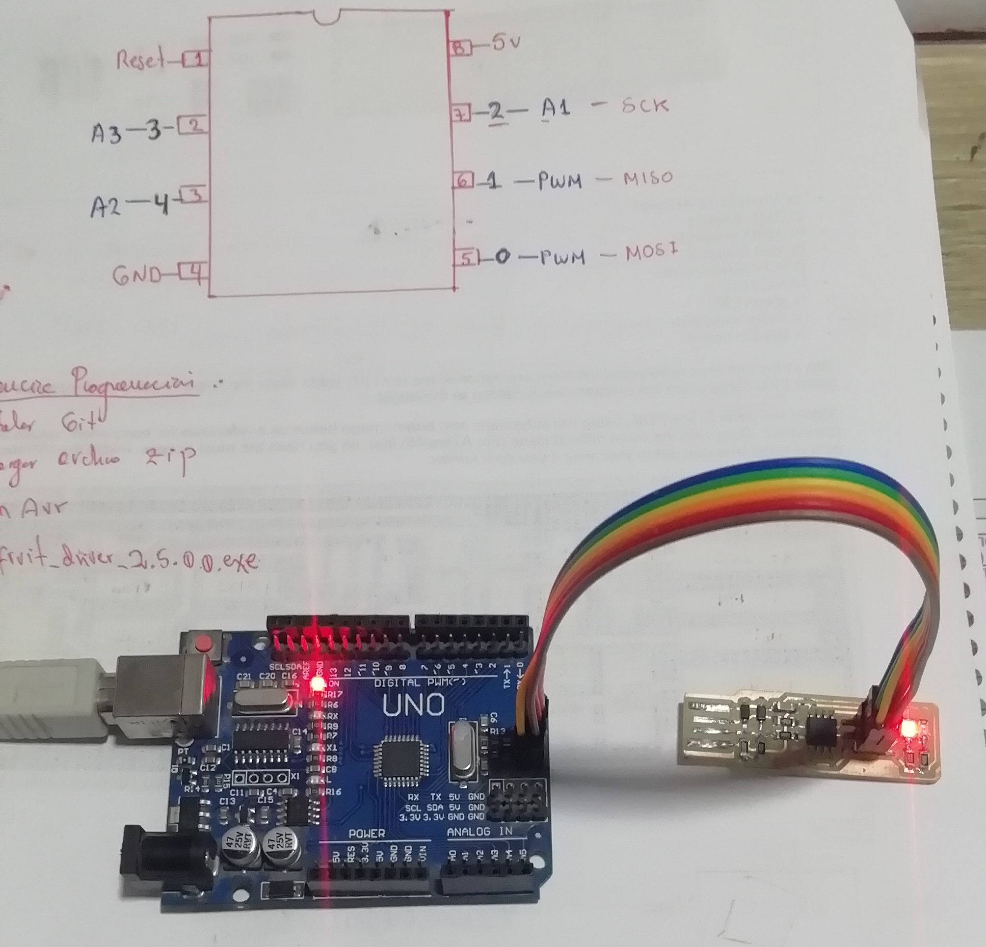
Arduino must work as ISP. Connect the arduino to the computer. Go to Arduino software: File -> Example -> Arduino ISP (This code makes the Arduino as a programmer)

- I upload the ISP file to the Arduino.
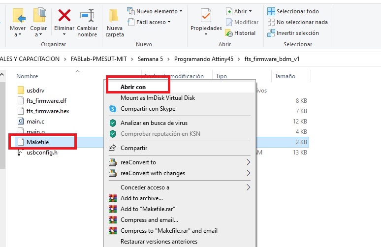
- Disconnect the arduino and go to the notepad file, this file is made for the ISP that ‘s why we need to make some changes so it becomes able to work with arduino .Before that you need to extract the Zip files (fts_firmware_bdm_v1.zip) that you downloaded previously.
- We open the makefile with notepad and make some changes so that the Arduino works as an AVR Programmer.
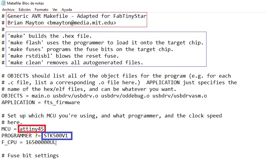
The programmer must be STK500V1
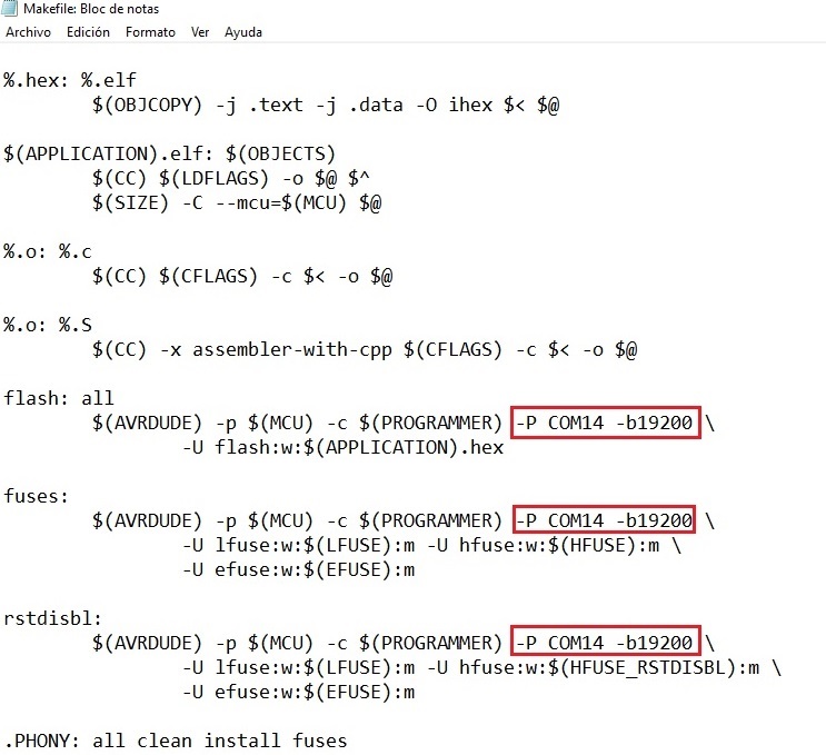
The speed bps 19200
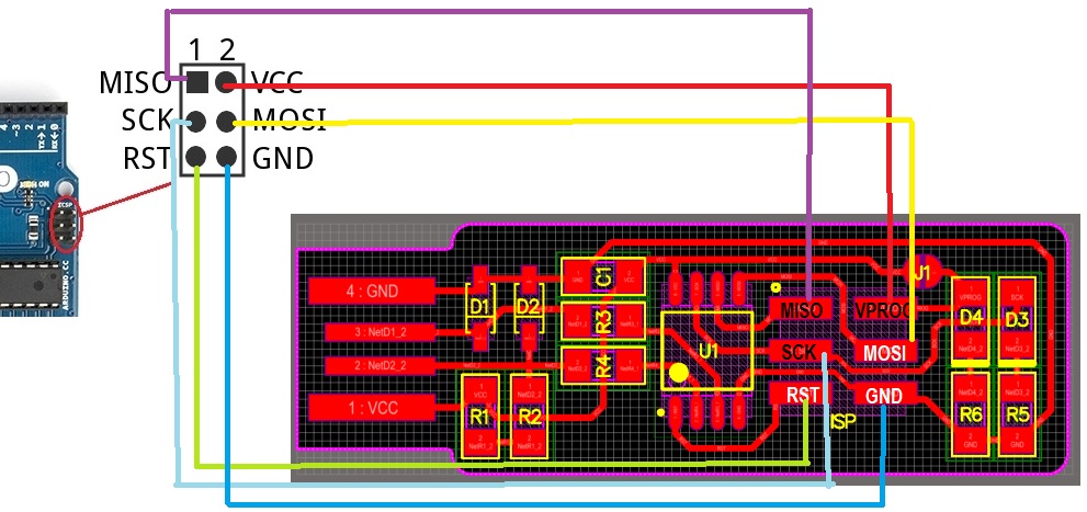
- Save the changes. Connect the Arduino with FabISP using jumper cables following the connections below and reconnect the Arduino to the laptop.
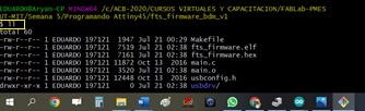
- Now, you need to reopen the same folder as before (fts_firmware_bdm_v1.zip) and right click and select Git Bash Here.

- You need o write the two commands LL to check your position and Make to check files.
- After checking that every thing went alright with the two commands you need to enter new ones but before that, you need to use a USB HUB,to connect your Arduino and your ISP together and then to your laptop.
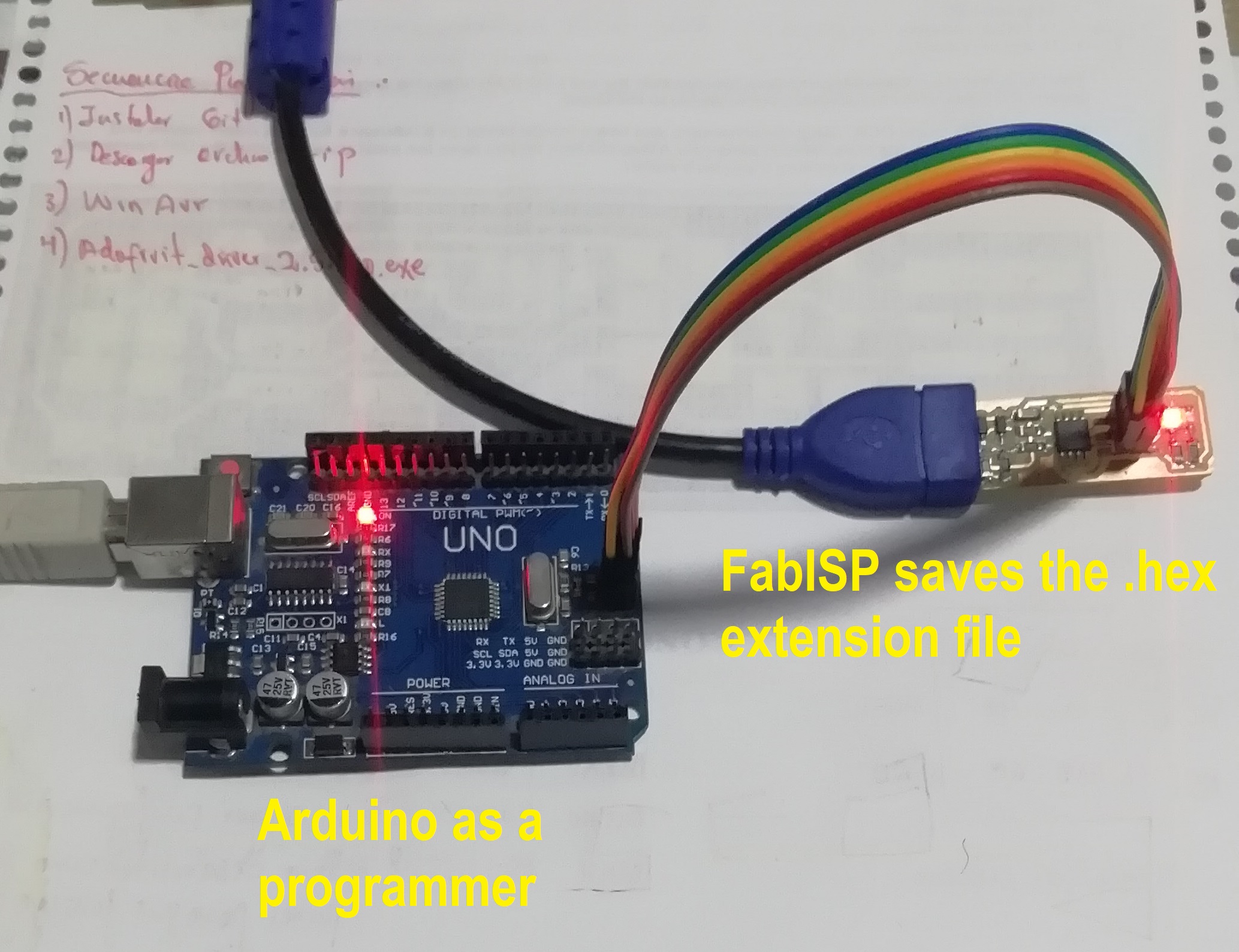
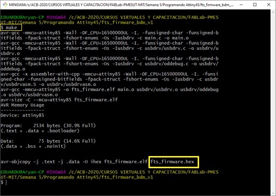
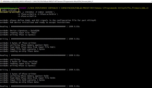
- Open Git and write special commands to program the ISP using Arduino:
# 'make' builds the .hex file.
# 'make flash' uses the programmer to load it onto the target chip.
# 'make fuses' programs the fuse bits on the target chip.
# 'make rstdisbl' blows the reset fuse.
# 'make clean' removes all autogenerated files.
make flash to send tje code to program the ISP
make fuses to upload settings
make rstdisbl to disable one of the pins to work as a reset
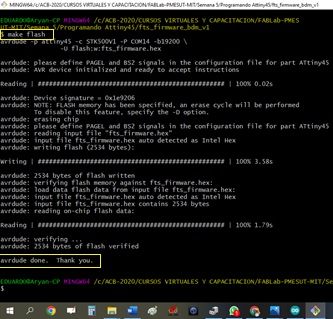
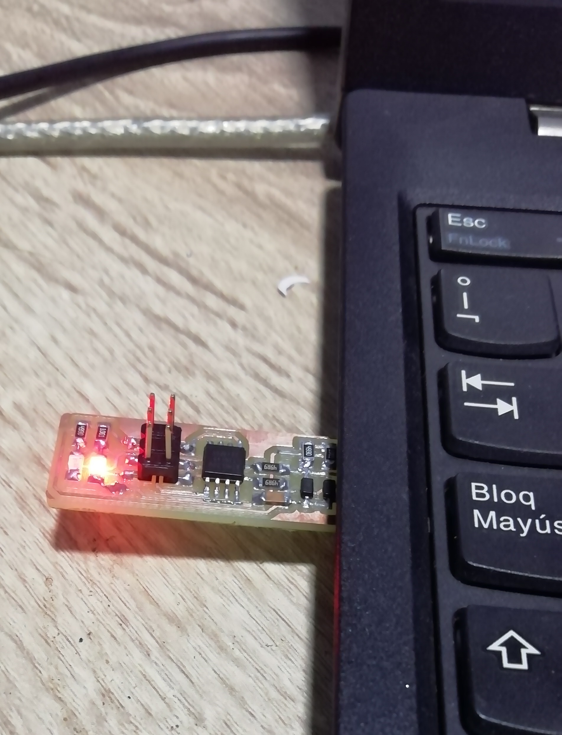
- You see your ISP LED (green and red) blinks so you can confirm partially the ISP programming , and yes the LED lights so i felt a little bit sure that i did the steps correctly.
-
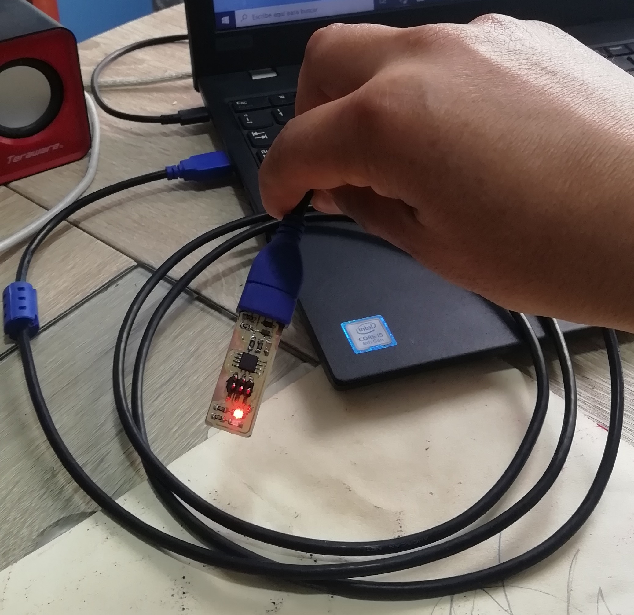
Now disconnect your Arduino from the Laptop’s USB port as well as all jumper cables and keep only the FabISP connected.
-
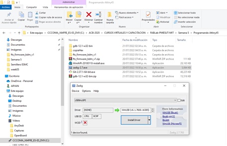
Use Zadig software to install the driver for the FabISP
1.- Find USPtinySPI
2.- Click Install Driver
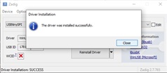
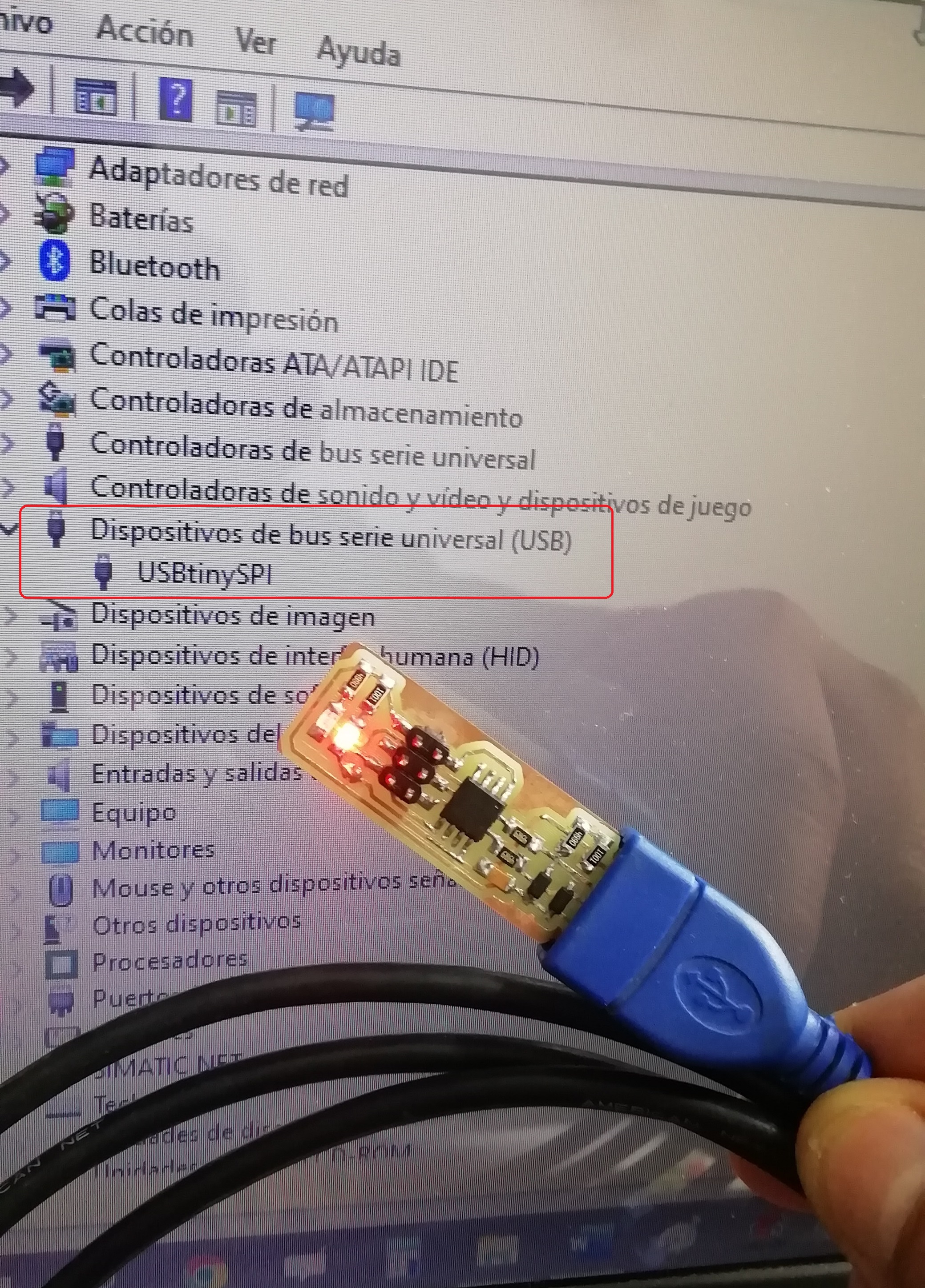
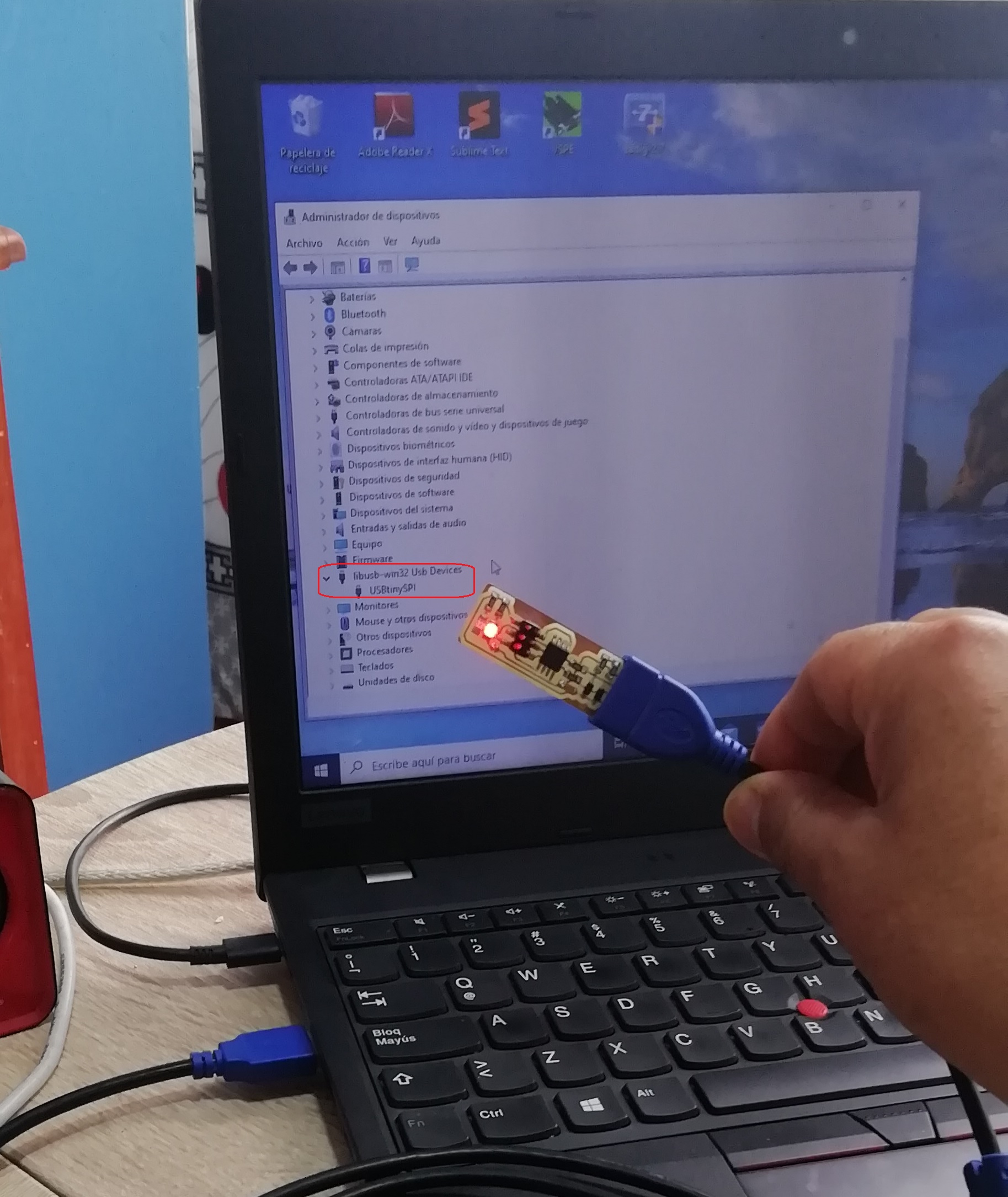
- Now the driver is installed so the FabISP is well programmed. To check if the ISP driver is installed you can go to: Device manager->libsub-win32devices and find USBTINYSPI
- So we finished our first programming board FabISP using the Arduino.
Programm blink new ISP with my programmed ISP:
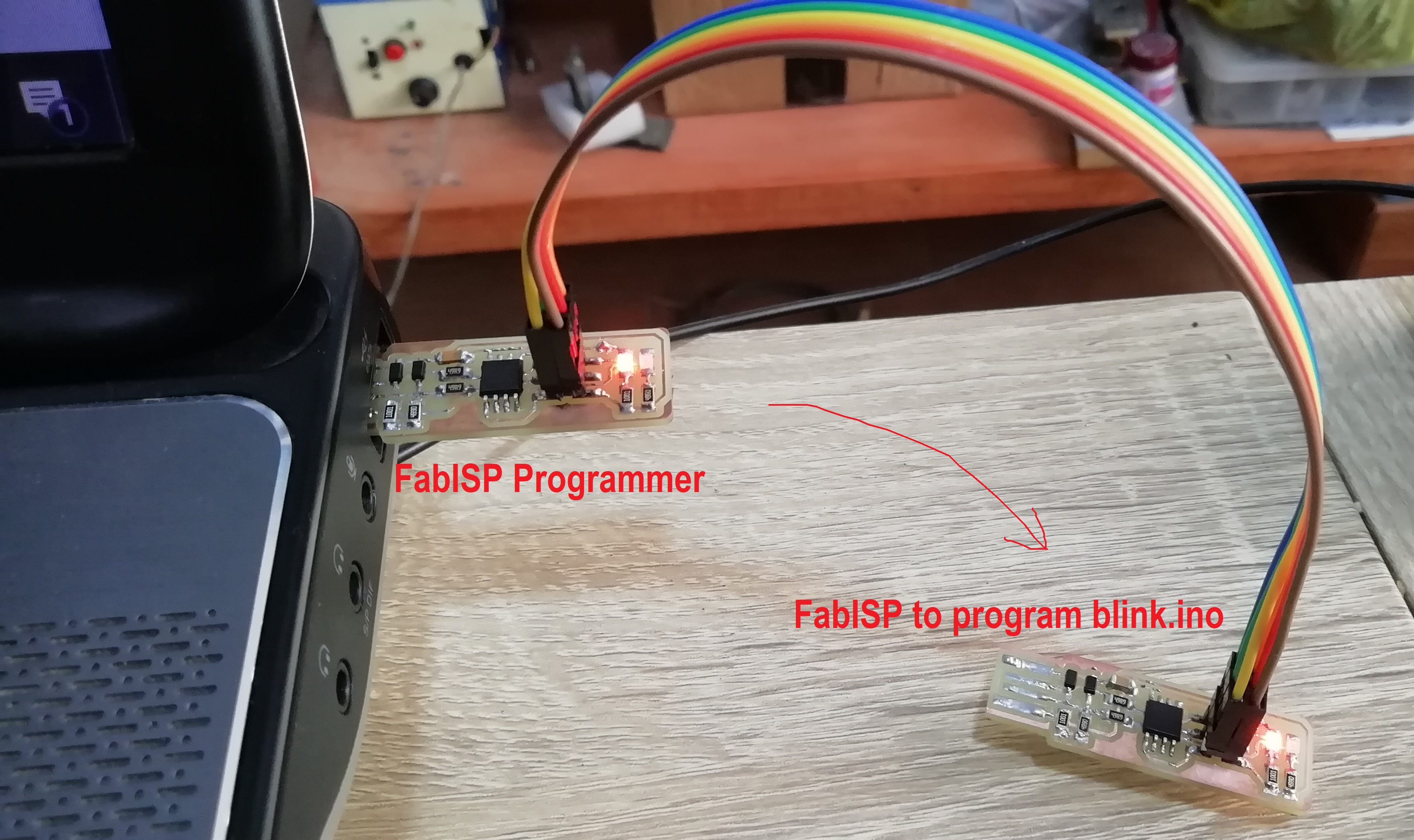
- I open the Arduino IDE, I see the example of blink LED. Address for pin PB2 of ATtiny 45.
//ATtiny45 PB2 (pin 7) blink

void setup() {
  pinMode(2, OUTPUT);
}

void loop() {
  digitalWrite(2, LOW);   // Turn the LED on
  delay(200);             // Wait for a second
  digitalWrite(2, HIGH);  // Turn the LED off by making the voltage HIGH
  delay(200);             // Wait for two seconds
}
- I transfer to the ISP to program
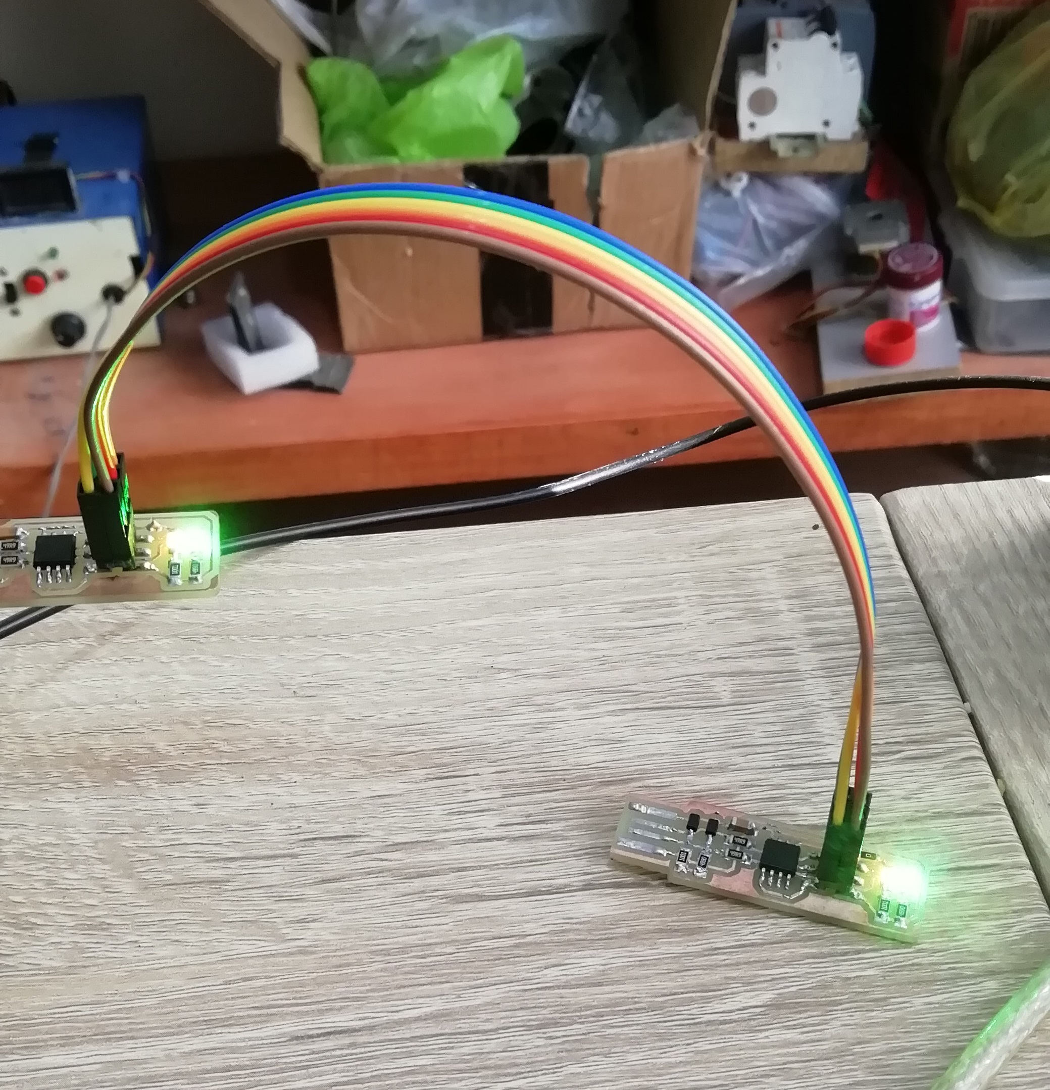
- A video demonstration of a classmate’s FabISP programming can be seen here. I make use of my programmer to program your card. wow!
-
So that the ISP can no longer be programmed and will always act as an ISP, either the J1 solder jumper or the 0 ohm resistor on the board must be removed.
-
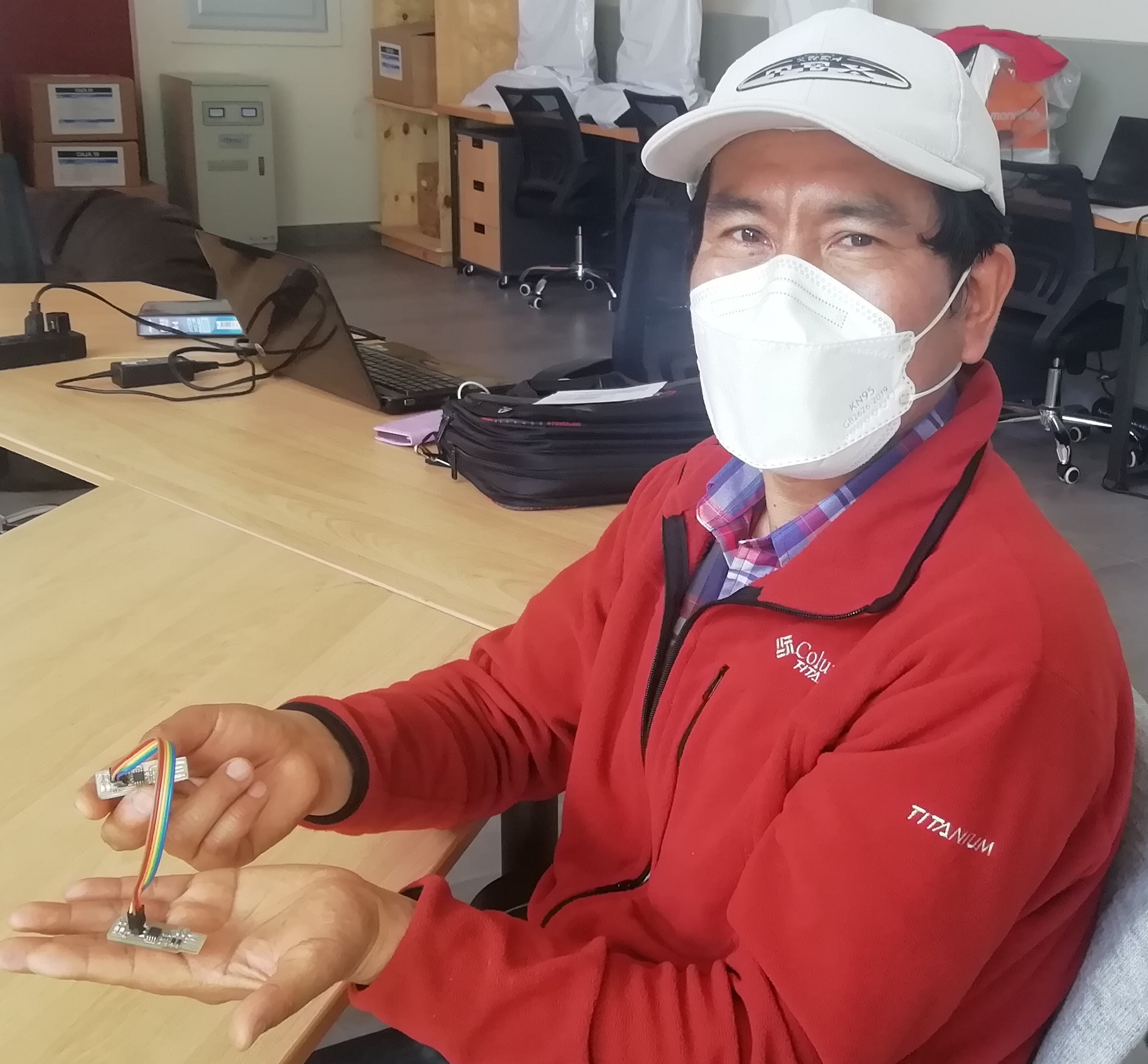
I finally have the FabISP in hand.
Additional:
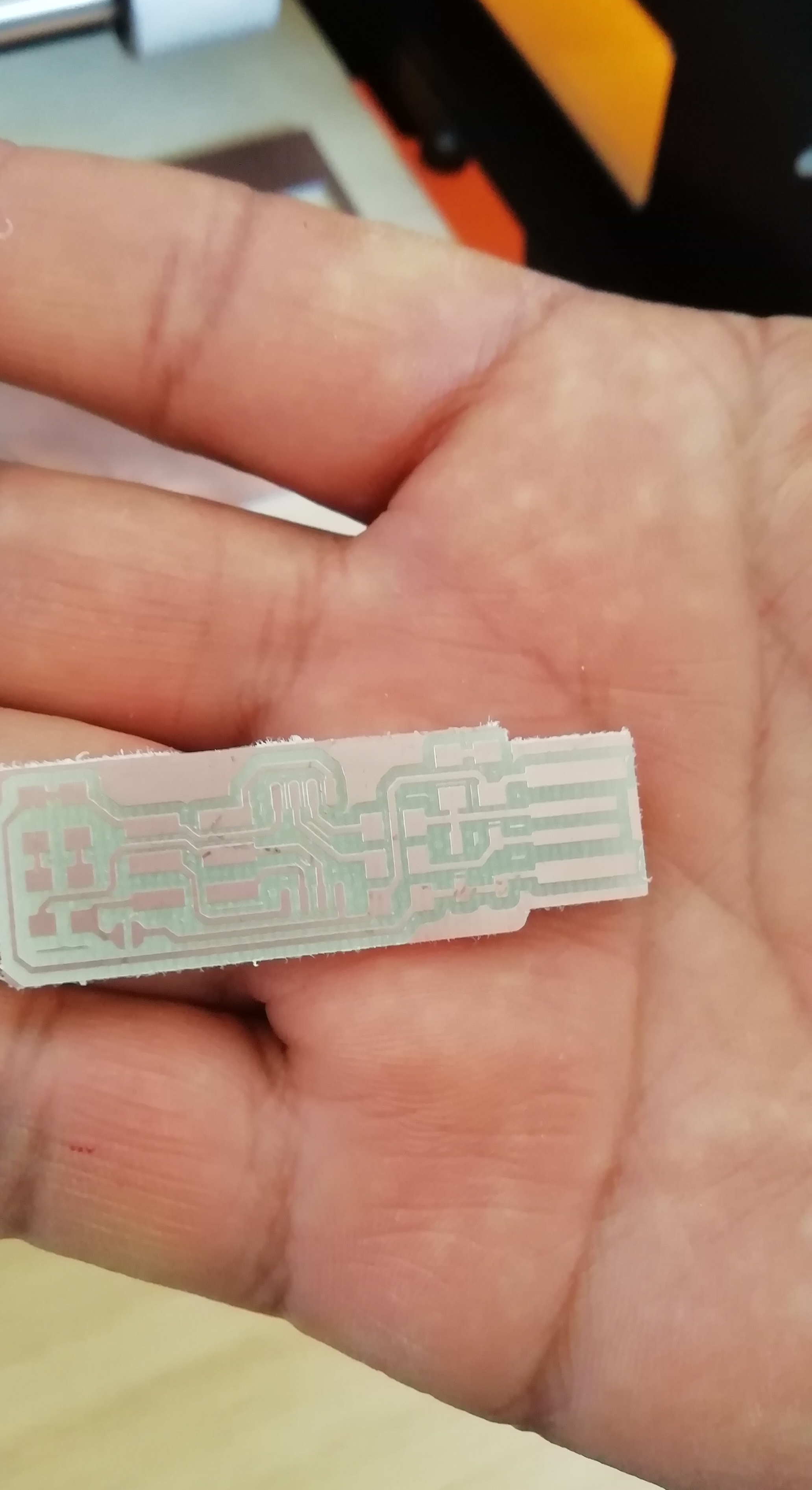
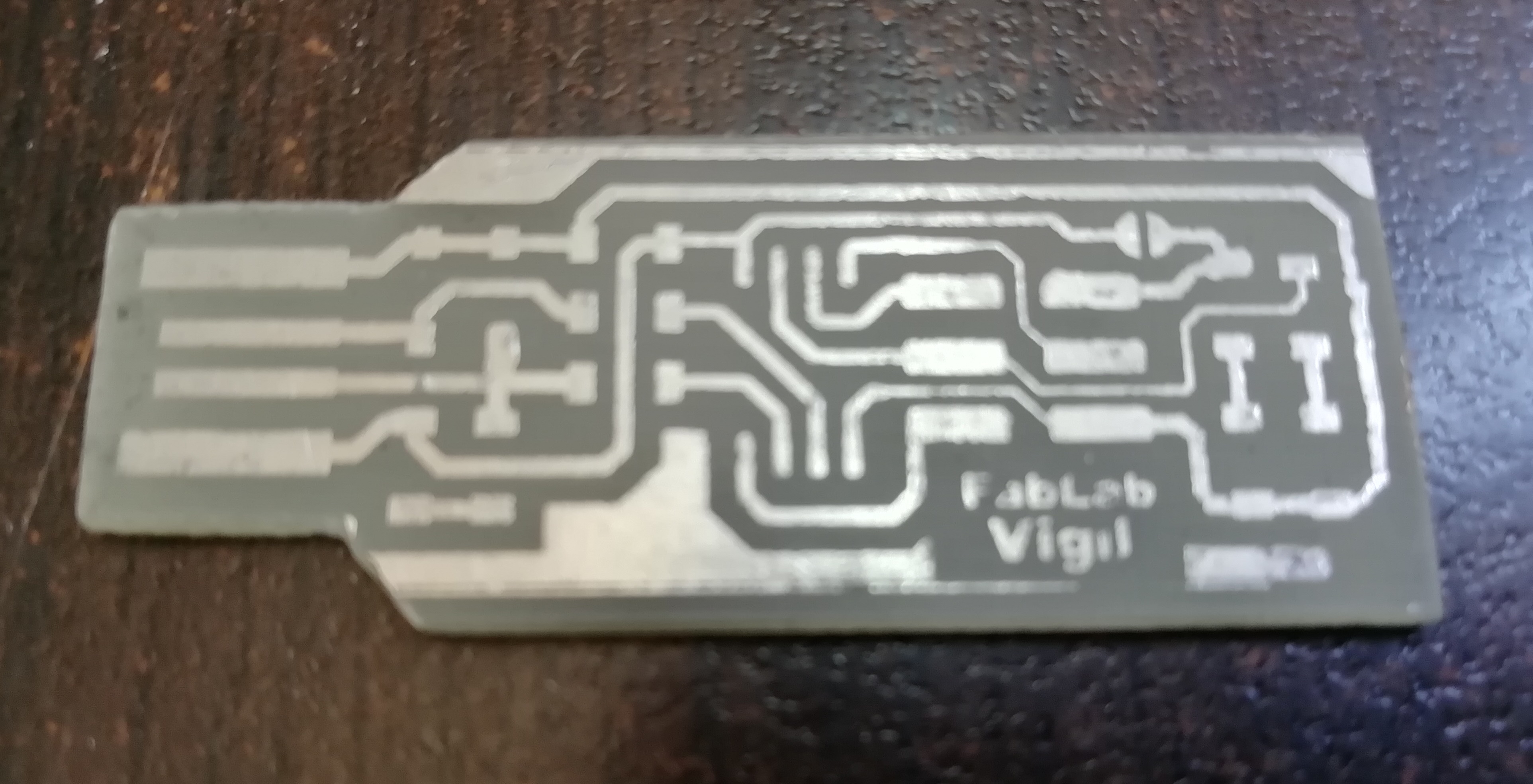
- Before the equipment arrived at the Laboratory, a PCB was made using the plate serigraphy process. This is how it looks:
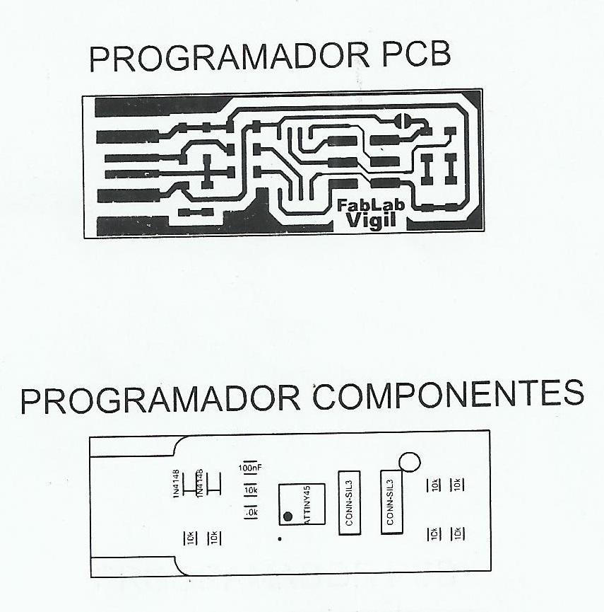
- This is a top view of the PCB by the silkscreen method.
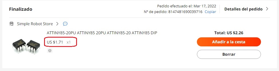
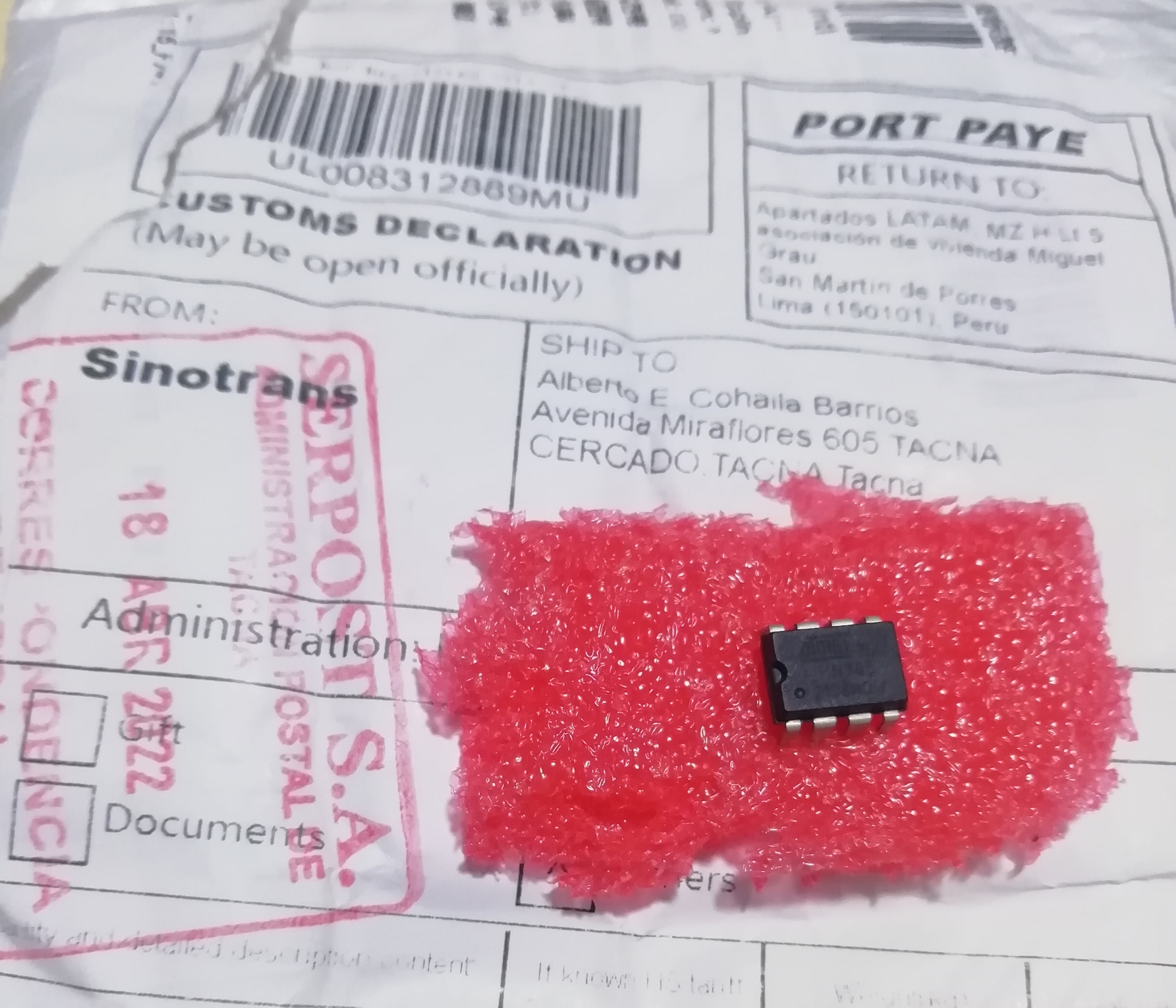
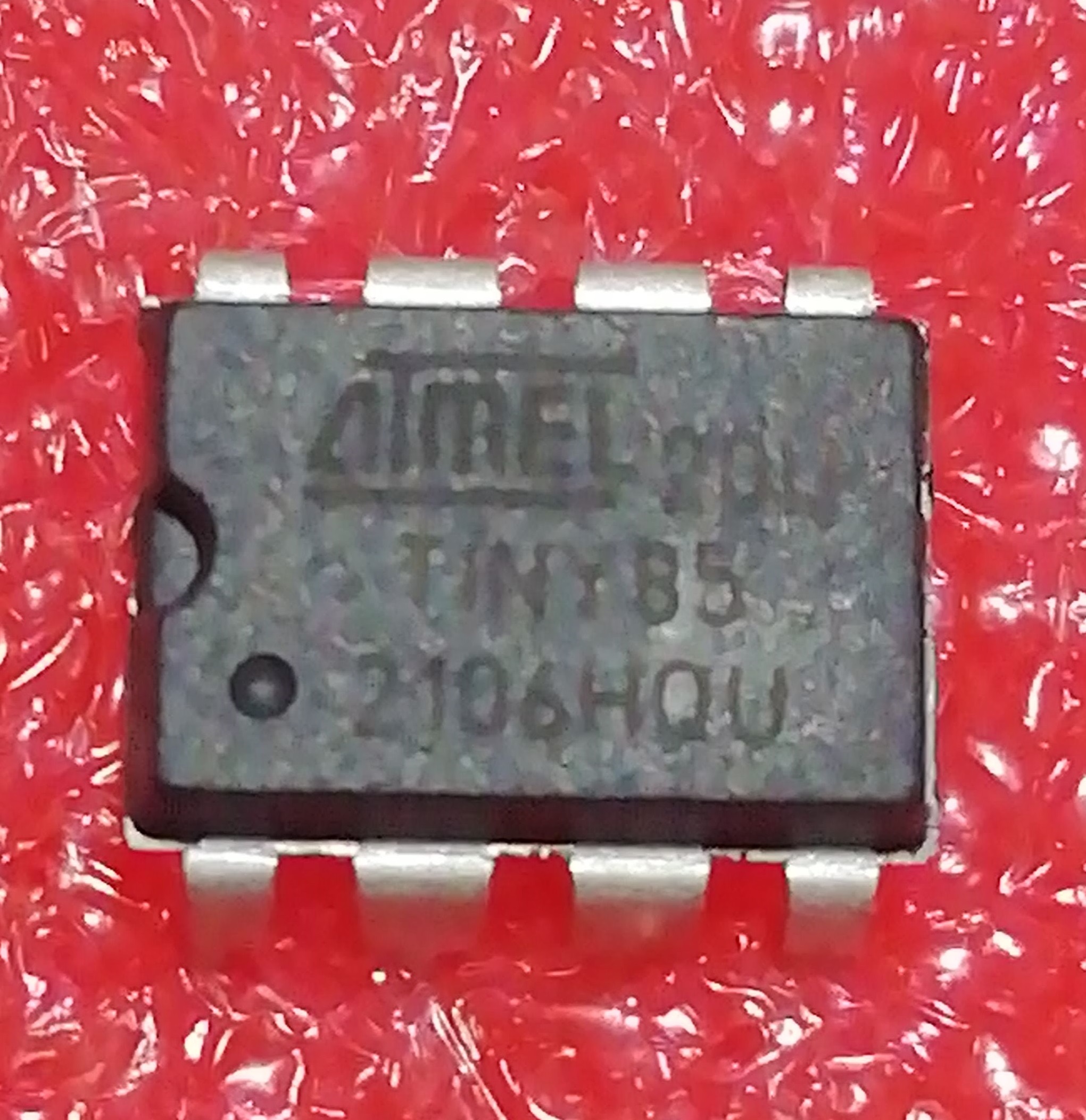
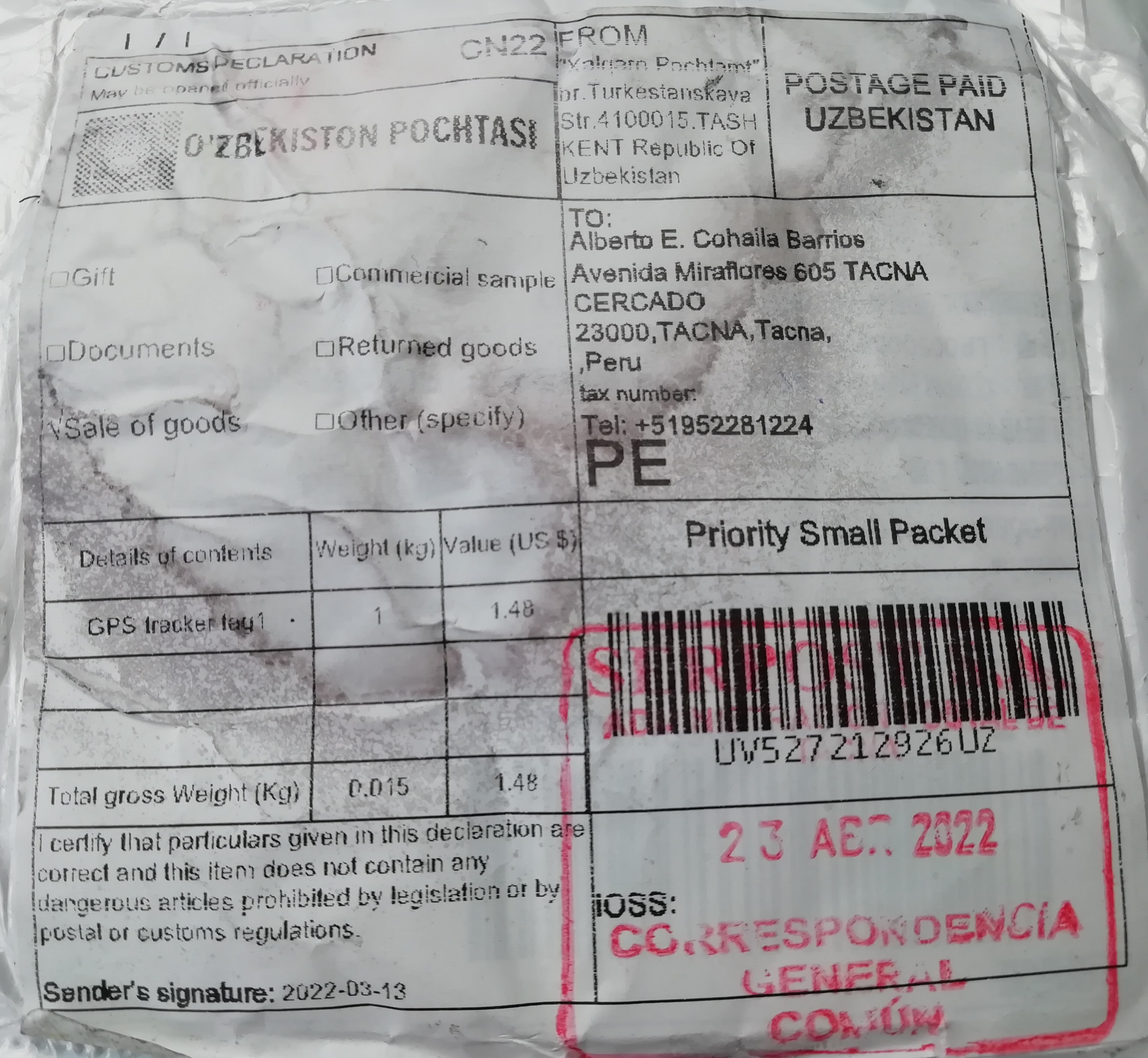
- We also ordered 1 ATtiny85 (DIP mount) through Aliexpress, which arrived after 31 days, on April 18, 2022.
- We also ordered 2 ATtiny45 (SOP mount) through Aliexpress, which arrived after 47 days, on April 23, 2022.
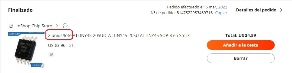
- Both arrived on April 18 and 23 respectively.
Design Files
| Description | Files | |
|---|---|---|
| Pattern_Test.png | Pattern_Test_PCB.png | |
| linetest.png | linetest.png | |
| linetest.png.rml | linetest.png.rml | |
| linetest.interior.png | linetest.interior.png | |
| linetest.interior.png.rml | linetest.interior.png.rml | |
| Git | Git | |
| WinAvr | WinAvr | |
| Zadig-USB | zadig-2.7.exe | |
| Zip file | fts_firmware_bdm_v1.zip |