5. Electronics production
Assignment
group assignment: characterize the design rules for your in-house PCB production process extra credit: send a PCB out to a board house
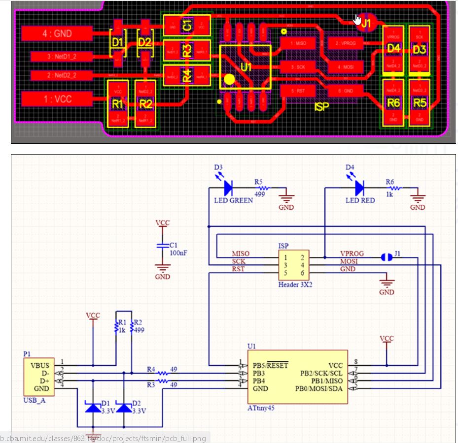
individual assignment: make an in-circuit programmer that includes a microcontroller: extra credit: customize the design mill and stuff the PCB test it to verify that it works extra credit: try other PCB processes
Download files :
FabISP firmware (from the Fabacademy site)
Gantt plan of the week
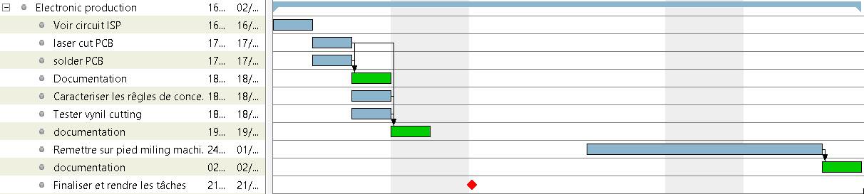
update
Adding the milling process which wasn’t initially planned
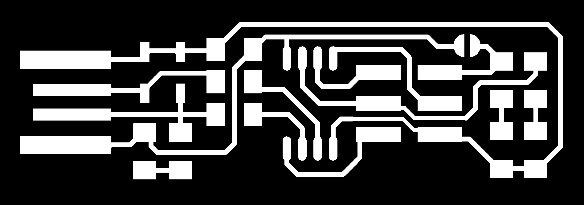
Building the FabTinyISP
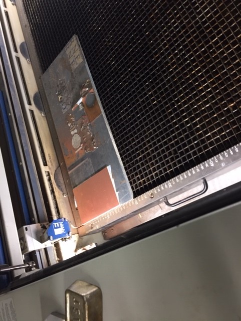
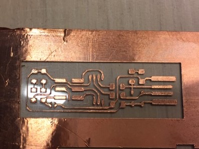
Laser cutting the PCB
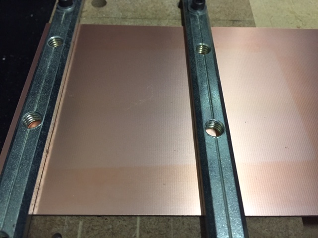
We use FR4 material and the fiber laser cutter to cut the traces.
I’m going to build the FabTinyISP from this tutorial
I documented last week how to use the laser cutting machine.
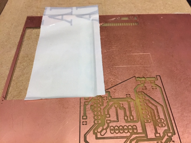
To fix the PCB on the board, we use double sided tape. When applying the tape, we need to make sure that there aren’t any bubble under the PCB because the laser cutter has a very precise focal point :
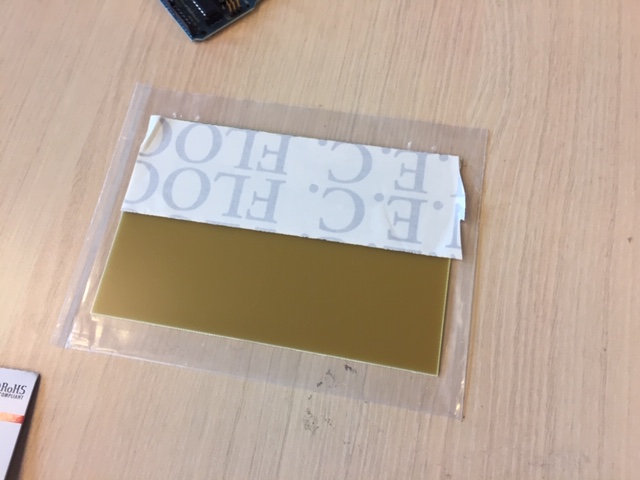
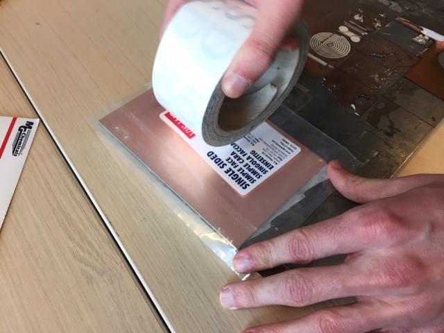
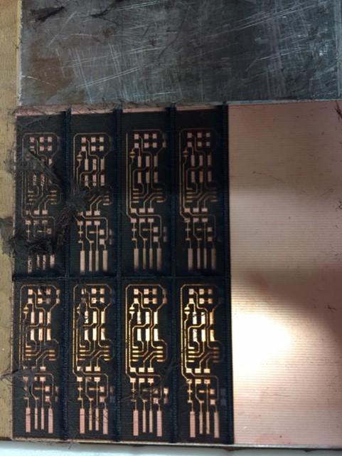
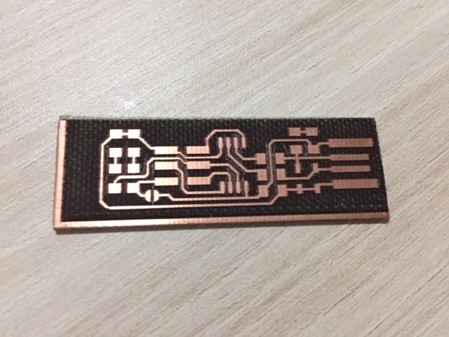
Then, we laser cutted the PCB after importing the png file of the traces :

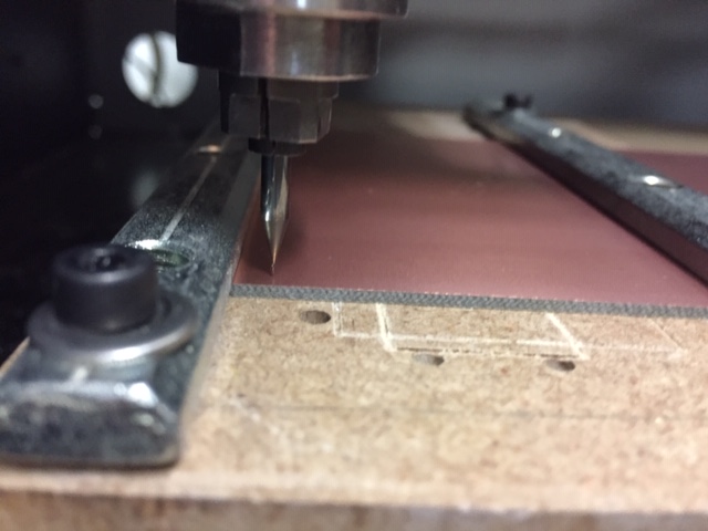
Calibrating the height
To calibrate the laser focus visually, we have to move the tray until we see a green bright light as you can see in the next video :
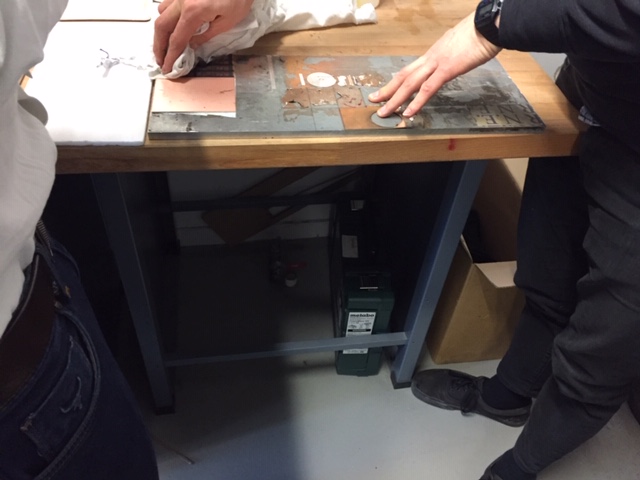
There are a few steps of post process :
| Wiping the card with Alcool | Removing the PCB |
|---|---|
 |
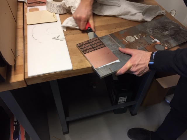 |
When the PCB is in the machine, it’s difficult to see if the laser cutter went through the PCB. When we remove the PCB from the laser cutter it wasn’t cut through. So we finished with the knife cutter.
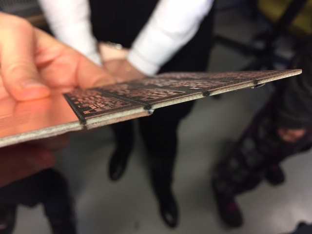
We also had to use the knife cutter to remove any residual copper that subsisted between the wire trace. And test the absence of continuity between the trace.
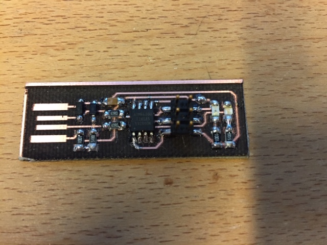
Soldering the components
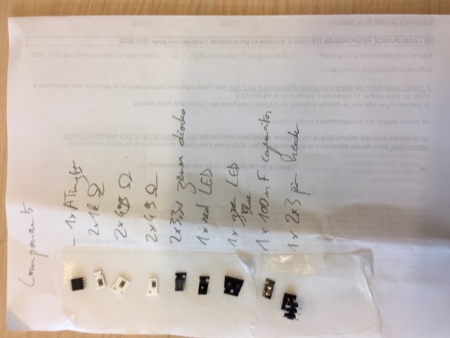
First, we started by making a list of components :
Then, solder according to the schematics :
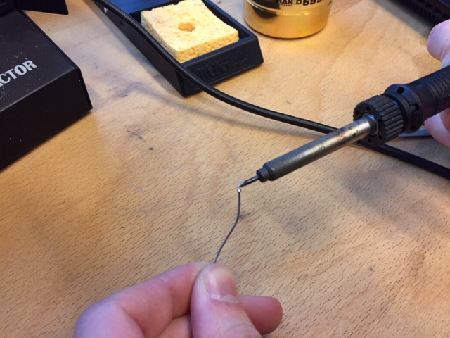
The material used to solder is an alloy of tin and lead. I started by the easiest components first, and soldered from left to right :
Then, our instructor gave us a good practice lesson of how to solder well. The iron should be in contact with the component as well as the copper. The soldering should look shiny :
Tin the tip of the soldering iron (Cover it with tin to enhance adhesion) :
Then add a bit of tin on the first pin (operation of tacking) and bring the microcontroller on it while heating the tin :
Make sure that the component is well placed for every pin. Then solder the opposite pin. Heat the pin and the emplacement on the board at the same time and a add a bit of tin on it :
| Solder the opposite pin | Atiny soldered |
|---|---|
 |
 |
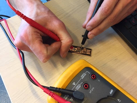
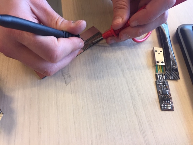
I tested the diodes with the continuity function of the multimeter to see what is the polarity :
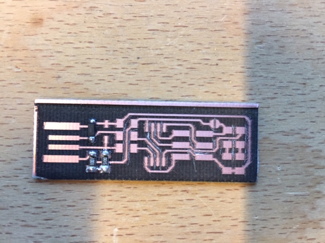
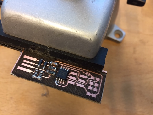
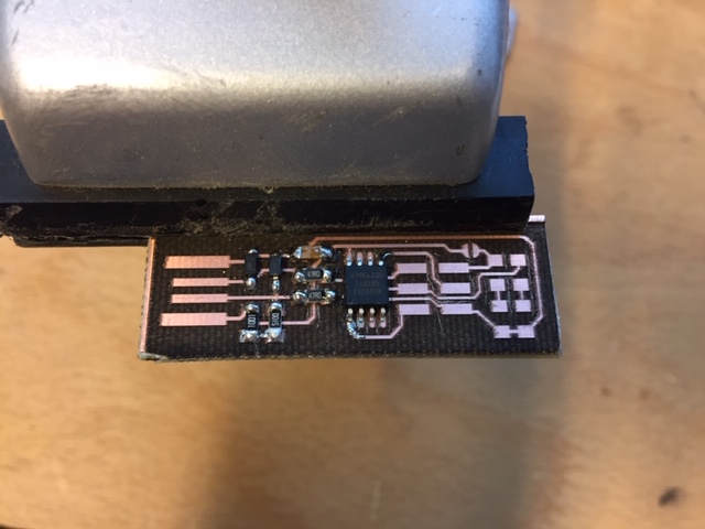
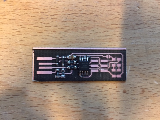
Finally, the PCB soldered :
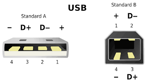
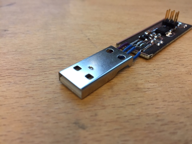
To solder the USB port, I checked a schematic of USB A for the orientation :
Programming the Programmer
To program the programmer, the first thing is to install Atmel GNU toolchain, GNU make and avrdude. For this week’s assignment, we used our instructor’s installation because he had everything working already. Here are the steps we’ve done :
Communicating with the USBtiny
First thing, we connect the USBtiny to the AtmelICE programmer with the 6 pin header and to the 5V current source with the USB connector :
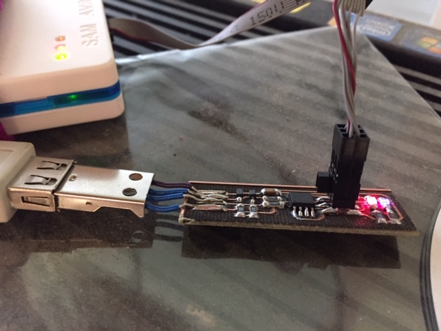
The led is light on, it’s a good start. In ATMEL studio, go to programming tool and select the device ATiny45 and AtmelICE for the tool. Click on read to communicate with the Atiny :
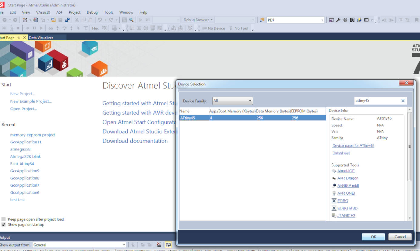
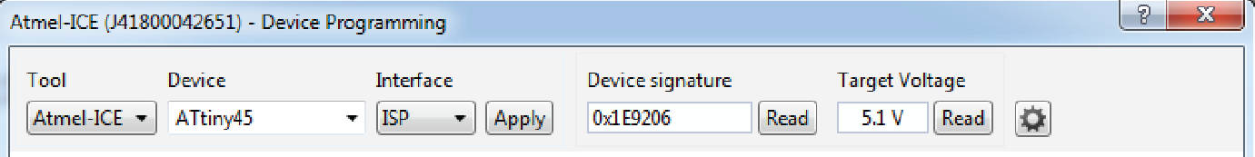
We have a device signature, it means that we can communicate with it !
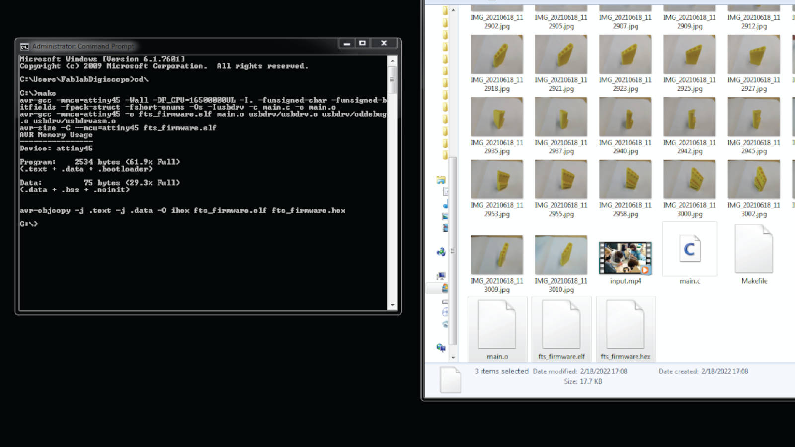
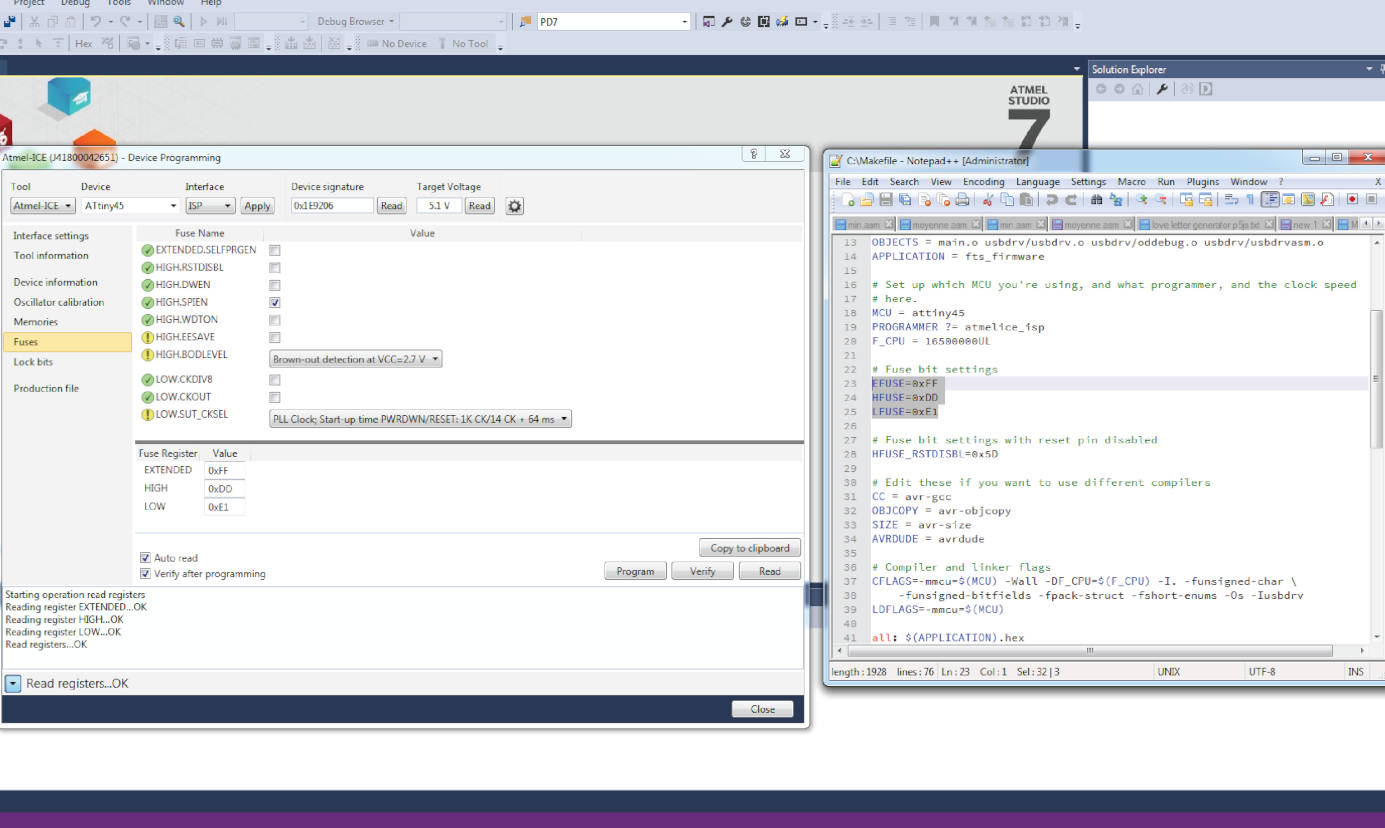
Adding the firmware + changing fuse
Next step, convert the firmware file in .hex with the command line make (be sure to be in the right folder) :
and add the firmware.hex in the memories tab :
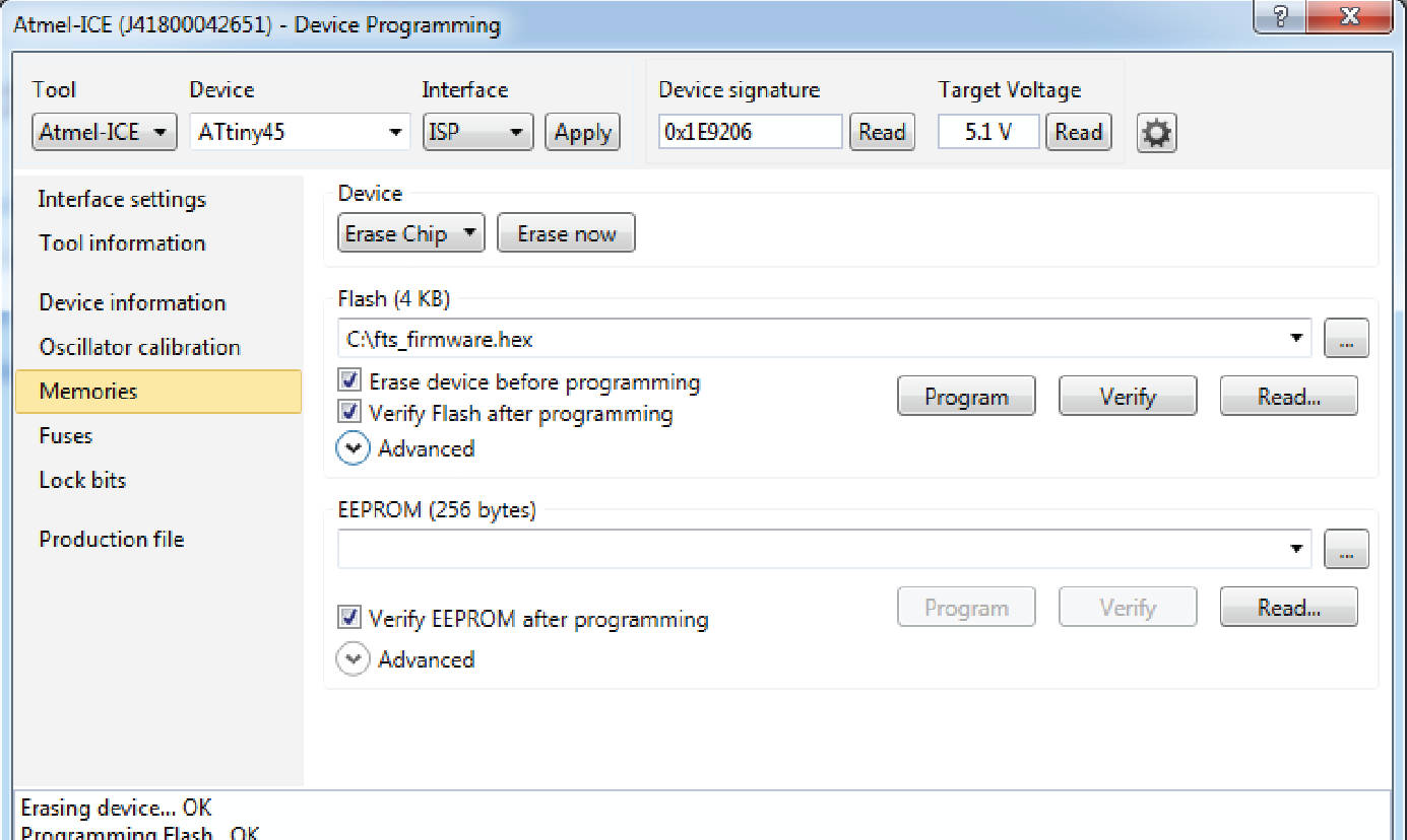
and select the good fuses :
After doing that, we should be able to read the device when connecting it to the USB port of the computer :
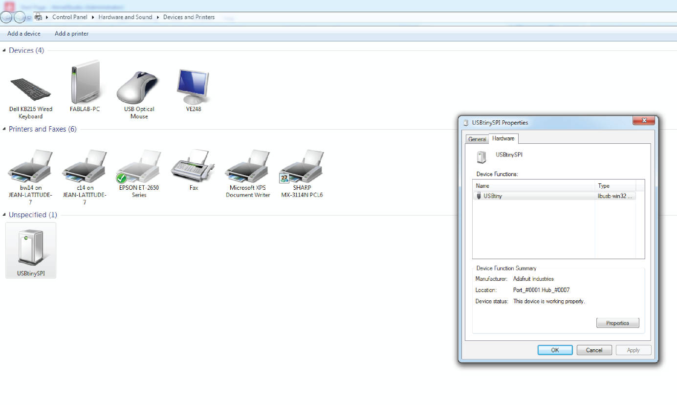
And we have it, USBTinySPI appears.
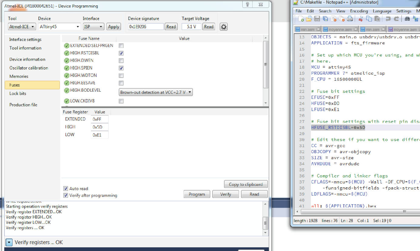
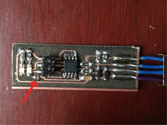
Changing the reset fuse and unsolder J1
The last step is to disable the reset fuse and unsolder J1 :
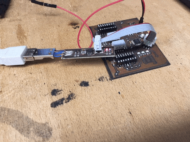
Testing the programmer
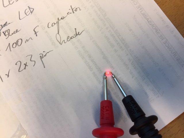
To test the programmer, we will program a microship atmega 328p with a blinking led program from the arduino IDE :
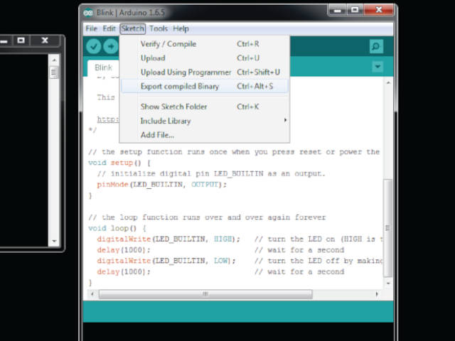
Then, we enter the command line
avrdude -c usbtiny -p m328p -P -com2 -U flash:v:blink.hex
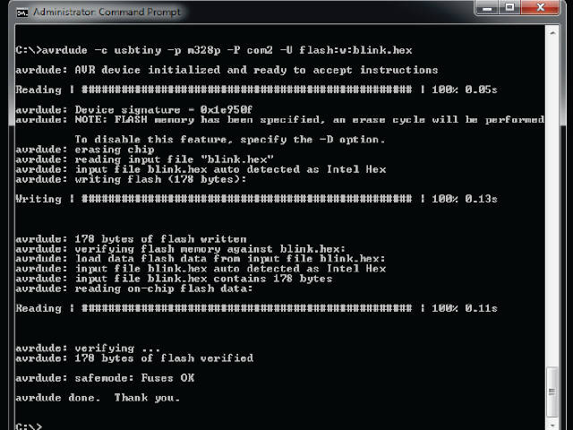
Finaly, the result in gif :
Group Assignment
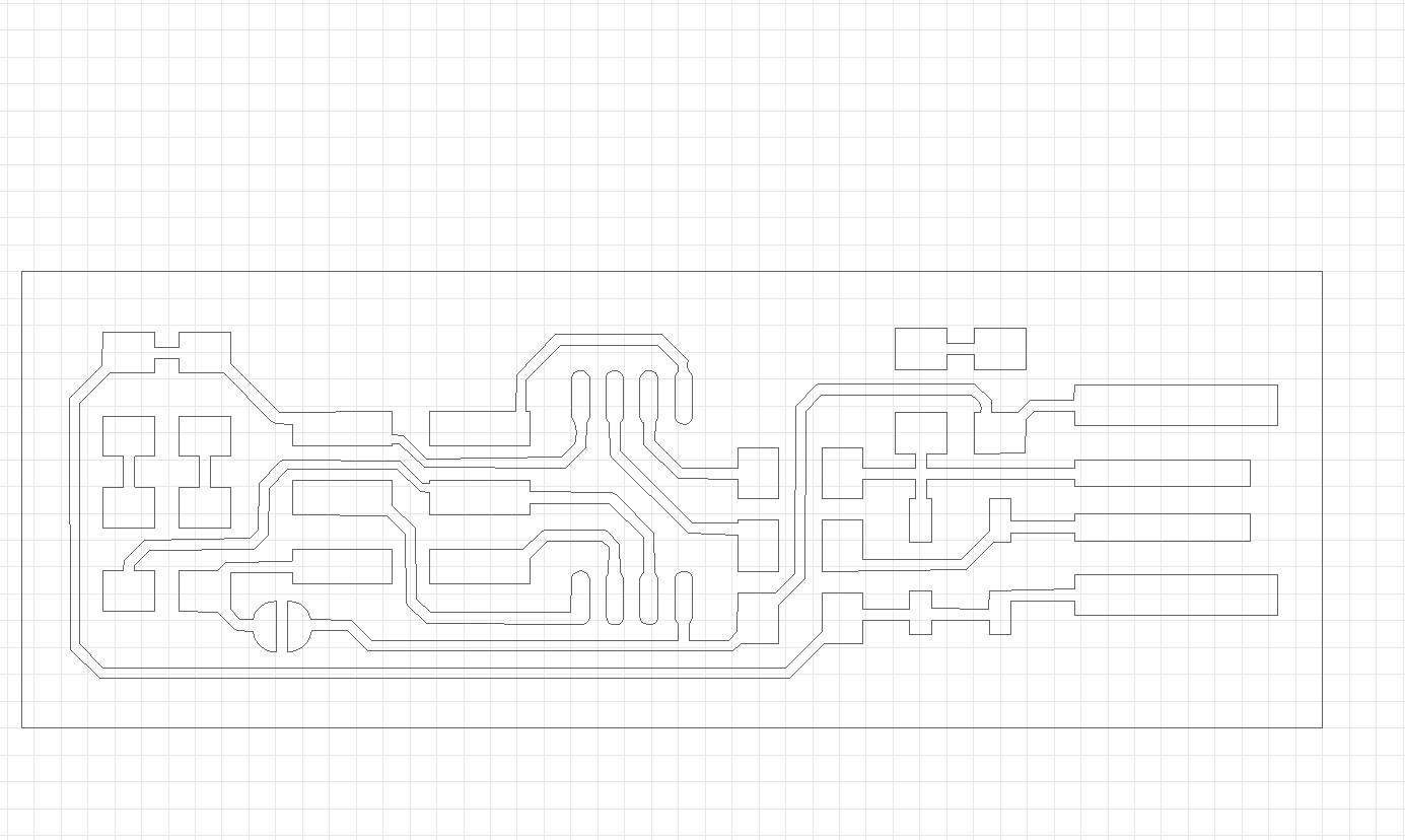
In the fablab Digiscope, the PCB production is made with the laser cutter thanks to the fiber cutting.
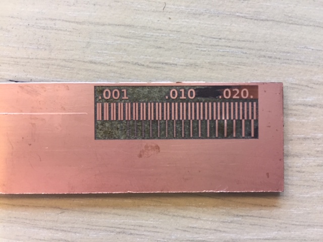
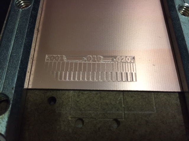
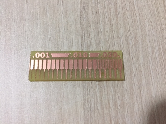
For the group assignment, we will use the linetest file to characterize the precision of the machine :
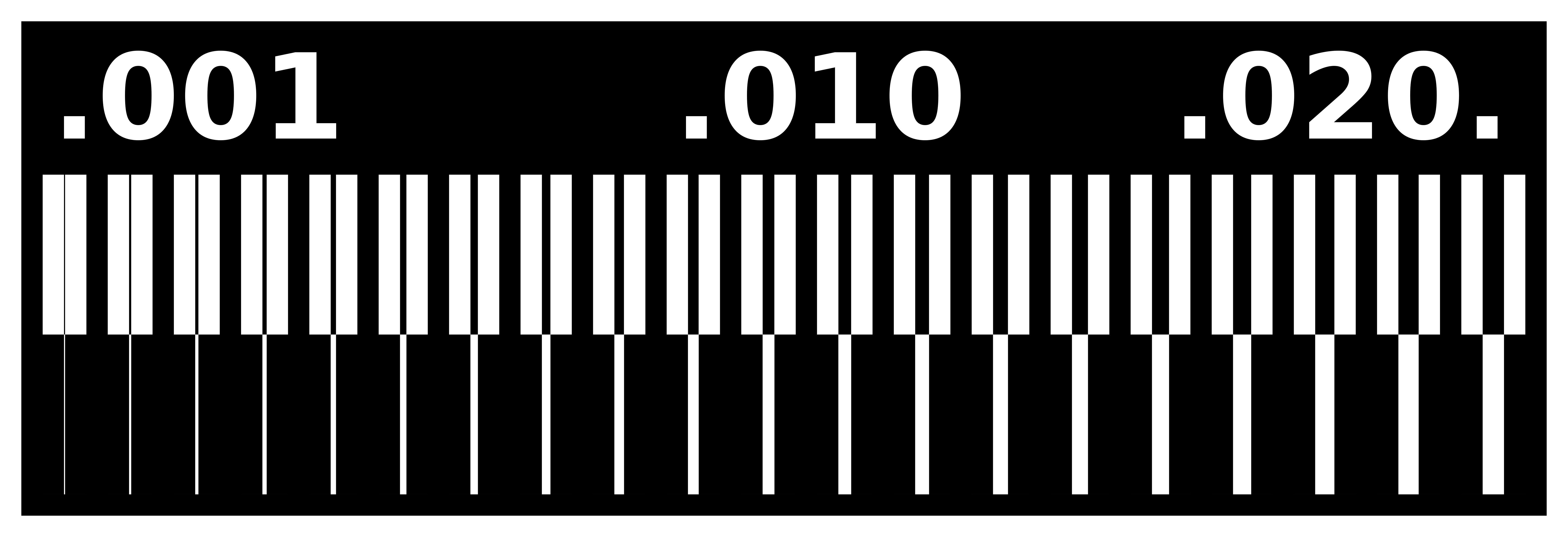
Then, we did a first test with the following settings : 10/100/1 (for speed/power/frequency) and 1200 dpi. It is made in 2 passes :
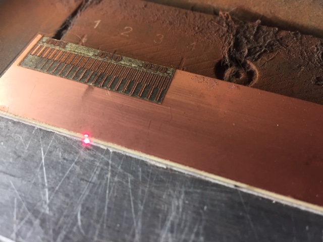
Here is the result :
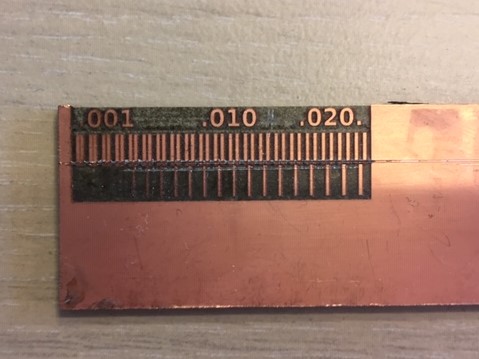
The finer part looks like this in the microscope :
We tested the connection between each lines and there were continuity until .014 inch :
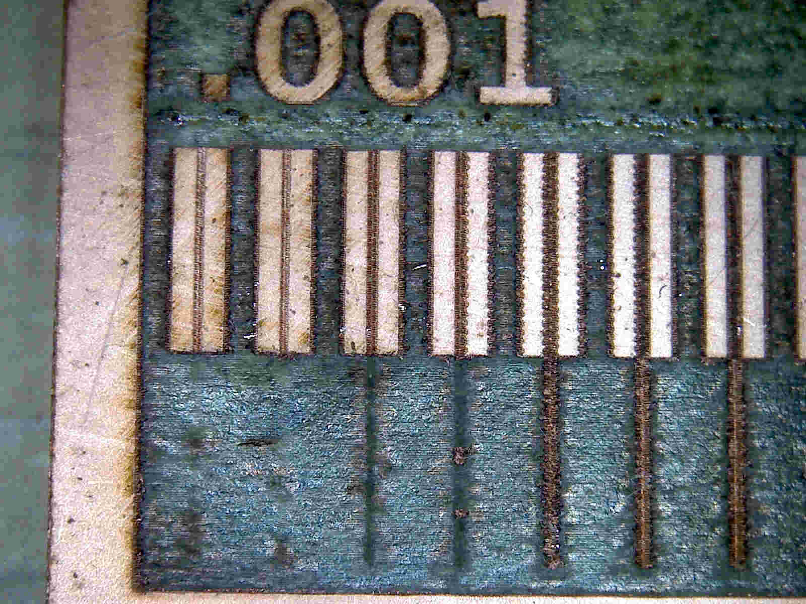
So we made another test with the same settings but 3 passes this time :
The finer part looks like this in the microscope :
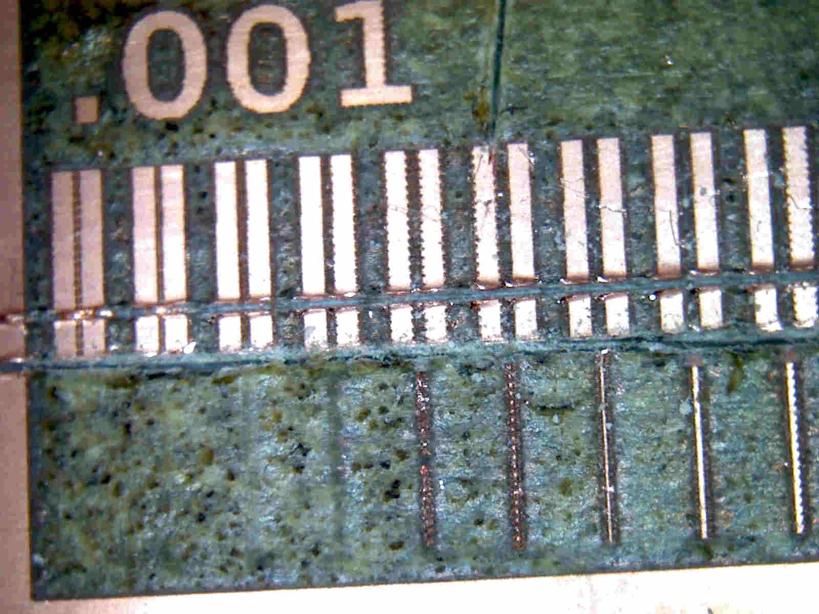
There was no continuity until the mark at 0.006 inch. The knife cutted trace you see was made to be sure that there is no contact between the bottom line and the two upper lines.
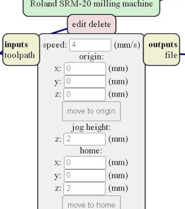
Other PCB process : Milling machine
Even though the PCB cutting process is made with a laser cutter in fablab Digiscope, there still is an (old) Roland Mdx-40 in the fablab. Thanks to the help from Romain, director of the fablab and Fabacademy Guru, I reenacted the machine :
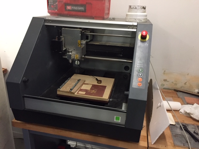
The machine is controlled by the Vpanel software :
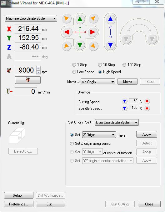
Setup the bit and origin
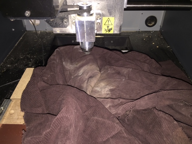
First thing, put the milling cutter into the tool holder. I used a piece of cloth for safety to not brake the bit if I drop it :
Then, defining the XY origin and Z origin. To do the Z-origin, I made a “bit drop” : lower down the mill cutter close to the PCB and loosen the bit to make it drop to the PCB and then tighten the bit again.
| XY origin | Put the bit close to the PCB | Drop the bit to touch the PCB |
|---|---|---|
 |
 |
 |
Click on apply origin in Vpanel
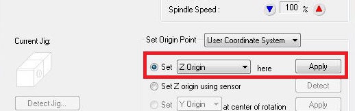
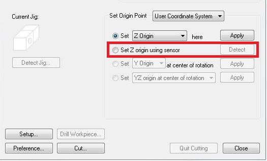
Setting Z origin using sensor
To set the z origin with the sensor, place it under the bit and click on “set Z origin using sensor” and detect :
Using mods
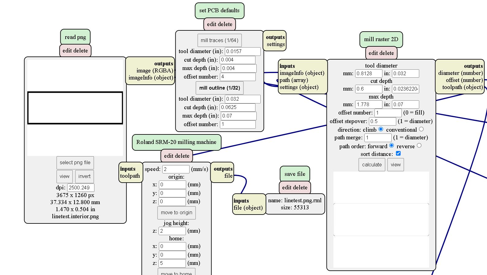
To configure the cutting file, I used mods with the help from this youtube tutorial from fablab Aalto.
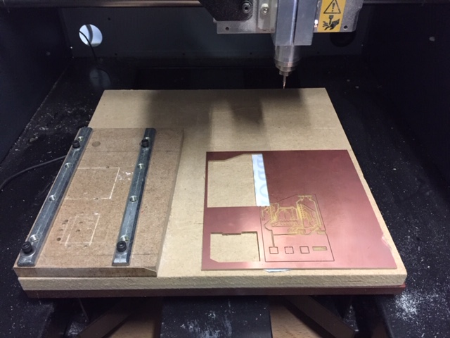
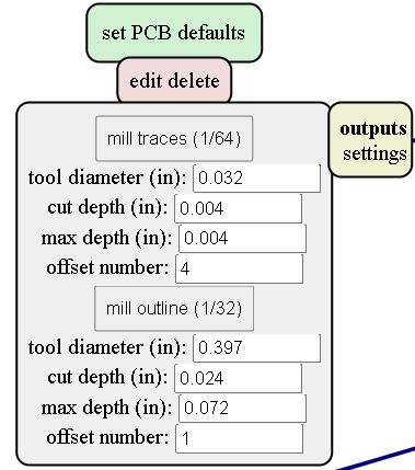
To get into the good mod : right click -> programs -> open server programs -> Roland SRM-20 / PCB png. Here is the setup I used for the first attempt :
Here is the result I had :
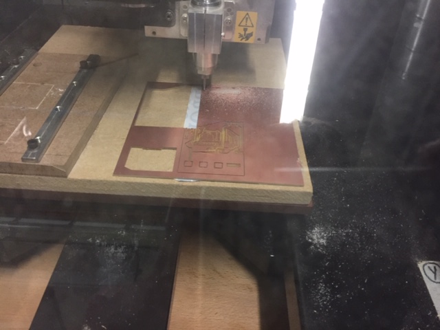
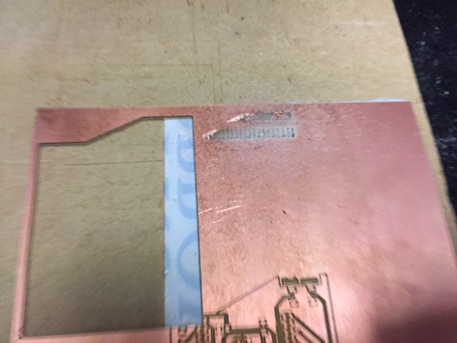
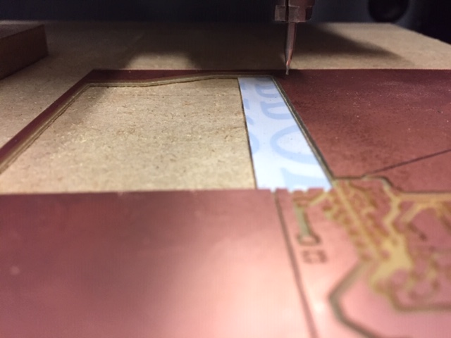
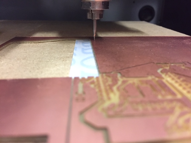
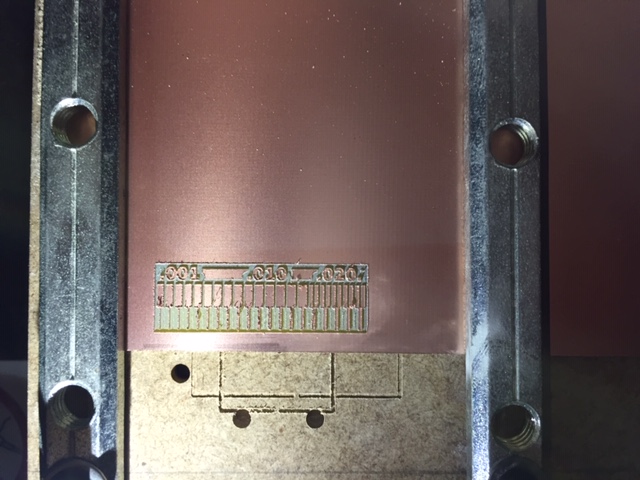
Two problems : I used the wrong bit and the PCB is not plane. So I changed the bit from a 0.062” (1.6mm) to a 0.4 mm (0.0157”) one. And I added extra tape to make the PCB plane :
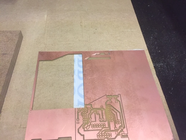
Still not plane. So I used a small device made by a previous fablab user to fix the PCB on the sacrificial layer :
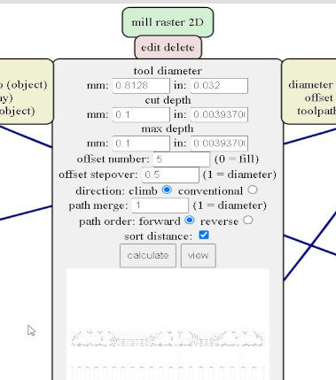
After checking the specs of the FR4 material, 1oz copper cladding correspond to 0.035 mm depth. 0.1mm should be good but maybe my z-height setup wasn’t precise enough. So I changed from 0.1 mm to 0.25 mm cut depth :
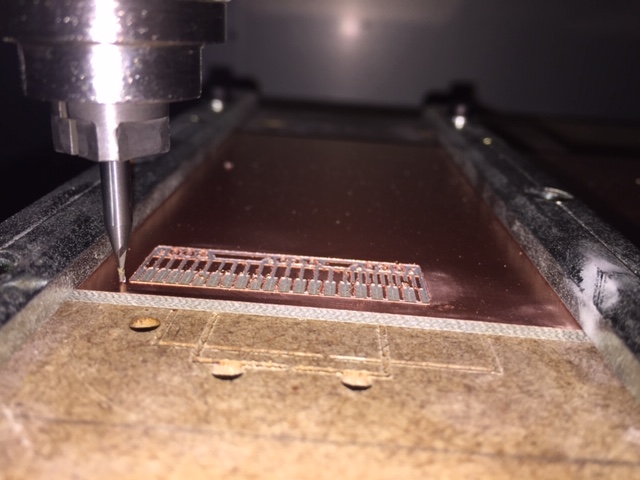
Finally, I cut the exterior after changing the bit for the 0.062” one :
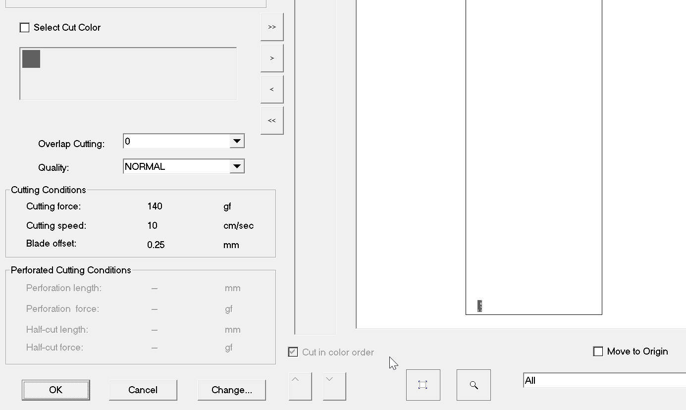
Other PCB process : (Vinyl) cutting
Parameters in Cutstudio. After a few tests, setting to 140 gf worked well :
Removing the copper in excess :
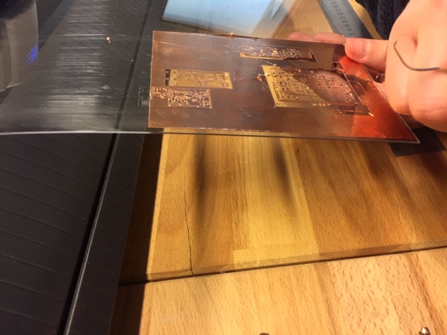
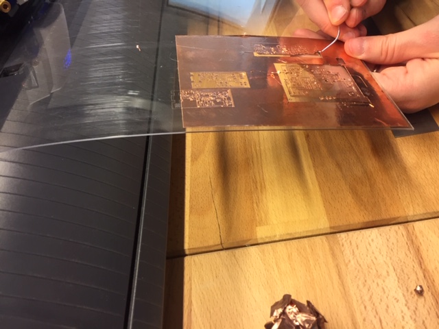
Final look :
We then tried to transfer it to another material but the transfer tape we had close at hand wasn’t working for copper transfer. Our instructor told us afterward that one way to do it would be to put Kapton -which is an insulation for soldering- onto a PETG sheet and then put the copper sheet on top of it. And then, cut directly the PETG sheet (which is also smooth). This is something to try another time.