5. Electronics production
Group Assignment:
Q. Characterize the design rules for your in-house PCB production process; document feeds, speeds, plunge rate, depth of cut (traces and outline) and tooling. ✔
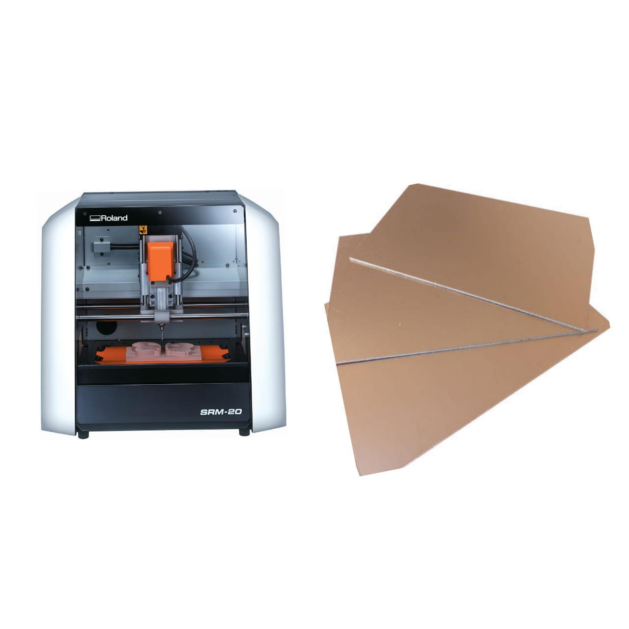
For the Electronic production week we have used SRM-20 milling machine and FR-1 material for the PCB milling.
Before I disscussed about my group and individual assignments, let me take you all through the steps for operating the Milling Machine. - Remove the previously mounted pcb plate if any using the spatula. - Make sure to remove the double tape from the bed completely. - Clean any residues using vacuum cleaner. - Now select the pcb plate( FR-1) and clean it thoroughly to remove dust. - Use double tape to mount the pcb plate on the bed of the machine. - Press gently for proper adhesion. - Used leveling gadget to ensure that the board is leveled horizontally. - Now it is time to mount the drill bit. - To set the drill bit bring the header and the bed area in the center by giving command in mods. - Loose the chunk using L-N key. - Insert the 1/64 drill bit by one hand and tighten it by the other hand.
-
Set the z-axis to a height of 2-5mm above the bed.
-
Then loose the chunk and free fall the drill bit to descend down by gravity.
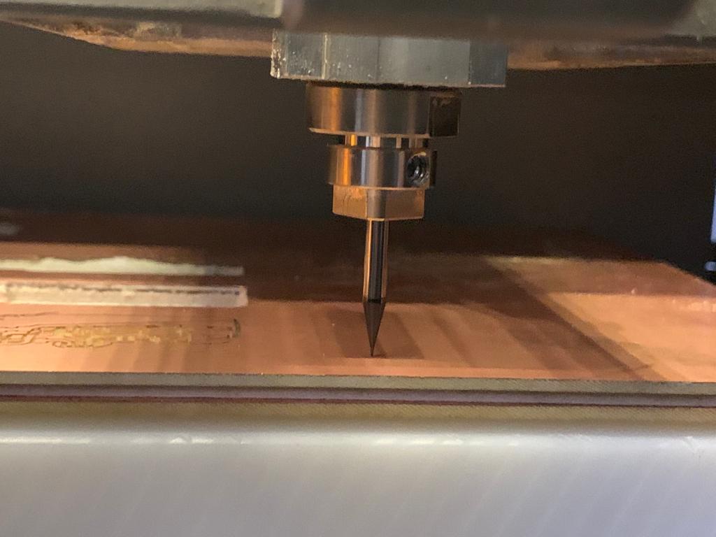
- Tighten the chunk using L-N key.
- Note down the coordinates of the origin.
Generateing tool path using mods.
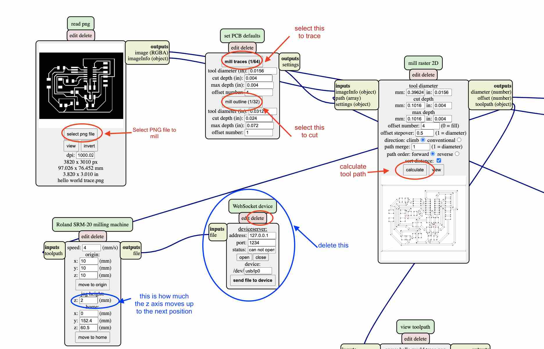
To generate the tool path download the two images of line test and line test interior from the fabacademy website in your desktop or directly to the attached PC of SRM-20.
Now to operate the MODS follow the following procedure. - Open up the MIT MODS website on your net server. - right click and follow this path
Programs -> open server program -> Roland -> SRM 20 -> PCB png
- Select the Photo/Image to be used for milling
- Check the format of the image (.svg or .png) (In my case I have saved the image in .png file)
-
select the drill bit for Cut trace (1/64) and (1/32) to cut the outline of the board.
-
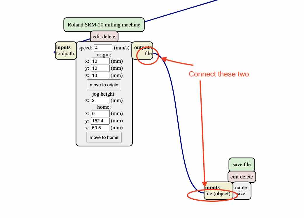
Since the milling machine is not connected directly to Mods, we need to delete the websocket device and add another path to save the file in rml formate. We do this by following this path:
right click -> modules -> open server module -> file (save).
- The rml file generated is then sent to “Vpanel for SRM-20”.
- Make the X,Y,Z coordinates to 0.
- Calculate the path
- Send the File for milling.
PCB MILLING -TRACE AND OUTLINE CUTTING:
For the group assignment, we have downloaded the png files for both the traces and outline form the fabacademy website.
Trace

Outline

For the trace cutting we have used 1/64 drill bit and for cutting the outline boundry of the pcb board we used 1/32 drill bit.
Here are the results.
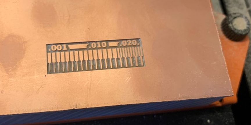
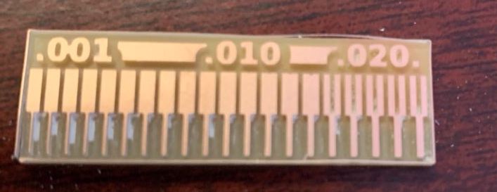
From these assignment we now know that the trace width and the space is only visible properly in the range of 0.020. This is because 1/64 is 0.015 and the 0.02 is the only range that is bigger than 0.015. Therefore, for the future circuit boards, we should stay in this range.
For more details about our group assignment click here
—
Individual Assignment:
Q. Make an in-circuit programmer that includes a microcontroller: mill and stuff the PCB test it to verify that it works
For the individual assignment I have to learn how to mill a In-system programmer and the reason behind of making fabISP is to know how to make PCB board, how solder the components and to understand how fabISP will act as programmer.
To make the In-circuit programmer there are different versions of ISP’s available in the archive. I have selected Brains version (FabTinyISP).
Every details about how to build,program,test and debug the board were given in the archive.
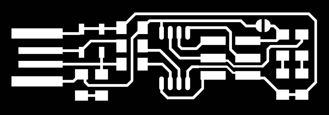
FabTinyISp Milling Traces
 FabTinyISP outline
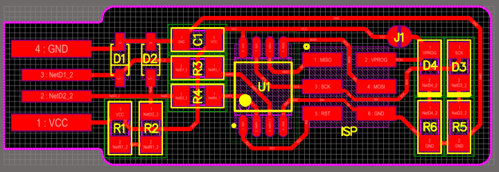
 FabTinyISp Position Diagram
I have downloaded the Trace and Outline image from the website. For milling the PCB traces I have used 1/64 drill bit and cutting the outline I have used 1/32 drill bit. I used MIT MODS to generate tool path as I have described in my above passage.
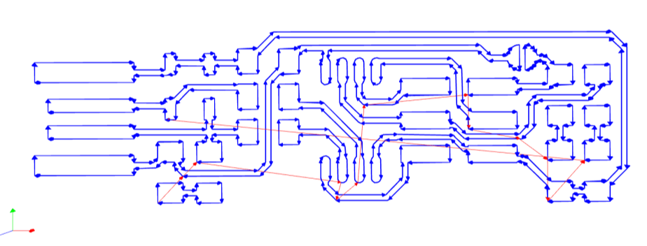
Generated Toolpath.
Steps to Mill Brain’s board.
- CLose the front door of the milling machine properly.
- Power on machine.
- Prepare Vpanel from the desktop from where you wanted to start milling the PCB.
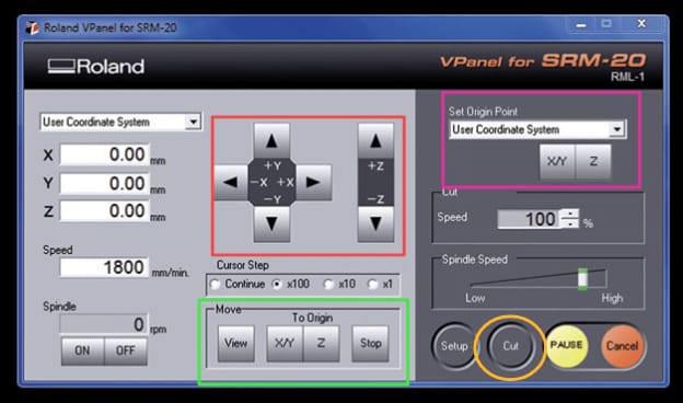
Set user coordinate system according to the space available on the pcb board.(RED rectangle)
  Press X/Y and Z heighlighted in GREEN rectangle, it will take you back to the origin.
  Use gravity fall method to set the Z axis and when the end mills are in the desired positions, press the Set Origin Point heighlighted in the purple rectangle.
  Then, press on the cut button by choosing your file and press add.
THE FABRICATED BOARD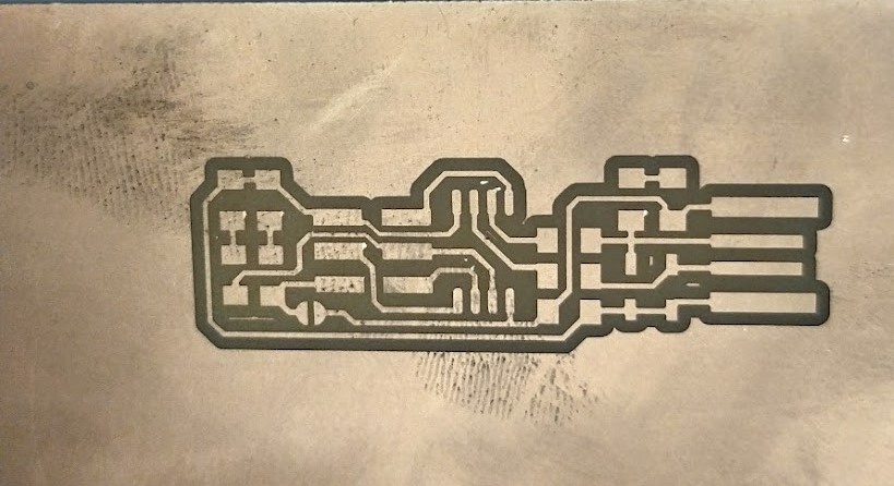
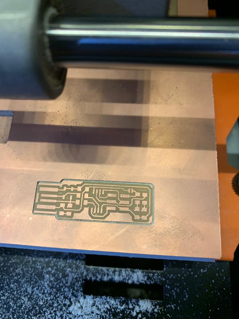 Clean the bed and the board with a vacuum cleaner after completing the milling.
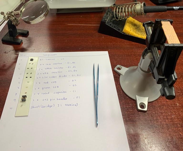
# Soldering the PCB The very first step before soldering is collecting the components. The best thing is stick the components against a list of components written in a sheet of paper. I have used a single sided tape to stick components to the paper. The tape will keep the components in place and it will reduce a lot of confusions in future.
 Me trying my best to soldering the components.

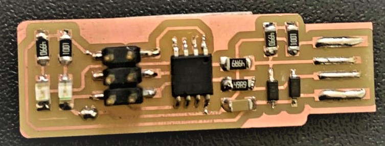
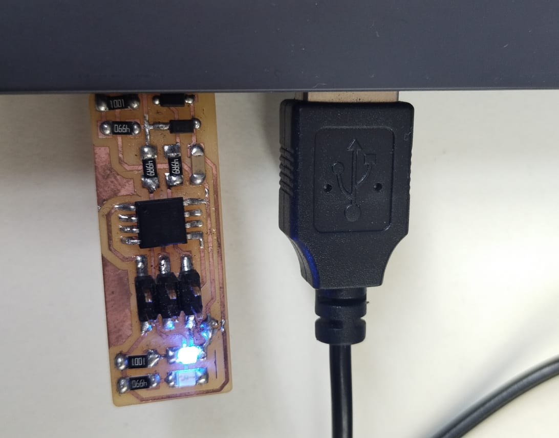
MY SOLDERED ISP BOARD.
# Programming FabISP Board Before programming the board Look carefully at the board to see if all the components are connected properly. To programme the FabISP, all the detail procedures were given in here
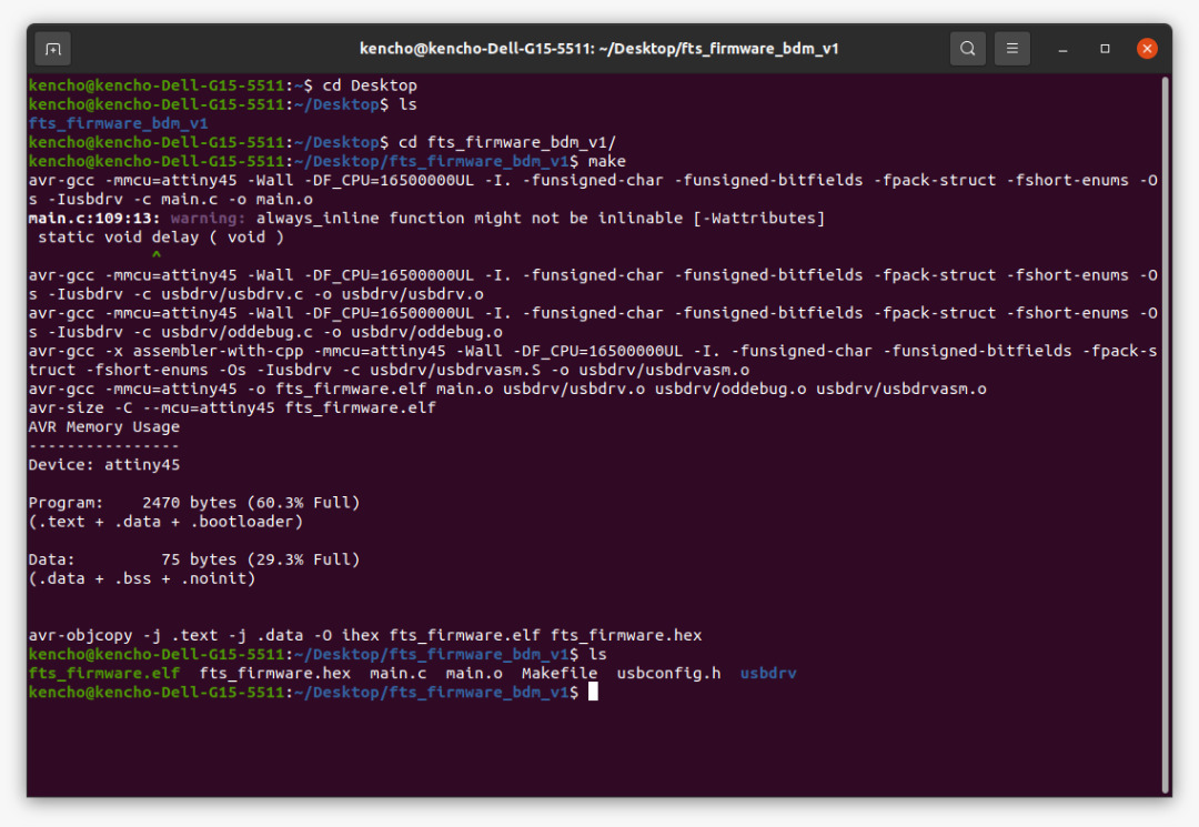
I programmed my board ISP using Ubuntu.
STEPS I followed to programme my FabISP.
- Downloaded the firmware sourcecode and extracted the zip file.
- Opened Ubuntu terminal and ran cd to view the directories.
- Ran make. A file called fts_firmware.hex was generated.
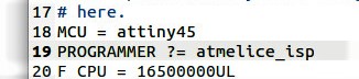
- Opened the makefile in Notepad++ to change the PROGRAMMER ?= usbtiny to PROGRAMMER ?= atmelice_isp.
- I plugged my board into a USB port and blue led blinked, it means my circuit connection is good.
- Then I connected the programmer to my board through ISP header. (Note: Make sure to place the pins correctly with the help of the PIN number 1 marker).
- Ran make flash. This will erase the target chip and program its flash memory with the contents from the .hex file you built before.
- You will see several progress bar while avrdude erases, programs, and verifies the chip.
- There are no errors so, I ran make fuses command. This will setup all the fuses except the one that disables the reset pin.
- Before blowing up the fuse that will enable it as programmer, it is recommended to check the USB functionality. Therefore, I did unplug my board and the programmer.
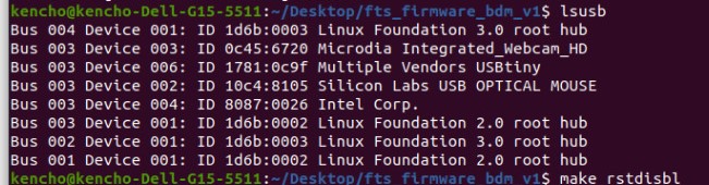
- Then plugged back my isp board and ran lsusb command in terminal.
- Multiple vendors USBtiny was displayed, which means my programmer is ready.
- FINALLY, I blew up the fuses and made my programmer ready.
Learning outcomes
- Learnt how to use SRM-20 milling machine
- Learnt how to prepare Vpanel from desktop
- Learnt how to use MIT MODS.
- Learnt how to make a in circuit programmer.
- Learnt how to use ubuntu
- Learnt how to do soldering and Introduced to different electronic components.
THANK YOU