2. PCB
When I started working on the final project I tried to imagine how to split the functions of my projects and think about the data flow. That lead me to the following chart.
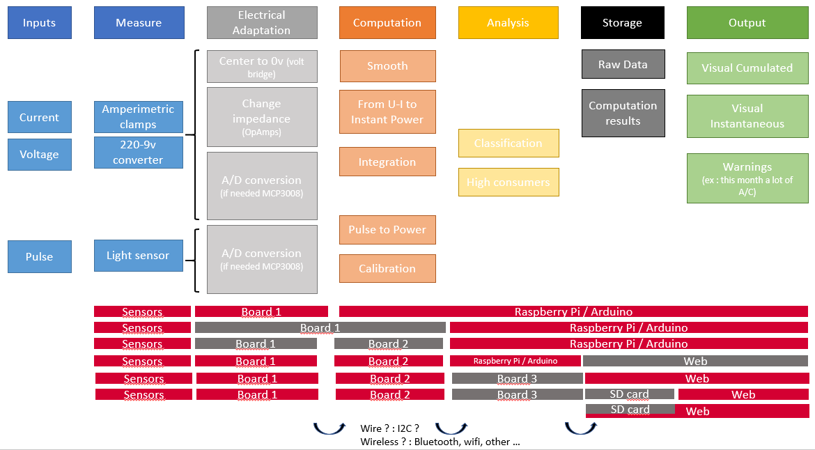
Then taking into account what I learnt during the Input week :
- I will use Emonlib_CM on an ATMEGA328p
- The ESP32 does not have a good ADC
- Transferring EmonlibCM to the ESP32 is not an easy task
I wanted to put all the microprocessors on one board but it got messy really quick. So talking with my instructor and answering the following questions :
- Is it reasonable to have 3 microcontroler in my project ? --> Yes
- Communication I2C (ESP32/ATMega1/ATmega2) --> It is fine
- Powering ? Flash, serial, 230V --> Can be done
- Flash ? how to manage two SPI ports on the same board --> I must have one per Atmega
- Can I remove the FTDI ? --> Yes
- Can I share crystal between ATmega --> No
I decided to make a specific “EmonLibCM” board for data reception/analysis. EmonlibCM is the library developped by OpenEnergyMonitor that runs on the Atmega328p.
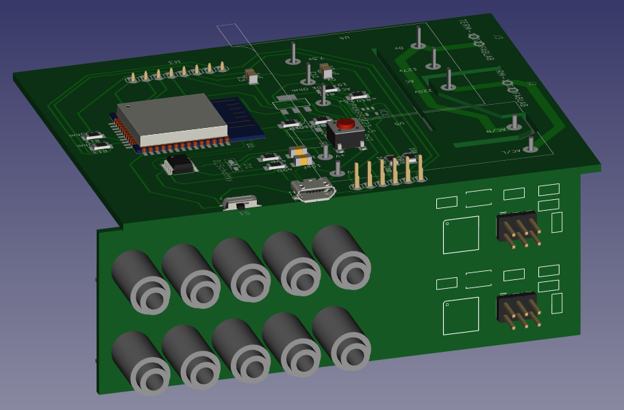
Finally my layout will be as follows
- LuzMon : The main board receiving the ESP32 and the PowerElectronic
- JackBoard : the board receiving the current sensor jacks and the ATmega for signal analysis. There is two of them to make it modular.
- LuzDisplay : the board that make the bridge between LuzMon and the OLED screen. It also contains 3 push buttons to control the screen
Info
I added the buttons following the advice of my instructor. He explained my that when you have a screen meant to show complex data it is interesting to have 3 buttons. 2 to move in menus and 1 to validate. I am not sure yet how I will use them but they are here.
LuzMon
LuzMon is the board that will be the conductor of all the boards of the project. It’s role will be to :
- Do the Power Conversion from 220V to 5V to power the boards
- Do the Power conversion from 220V to a signal manageable by the ATMEGA ADC
- Request or receive the measured data from the JackBoard via I2C
- Send data to be displayed on the OLED screen via I2C
- Send data via Wifi to the RaspberryPi
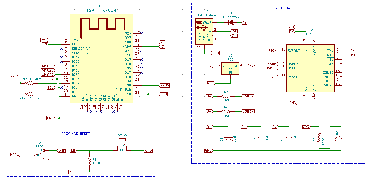
Schematic
To comply with the requested task for this board, the main components I had to install on my board are :
- ESP32 using the Barduino design
- Power Source : 220V - 5V - 2A
- Voltage transformer : 220V - 7.5V
- FTDI Chip to flash the ESP32
- OpAmp in votlage follower mode
- Pins for connection
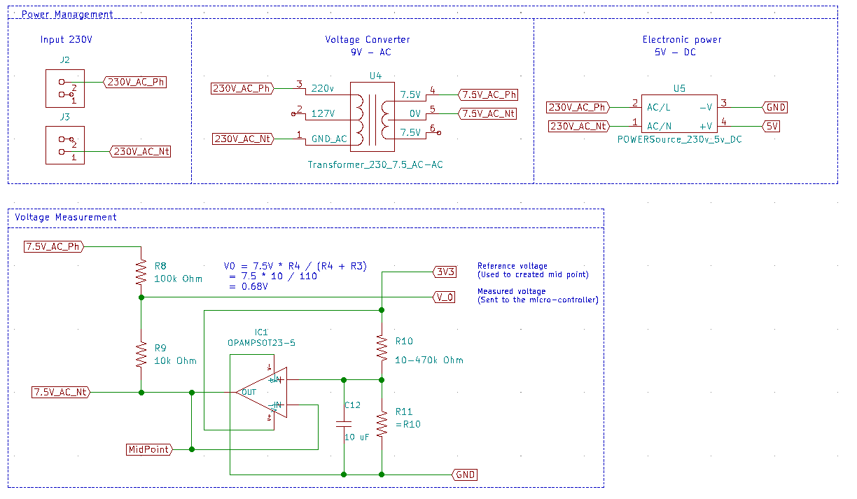
Powering the board
To power the board I used what is called a Power Source which is composed of :
- a voltage transofmer (coil)
- a set of diodes to have only positive values of voltage
- capacitors to filter the signal
- a voltage regulator to have the desired voltage ouput
Measuring 220V
All the theory used for this part and the hardware used is explained in my Input week Theory of Voltage sensing.
I2C network
To have my I2C network I installed to 10kOhm pull-up resistors on the SDA/SCL lines.
At first I did a mistake by using pins 22 and 21 (SD0 and SD1) of the ESP32 for the I2C network but those pins cannot be used. So I prepared a new board design using GPIO 27 and 26.
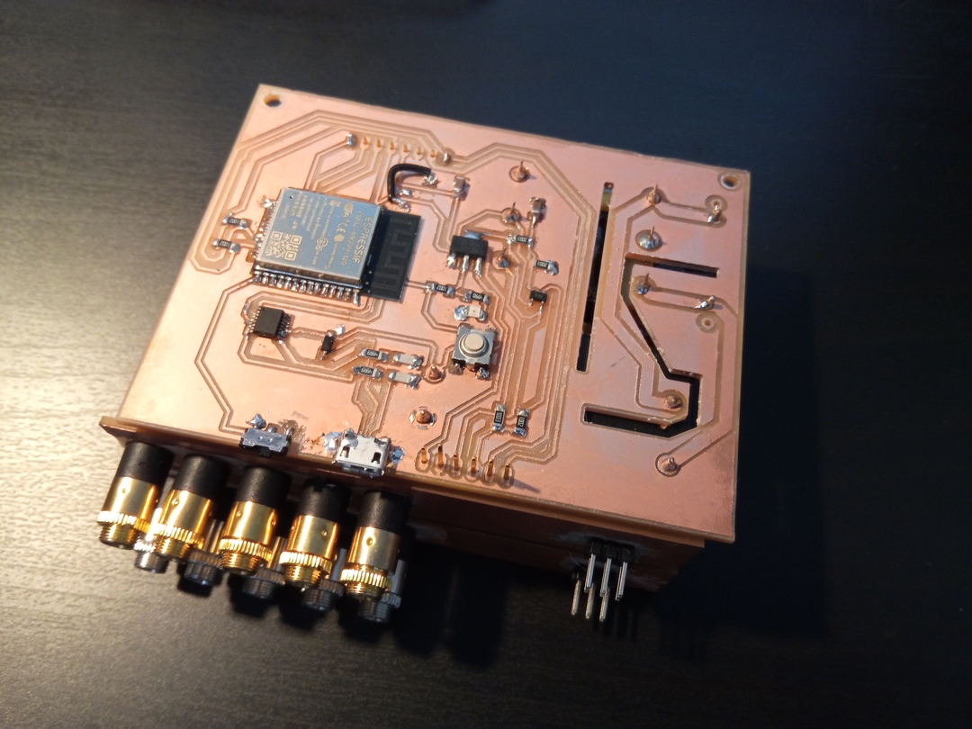
WIFI
The wifi communication will be done through the ESP32. The requirement for a good WIFI signal is to have the antenna of the ESP32 outside of the PCB or at least without copper underneath. In my actual design none of the above mentionned condition are respected but in a next release I will improve this point.
Final Design
The application of above mentionned principles gave me the following schematic.
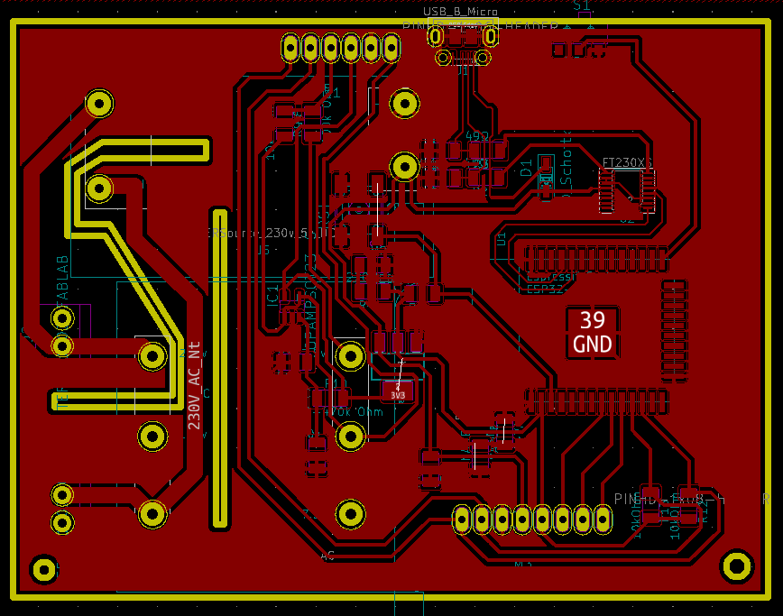
PCB
Once the schematic was done the routing was another intersting job …
The main points of focus were :
- Fitting the components … of course
- Thinking about connections with other boards
- Space management
- 230V management
- I2C network quality
It has been a hard job but I finally reached the following design. One can notice the air gaps to isolate the two 230V tracks and also to isolate the High voltage from the I2C network to avoid perturbation.
I also made the whole plate to be as “Ground” to improve even more the I2C quality because the ground part will absorbe more electromagnetic pertubation.
In an ideal case it is a good idea but in a practical application I did not like it because it makes each short much more problematic and easy.
Also to avoid using a two sided copper board I used 0 Ohm bridges.
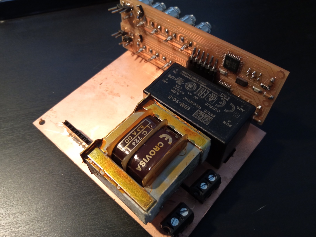
Production
I had a lot of issue producing the board because I had a rough finishing effect. After several test I came to the conclusion that my end mill came to the end of its life. And changing it changed the game and I could get the desired quality ( I forgot to make a picture …)
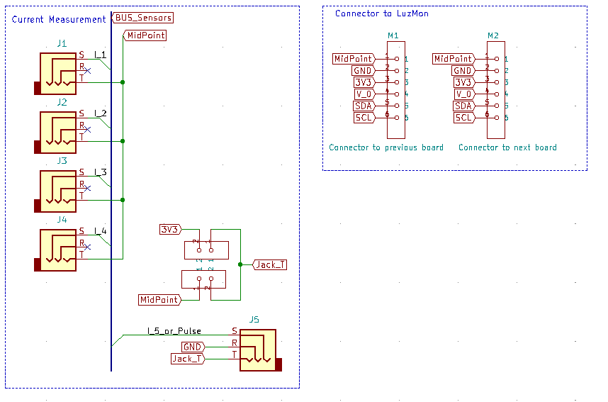
JackBoard
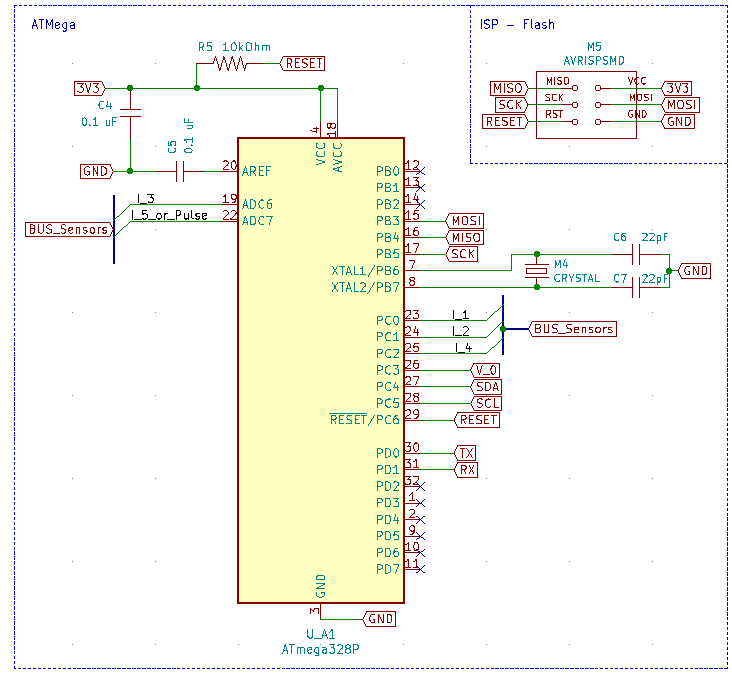
The JackBoard is a direct application of the OpenEnergyMonitor design but adapted to my requirements. So I mainly used the setup of the Atmega328 and the rest is of my design. The main tasks for this board are :
- Connecting the ATMEGA as in the EmonPi design
- Power
- 16Mhz Crystal
- SPI connection for flashing
- ADC connected to Current sensors and voltage reference
- ADC ref connected to ground ADCref = Vcc.
- Receiving the jacks connector of the current sensor
- Receiving the pins from the main board
- Sending information to the next JackBoard
- Be modular, several boards of the same type can be added on the top of each other.
To proceed to the design I used the ATMEGA328 datasheet available here.
Schematic
In this case the schematic was not too complicated. I will mention two points of interest.
AREF
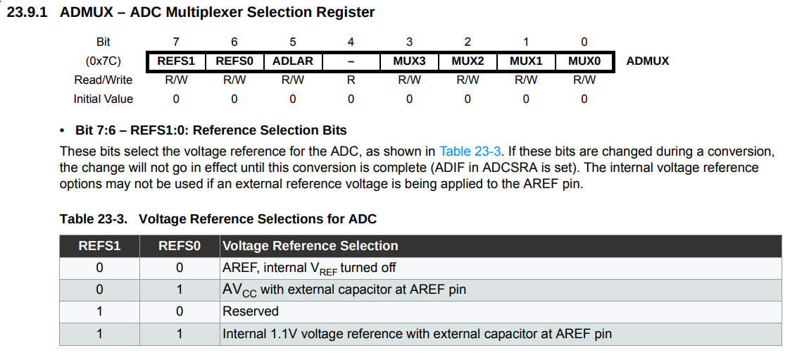
In the Schematic of the EMonPi, AREF is connected to ground. The AREF is the voltage reference that will be used by the ADC to evaluate the voltages on its pins. So it was not normal in my opinion to have it set at 0V. But by reading a bit more on the subject in the datasheet, I found out that you can set the Atmega to use AVcc directly instead of the AREF pin by checking to things :
- AREF pin has to be connected to GND via a capacitor
- The register ADMUX has to be set to bit 7 = 1 and bit 8 = 1 as shown in the follo
This is shown here in the datasheet.
So this is done via the GND connection and the two lines of code from EmonlibCM.cpp
72. #define VREF_NORMAL 1                // ADC Reference is Processor Supply (AVcc) (from EmonLIbCM.h)
98.  byte ADCRef = VREF_NORMAL  << 6;                                       // ADC Reference: VREF_EXTERNAL, VREF_NORMAL = AVcc, VREF_INTERNAL = Internal 1.1 V
932. ADMUX = ADCRef + ADC_Sequence[next];     // set up the next-but-one conversion
Jumper
I installed a jumper that routes either 3.3V or MidPoint to the Jack_T flag. It allows the user to choose what will be the use of the last jack connector of the board.
- Jack_T = 3.3V : the connector will be used for the pulse sensor
- Jack_T = MidPoint : the connector will be used for a current sensor.
Final Design
This taken into considaration I reached the following schematic.
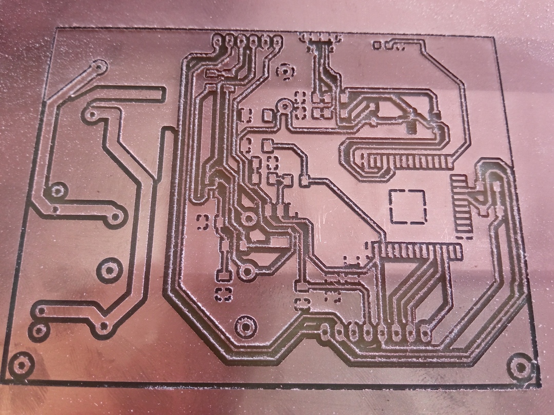
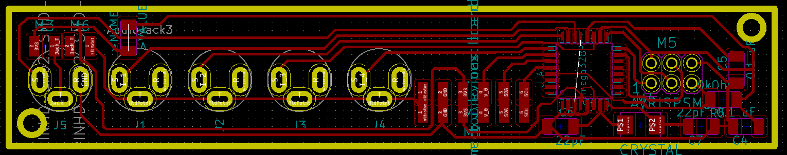
PCB
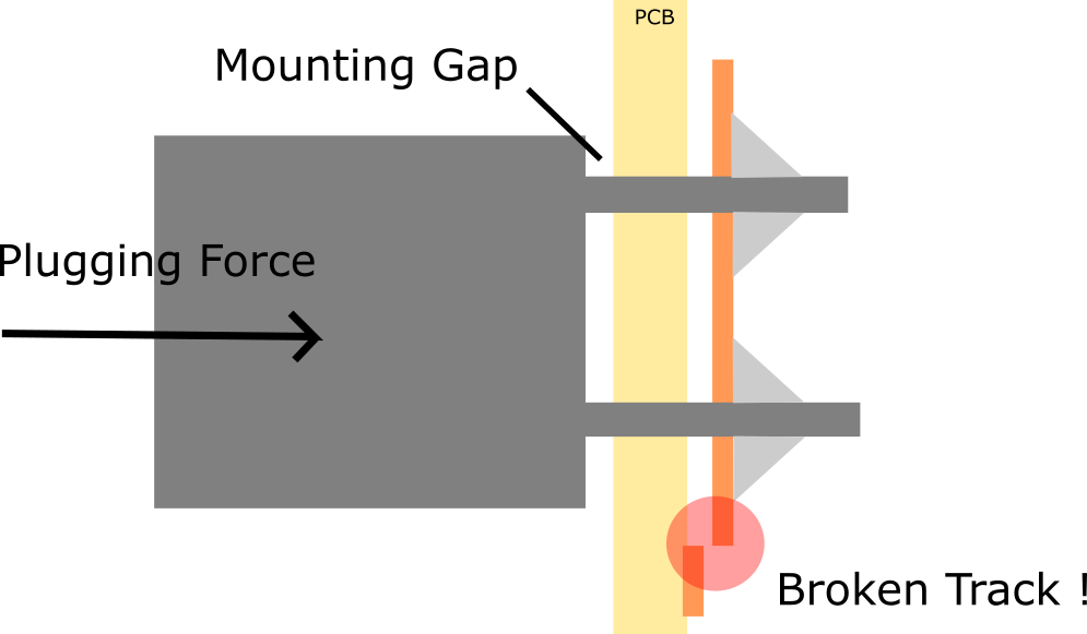
The PCB design has been really complicated due to the space management. Indeed the total height within the casing was restricted due to the fuse-box in which it will be installed. This lead to a maximum height of 16.5mm. To do so I had to use thin traces (0.2mm), which is ok in terms of supported current but no so good in terms of board durability.
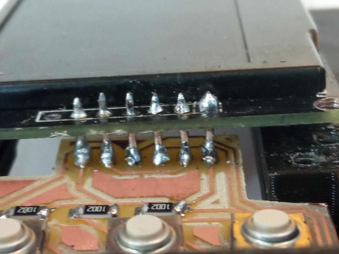
Another hard point I hit is that when I soldered the jacks connectors they were not touching properly the PCB and the “plugging forces” hold almost entirely on the tracks. This provoked one track to break under the stress.
Another point to take into account is the way boards will be connected on the top of each other. I had to be sure that adding the pin connection would not make the final PCB bigger than what the casing can hold.
This was checked via a common work between PCB design and Casing design using the capacity of Kicad and FreeCad to work together exchanging 3D models.
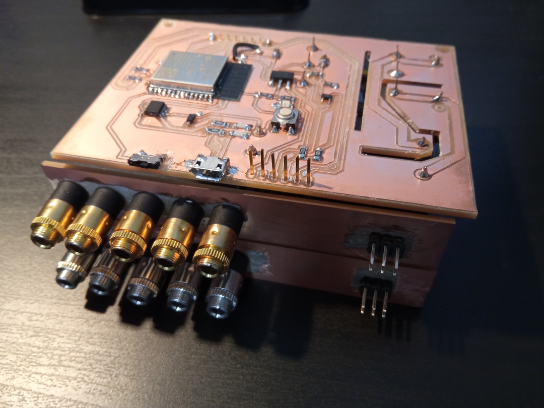
And here is the final PCB design.
Production
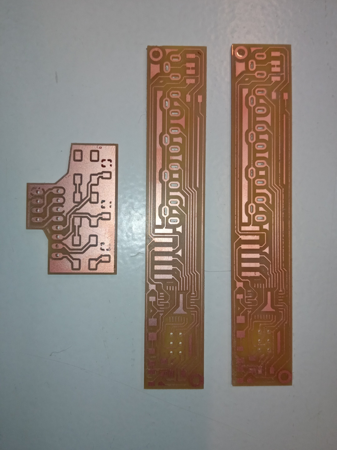
The production went pretty well thanks to my new end mil.
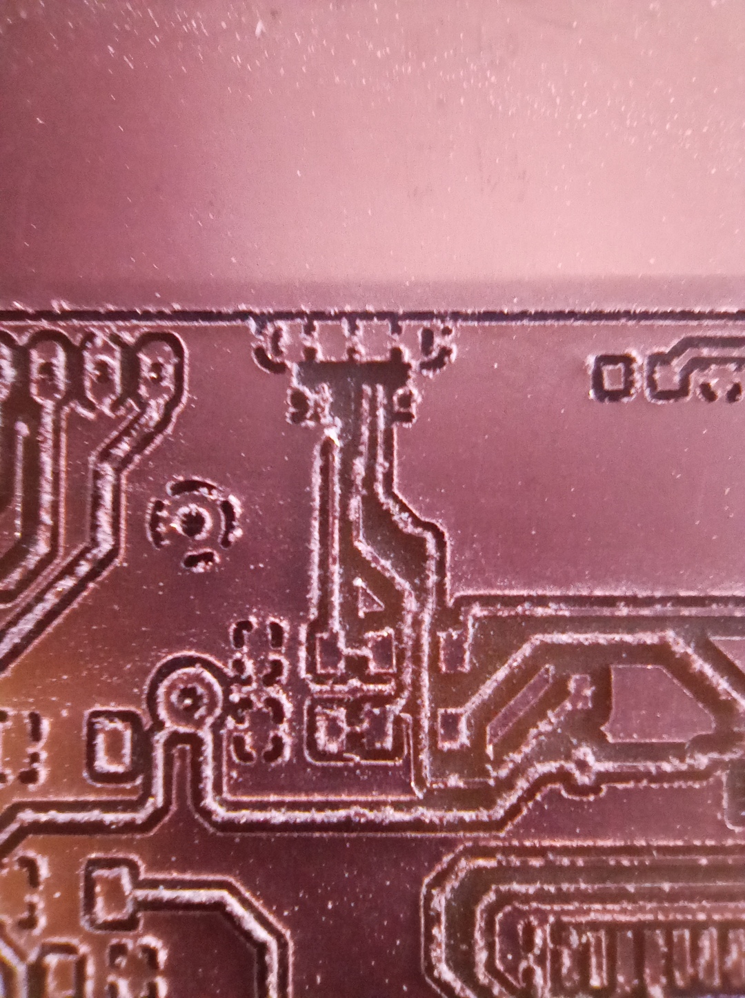
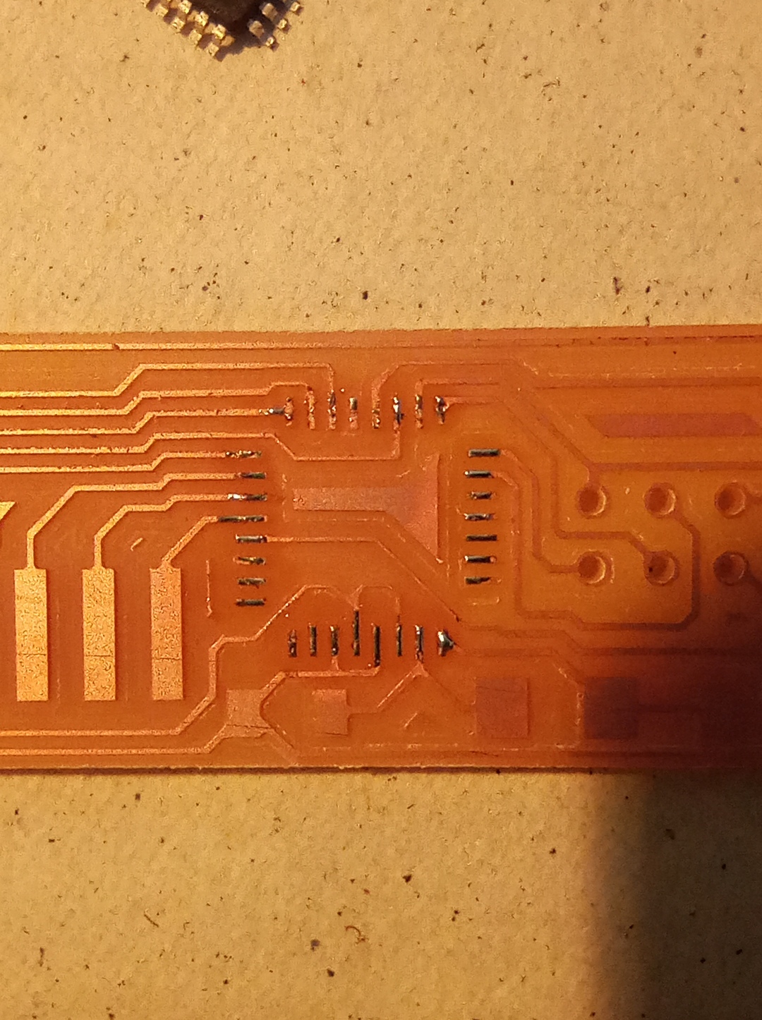
Here is the board milled (alongside the LuzMon Display which is commented in the next section)
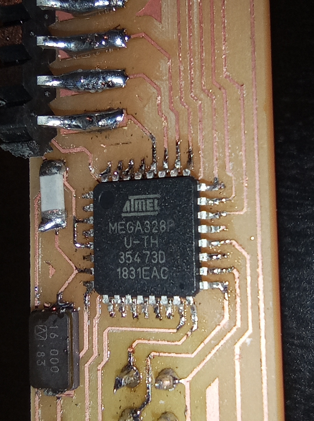
Soldering was another game ! I used the following technic to be sure that all pins of the ATMEGA would make proper contact. I lay a really thin (as less as possibl) layer of solder on each pach.
Then I placed the ATMEGA on its pads and heated up each pin with the soldering iron. It worked like a charm !
LuzDisplay
This board is here to :
- Make the connection between LuzMon and the OLED screen
- Host the three command buttons of the screen
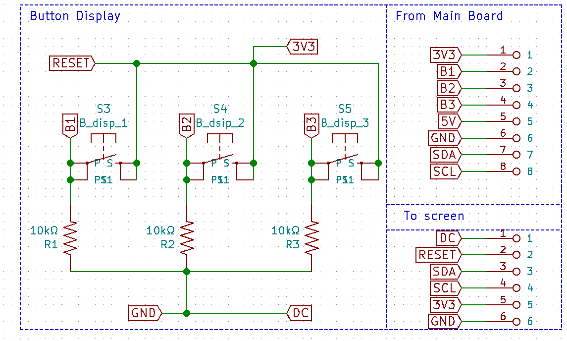
Schematic
The important points of this board is to have the pull-down resistor for each button and to route properly the connections of the OLED screen.
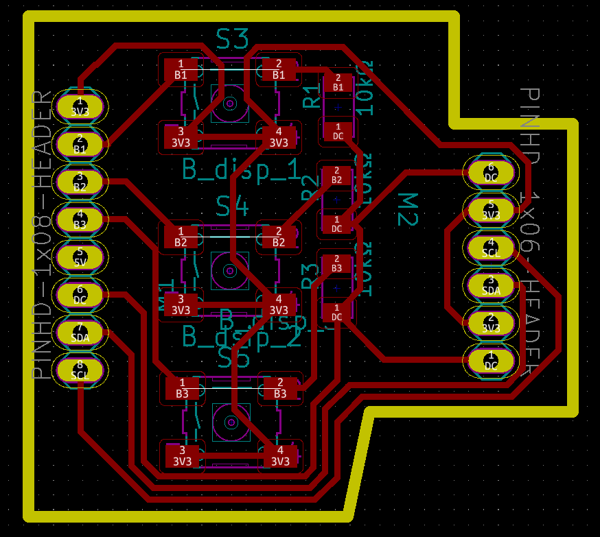
PCB
The PCB was also prepared in close relation with the 3D model of the casing to properly fit within the upper part and also to have a proper contact with the buttons.
Production
The milled board is presented in the same picture as in the previous section. THe milling when without major issue.
The only “complicated” point is that the soldering pads of the board and the screen are on the same inernal side. But has some space has to be left for mounting purpose it was not an issue.
Final assembly
Here is the 3D model of the assembled PCBs that I used to evaluate the space occupation.
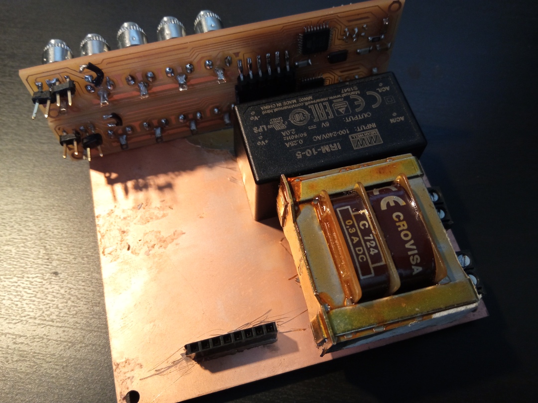
And here is the final assembly of all the boards and components.
Bill of materials
The Bills of material was generated using Kicad in CSV format then adapted to ODS format.
Improvements
- Remove copper below ESP32 antenna
- Avoid mechanical effort of the boards especially due to the jacks
- Through hole connectors for interboard communication
Files
- LuzMon - main board
- JackBoard - current sensor board
- Display - board for buttons and OLED Screen
- Light pulse sensor