4. Electronic production
Group Assignment
The group assignment was the occasion for :
- Learning the software and hardware to be used for electronic production
- Learning the limits, advantages, disadvantages of the processes
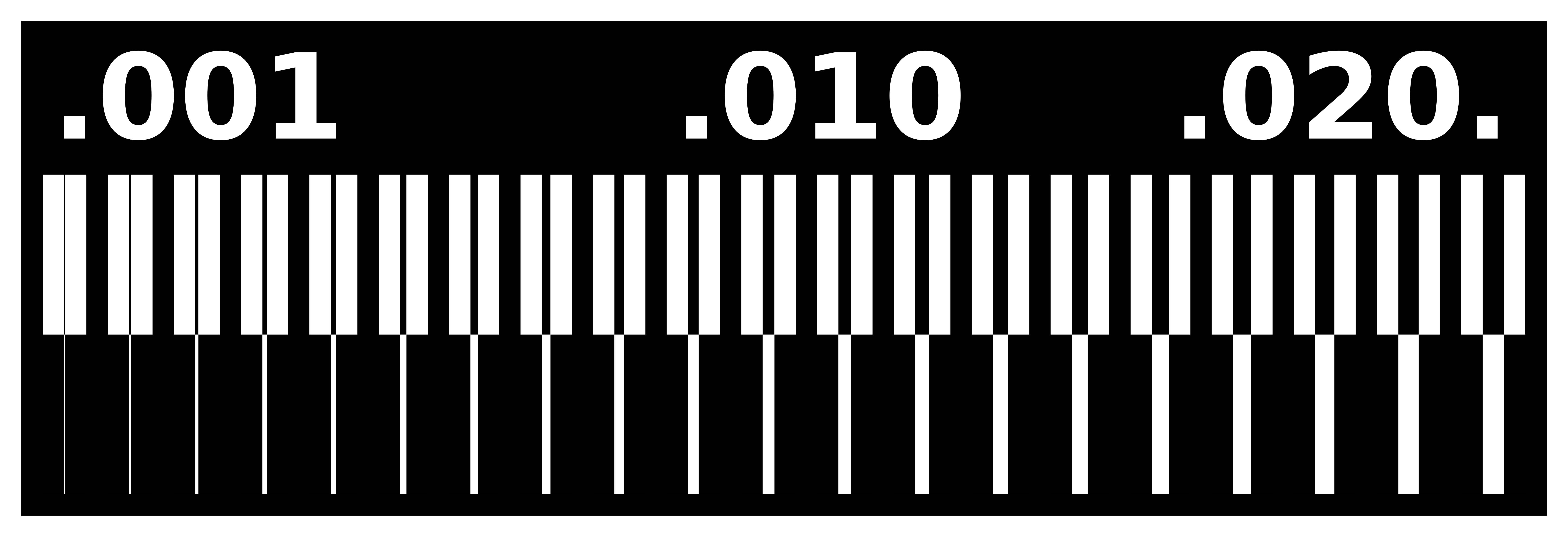
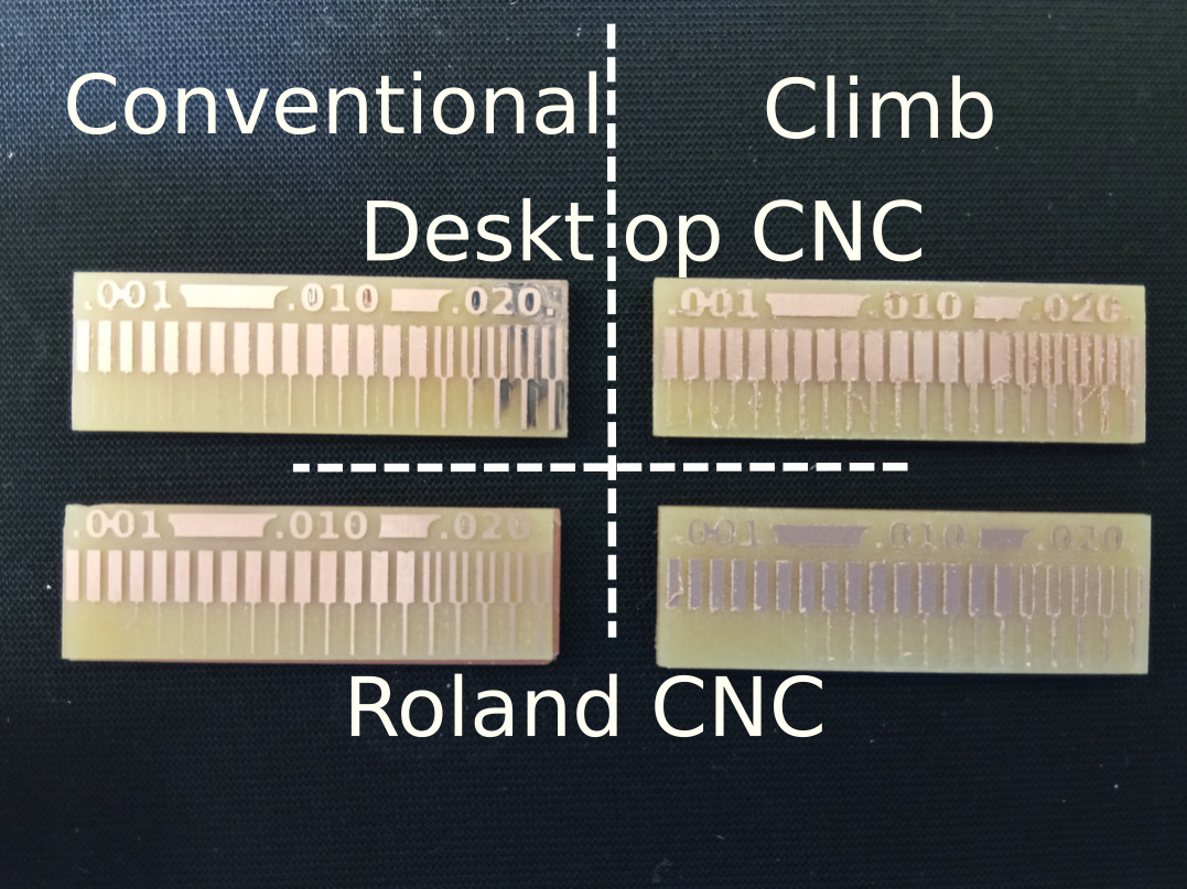
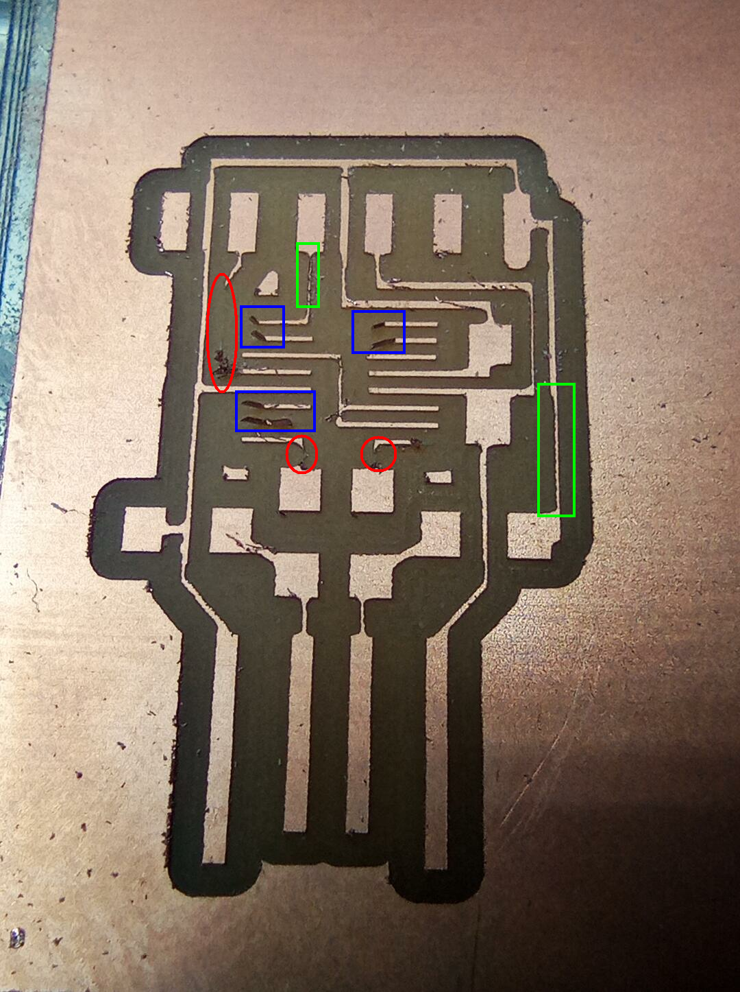
The PCB below is a test to evaluate how precise our tool can be and the size of the traces we can make.
For this assignment the main variables we had were :
- The machine : Roland or Desktop machine
- Climbing or Conventional
- Linear speed of the tool
Before starting
- Be sure to fix properly your plate on the sacrifical plate
- Check your units !
- Run a milling “in the air” if you have a doubt
Here is the result of the tests conducted.
Conclusion
From the group assignment we learnt the following
Conventional vs Climb : conventional rotation gives a clean job; the traces are clean. But the drawback is that the traces are much thiner than with the conventional. As you will see for my assignment; I started with conventional but the traces were torn appart from the plate. So I had to go for the climb option.
Limits
As we are using a 1/64 in. tool the minimum space between traces is fixed and of 0.015in ~ 0.4mm and we can see it on the image above where the traces have not been created.
The minimum width traces seems to be around 0.09in ~ 0.23mm, that is because below this threshold the traces are torn appart by the machine. If you have the space on the board, I recommand bigger traces because they are less fragile.
Assignment
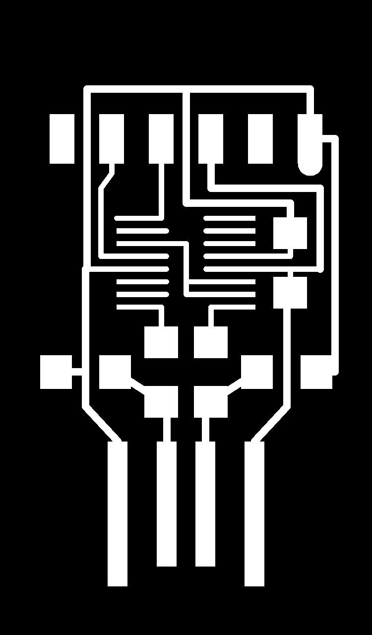
The assignment consist in milling, stuffing and testing a USB-FTDI-UPDI board. I will present each steps I have been through and the difficulties I had.
Milling
Preparing the files
To prepare the files I ran into a small issue with Mods. Indeed if the png file of the trace is to heavy, it eats-up all the memory of the Pi and the NC file cannot be created. I made the test with Fab Modules and I had no issue. Mods can be used but the files have to be rescaled. Mods : http://mods.cba.mit.edu/ Fab Module : http://fabmodules.org/
Here are the steps I followed on Mods to create my files.
- Go to mods with your favorite browser : Mods
- Basic commands
- Left click : move the window
- Right click : pop-upo menu
- Mouse wheel : zoom
- Basic commands
- Click in the white area and select the following menu
- Programs -> Open server programs -> Roland MIL / SRM20 / PCB Png
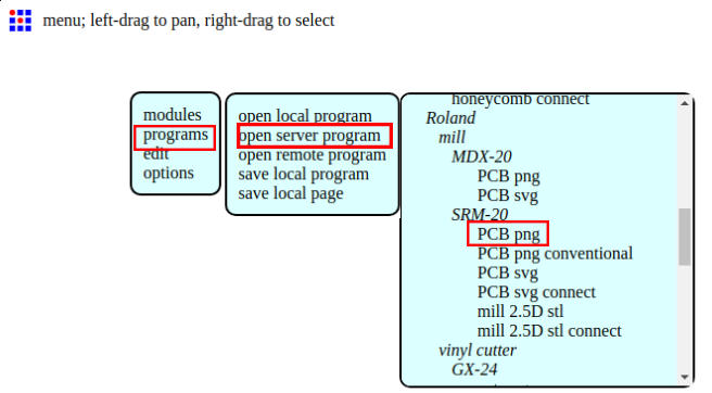
Opening the Trace tool from MODS
- Programs -> Open server programs -> Roland MIL / SRM20 / PCB Png
- The global view of the tool is as follow
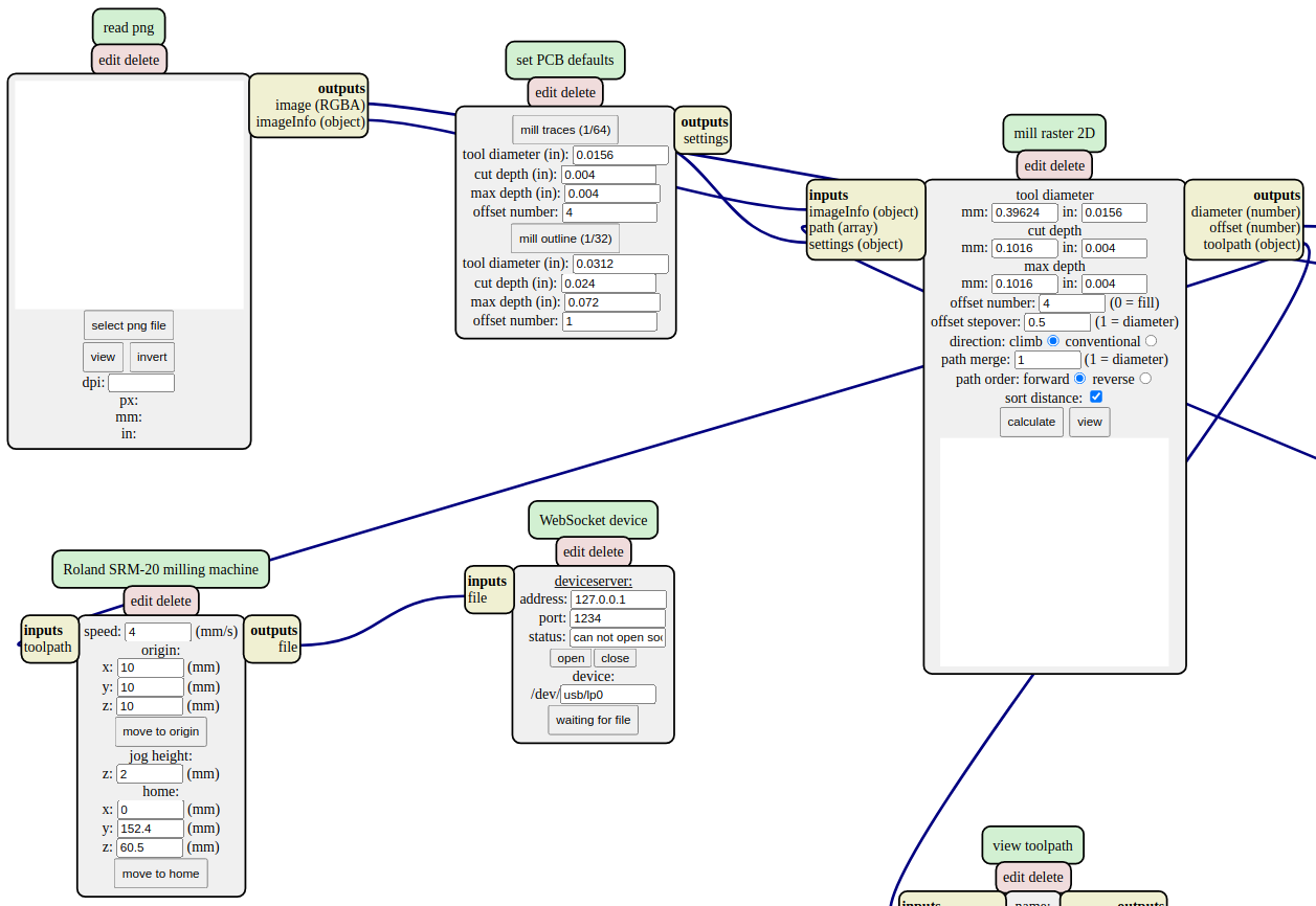
MODS Global View
First step is to choose the PNG file (click “Select PNG File) of the board to mill. Either the traces or the outline to cut. Check that :
- The file is the correct one
- The part to be removed is black
- The size is the expected one
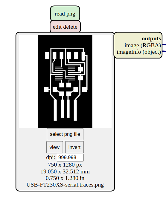
For traces : Mil Traces (1/64)
For cutting : Mil outline (1/32)
The number is paranthesis corresponds to the tool diameter in inches.
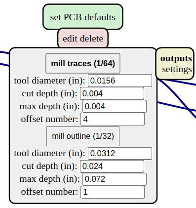
Once you have select the correct cutting type, most of the parameters will be correct as default.
- tool diamer : comes from the previous window
- cut depth : how much of the material will be removed vertically / step
- traces : 0.1016mm to remove the copper only
- outlines : 1.8297mm to remove copper and PCB base
- max depth : how much of the material will be removed in total
- traces : same as cut depth, it is done in one step
- outline : 3 time the cut depth, it will be done in 3 passes
- direction :
- choose either climb or conventional. Usually climb gives better results
- Rest of options :
- Leave a such
Here we set the following info * Horizontal speed : * Traces : 3mm is fine * Outline : < 1.5mm/s to avoid breaking the tool
Some machine take the speed as mm/mn !
- Origin : is where the machine will start milling based on its own origin
- Jog height : is the altitude at which the tool moves when not milling
- home : is where the tool will go once the job is done
- important to set a high Z to avoid scratching the PCB
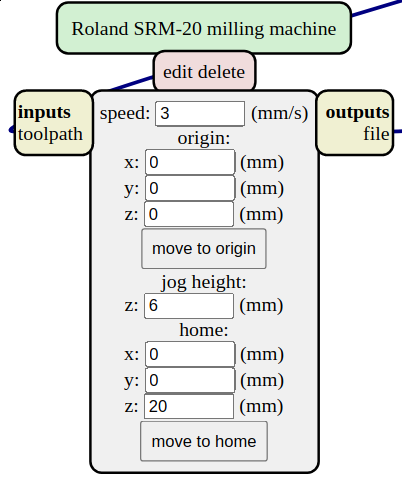
- important to set a high Z to avoid scratching the PCB
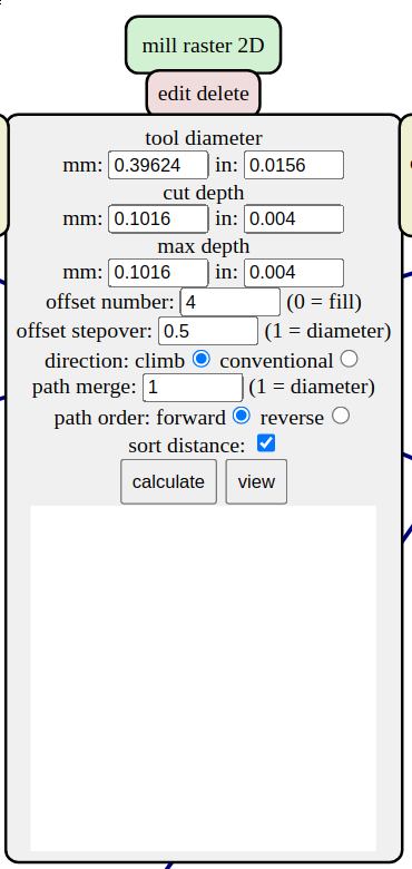
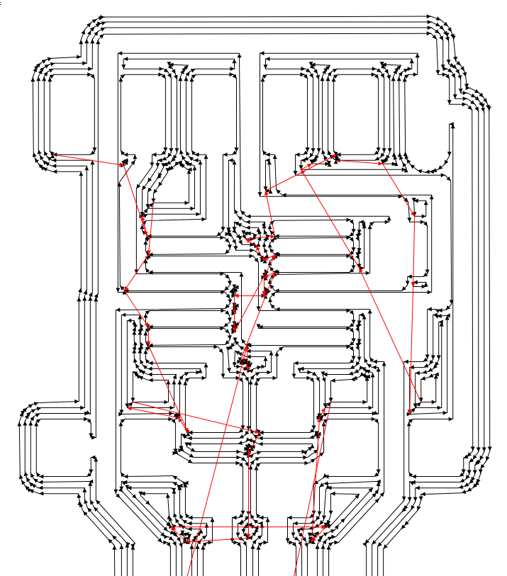
- Click on calculate and the trace will appear in the window below.
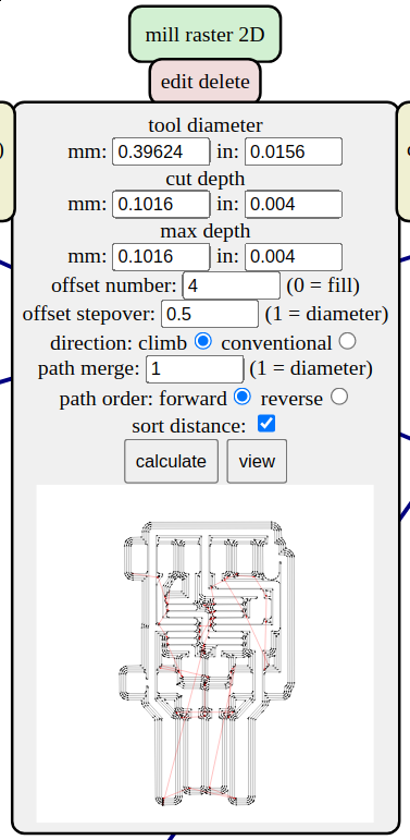
- Click on view to be sure that the tool does the expexted job. It should
give you a “clean” result and be sure that all you traces are present.
If you give not enough space between traces then the tool cannot pass and
the trace will be ignored.
Set-up
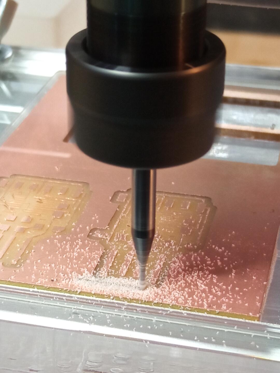
I milled on the desktop machine using Candle and my Raspberry Pi. Candle worked pretty fine and is intuitive. Below one can see the milling of the USB-Serial board on going.
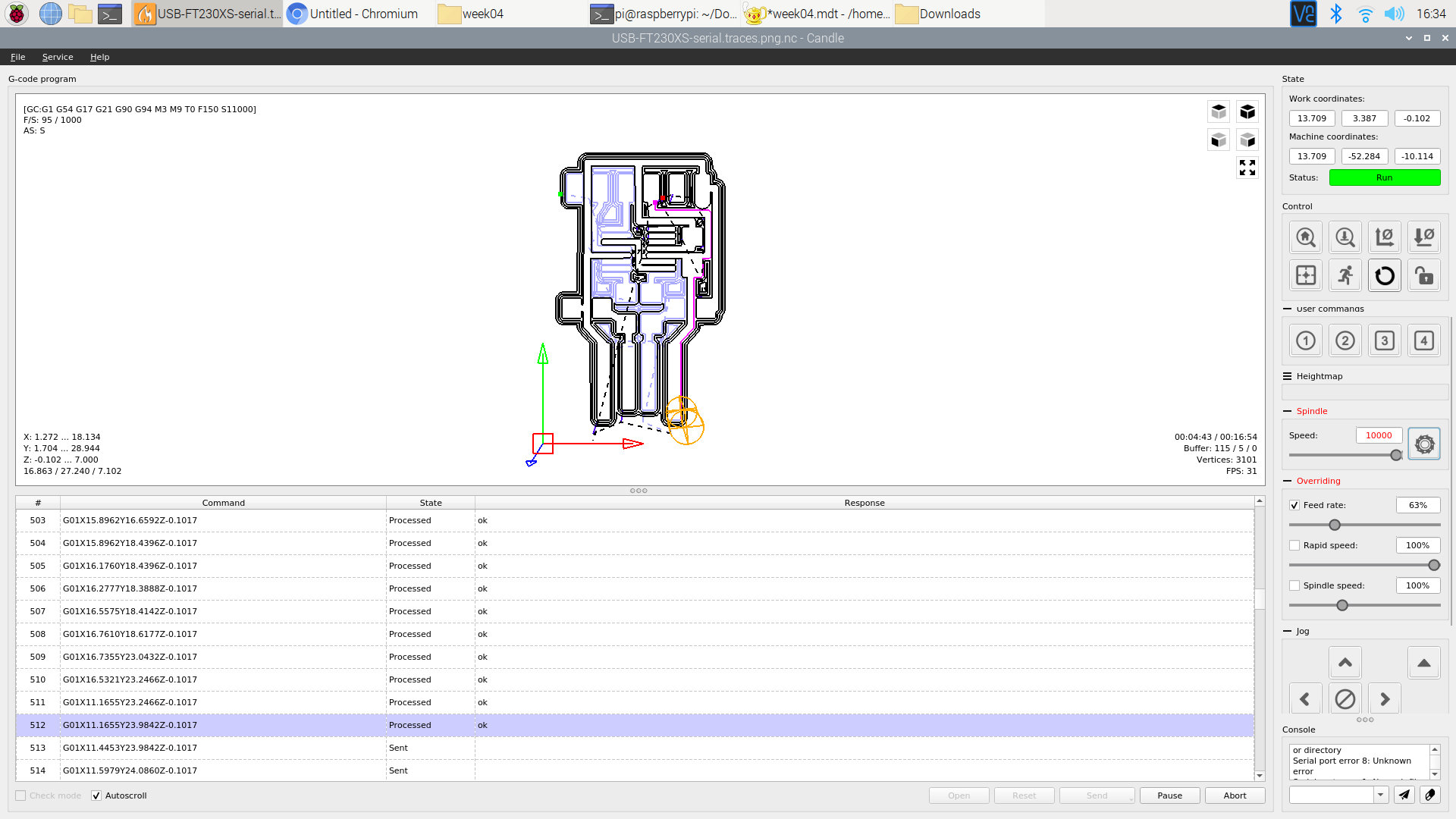
Candle worked without incident related to the Pi. It is not to demandeing and the Pi supported it pretty well even the milling animation. I installed Candle really easily with the command :
sudo apt-get install candle
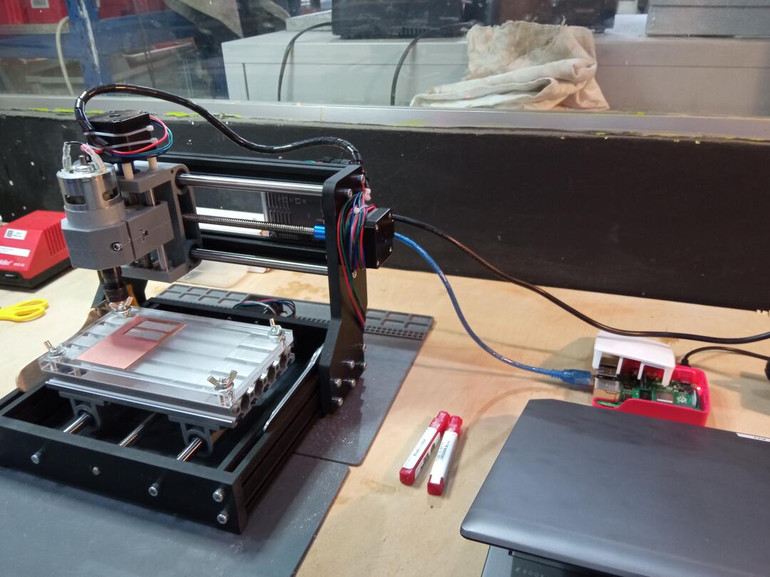
I just opened the case as you can see below to avoid overheating because there
an halogen lamp on the top heating the whole set-up.
Actual Milling
As I was convinced by the group assingment that the Conventional method was the neatest, I used this one on the desktop machine. But as you can see, the result is not so nice.
- Traces are torn appart
- Traces are missing
- Traces are too thin
Milling in Conventional mode
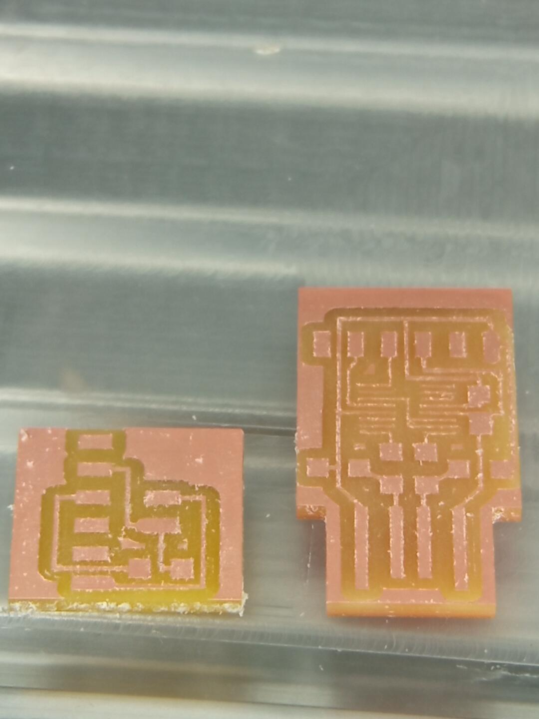
I started a new board but with the climb rotation which, looking back at the
group assignment seems to give wider traces despite its rough aspect.
The two finished board can be seen below. All the tracks are present and
are wide enough. The ascpet is not so nice but I checked that no short-circuit
can be provoked by the small imprecision.
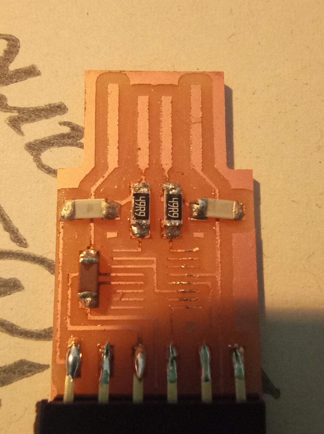
Stuffing
It was not my first time soldering, but with such small components it was indeed a first.
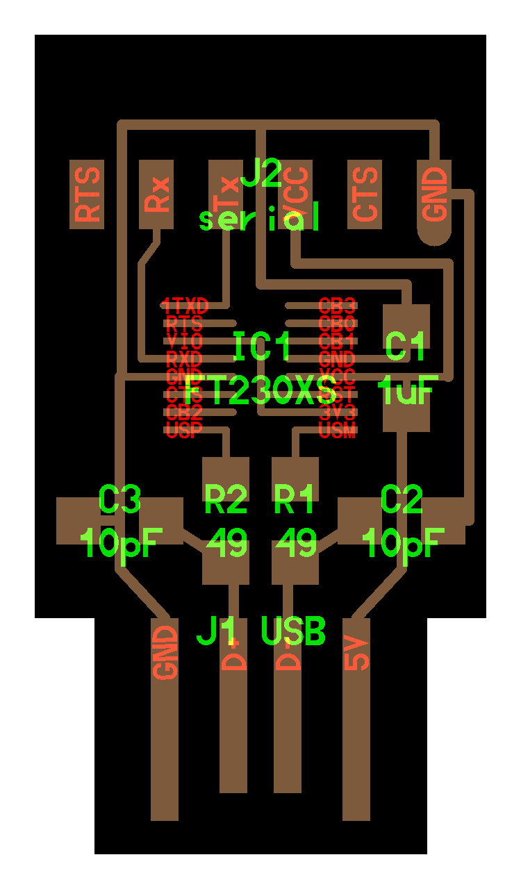
The components used are the following
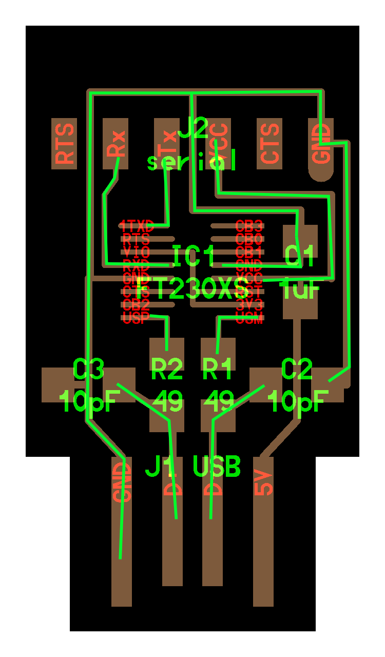
| Component | Description or type |
|---|---|
| C1 | 1uf |
| C2 | 10pF |
| C3 | 10pF |
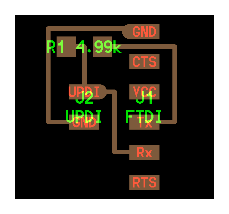
| R1 | 49 Ohm |
| R2 | 49 Ohm |
| J2 | serial |
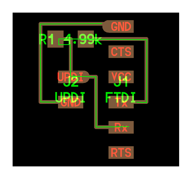
| Component | Description or type |
|---|---|
| R1 | 4.99kOhm |
| J1 | serial- 6 pin |
| J2 | 2 pin |
There is no surprise for soldering resistors and capacitors but the microchip was a tricky one. To sold it I used the following method :
- Apply tin on the traces only (without the MC)
- Place the MC on the tin-plated trackes
- Heat up the opposites legs of the MC with the iron and they will get fixed
It worked pretty well this way. But I strongly recommand to use a thin tin wire. I worked with 1mm and 0.2mm and the difference is huge.
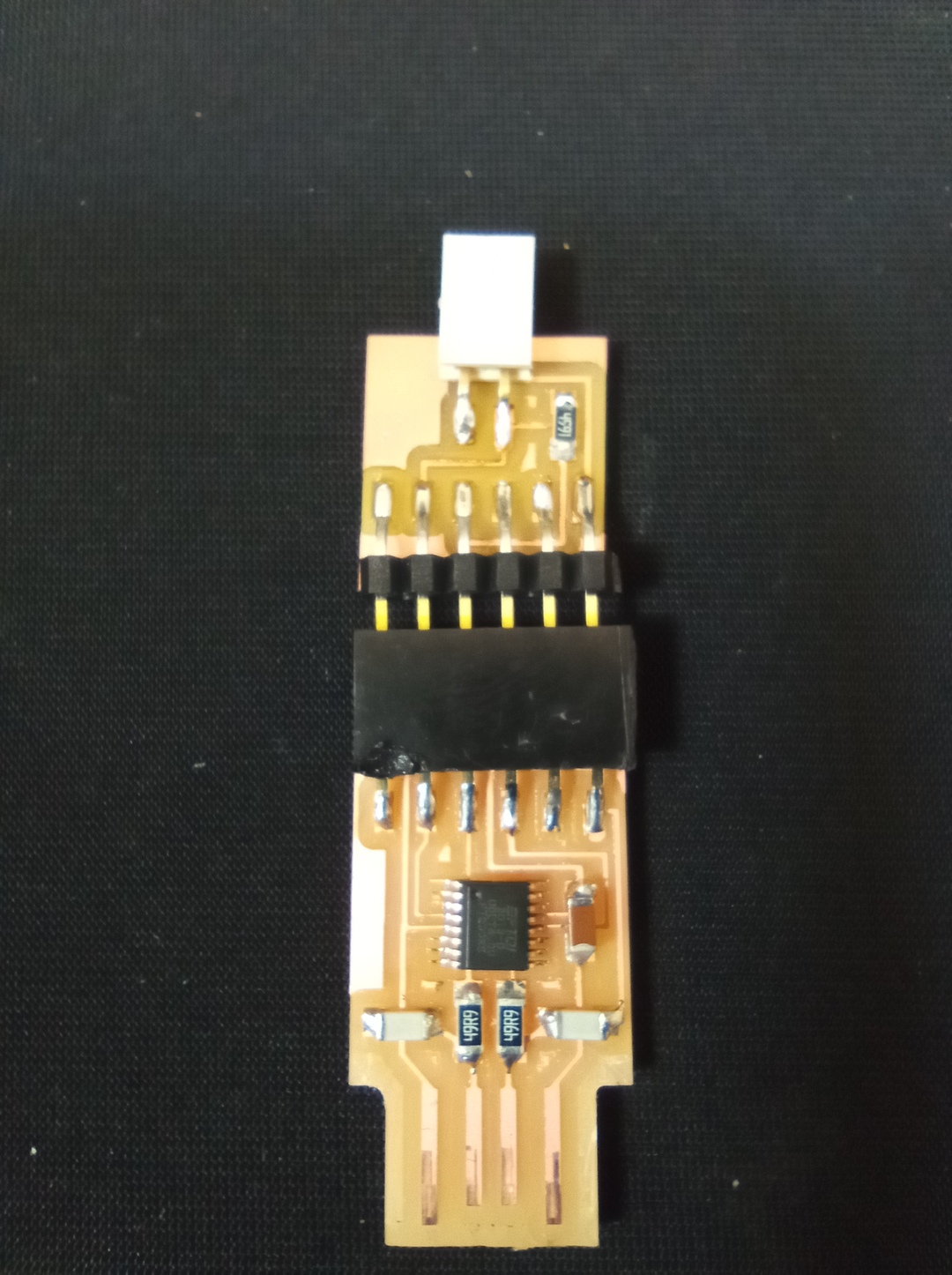
Here is the final result of my first board. Well the result was not so good.
I had to make a bridge on the upper-left leg due to a track that I ripped off.
It was fun to do, and working fine (conducivity validated) but not so
industrial compliant. Also the leg connected to +5V had no condictivy, and when
I tried to correct the issue I moved the whole micro-chip.
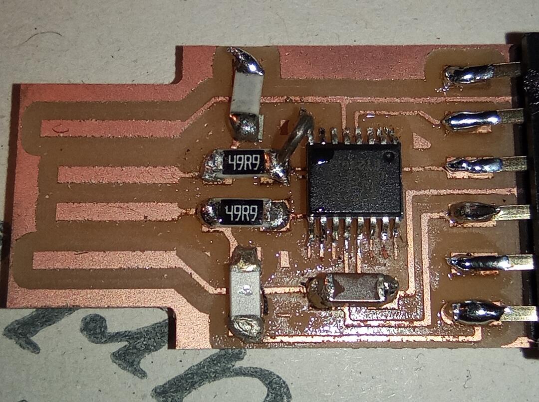
Based on my previous experience I milled/stuffed a new board and the result
was much better, I had it done in 30mn !
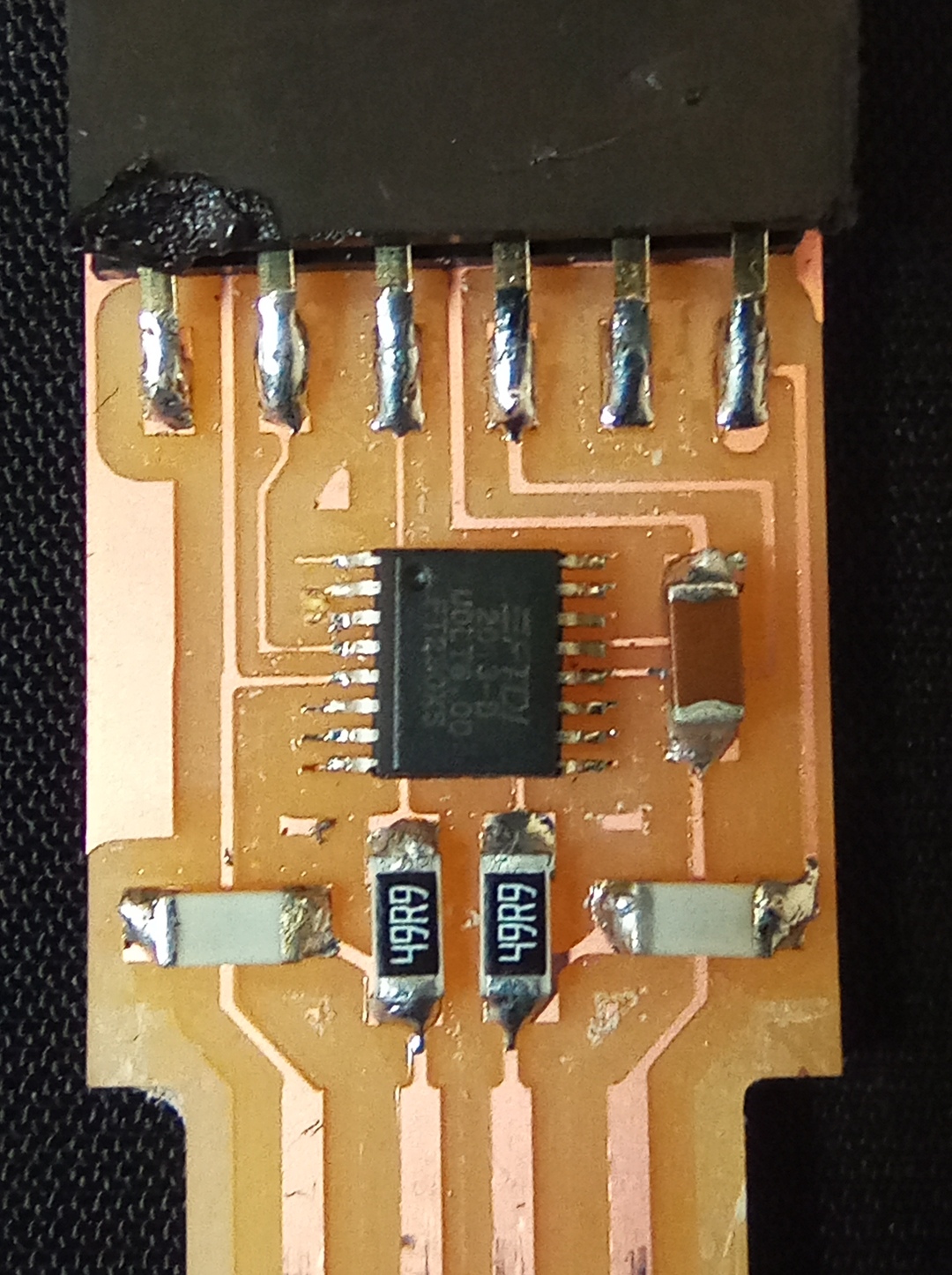
I have not mentionned the FTDI-UPDI board up to now, but I had no issue with
this one and it worked fine on the first trial. The only important thing to
mention is that I chose to do 2 separate board to save time. And I did well
because as I had to repeat the USB-FTDI it was less work.
Testing
Conductivity
The soldering looks nice, but before pluging it into my brandnew Raspberry,
I tested the tracks as you can see below –> no red line  .
.
Testing on the Pi
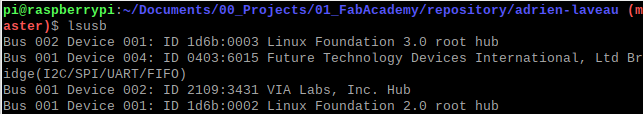
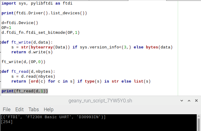
The lsusb command allows us to see what is plugged in the usb ports. The
information ‘bus 001 device 004 : ID 0403:6015 Future Technology Device International’
allows us to confirm that the board is correclty detected.
Going further
$ sudo apt-get install libftdi-dev
$ sudo pip3 install pylibftdi
Files
Boards
- Group assignment traces
- Serial - UPDI : Interior
- Serial - UPDI : Interior nc file
- Serial - UPDI : Design
- Serial - UPDI : Traces
- Serial - UPDI : Traces Climb
- USB - FTDI : Interior
- USB - FTDI : Interior Nc file
- USB - FTDI : Design
- USB - FTDI : Traces
- USB - FTDI : Traces nc files Climb
- USB - FTDI : Traces nc files Conventional
Python interface experiment
Lectures note
Introduction
Microcontroller
Put info below in a table
Microcontroller vs MicroProcessor MC : 5v or 3.3v even 1.8v (good for energy consumption) can interact with other units –> main point Program memory stays Pins are all the pins Ports are the ones that communicate with outer world
Registers is the state of the pins at a specific clock cycle
Tip
MP : 5 or 12V can compute and do complexe operations
How to choose your microcontroller - use a well known chip (ex : Arduino one) - depends on your electronic level - check on github how projects are used MC with wifi/bluetooth is ESP32. This chip is used in feather ESP32 from adafruit (check founder from Limor fry) ESP is the manufacturer, the number is the fucntion (espressif company)
Micrcontroller are not open ! RISC-V they want to do the whole hardware open.
FabModules - Input PNG file > 1000dpi & black & white - tool is only on the black part ! so we have to invert the image - give instruction (diameter, speed) - click “calculate” - shows the path
Objective -> FTDI chip detected Use USB extension to test first, not to destroy the computer
We are gonna program with UPDI. It has two standards 1. normal connector with lots of pins (FTDI) 2. adatper with the resistance between TX and RX (UPDI) Good to make the two boards.
Better to make small board to make them fast. So for me better to make several boards 1/64 tool for interior 1/34 tool to cut the board
When cutting if two traces the fisrt cut, the second one cleans.
Assessment
Group assignment:
Characterize the design rules for your PCB production process
Individual assignment:
Make an in-circuit programmer by milling and stuffing the PCB,test it, then optionally try other PCB processes.
Learning outcomes
Described the process of milling, stuffing, de-bugging and programming Demonstrate correct workflows and identify areas for improvement if required
Have you?
Linked to the group assignment page Documented how you made (mill, stuff, solder) the board Documented that your board is functional Explained any problems and how you fixed them Included a ‘hero shot’ of your board