6. Electronic Design
Group assignment
This year objective for the Fabacademy code club in Barcelona is to develop a solar powered website. More info here at The resurrected web.
During this project we had an issue with the MPPT (maximum power point tracking) board which stopeed outputing the 5V we needed to run the Pi zero. So we decided to use the investigation as a group assignment.
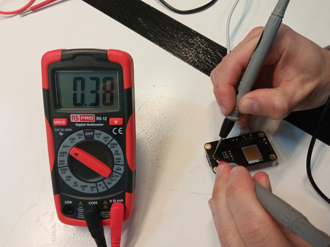
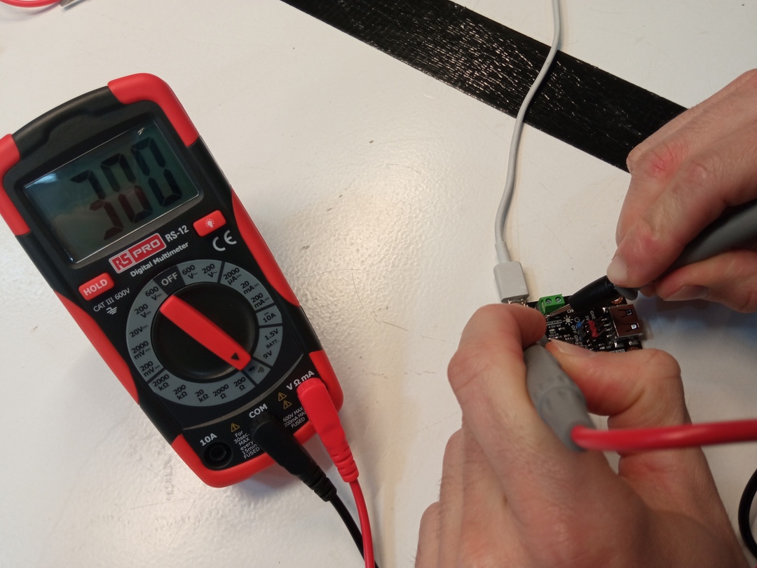
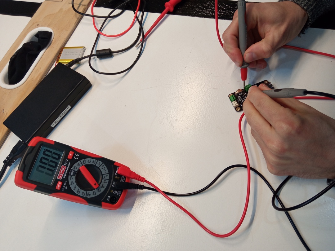
On the picture below you can see the measurment on the USB out pins where the voltage drops from 0.83V to 0.xxx volts in a few seconds. It looks like a capacitor discharging slowly.
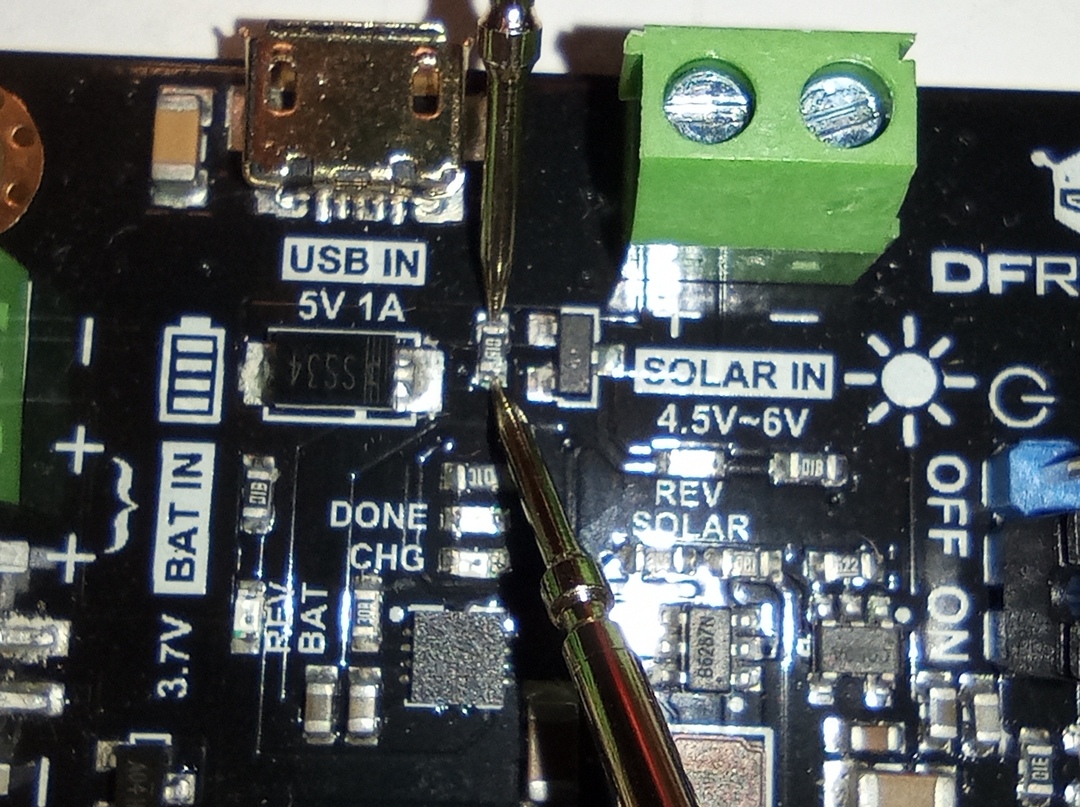
The board inputs are the solar panel and battery power. It will regulate the energy input in function of the battery State of Charge, Solar Panel Power and USB output.
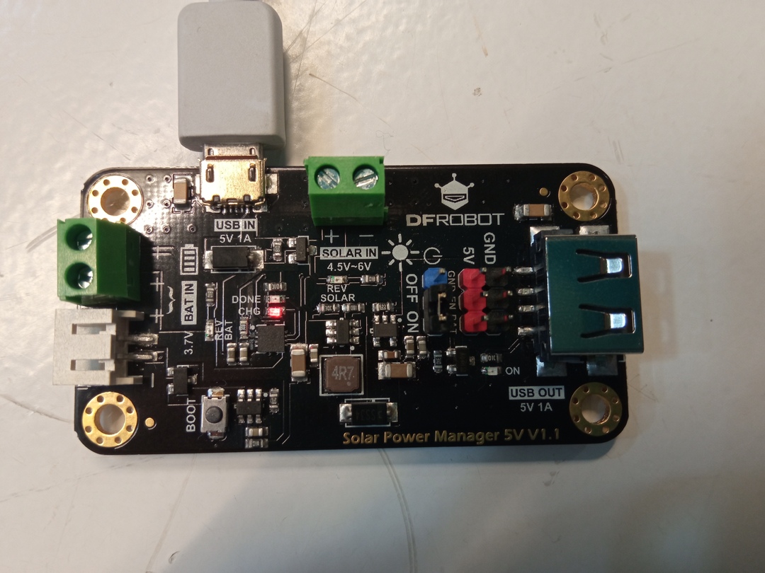
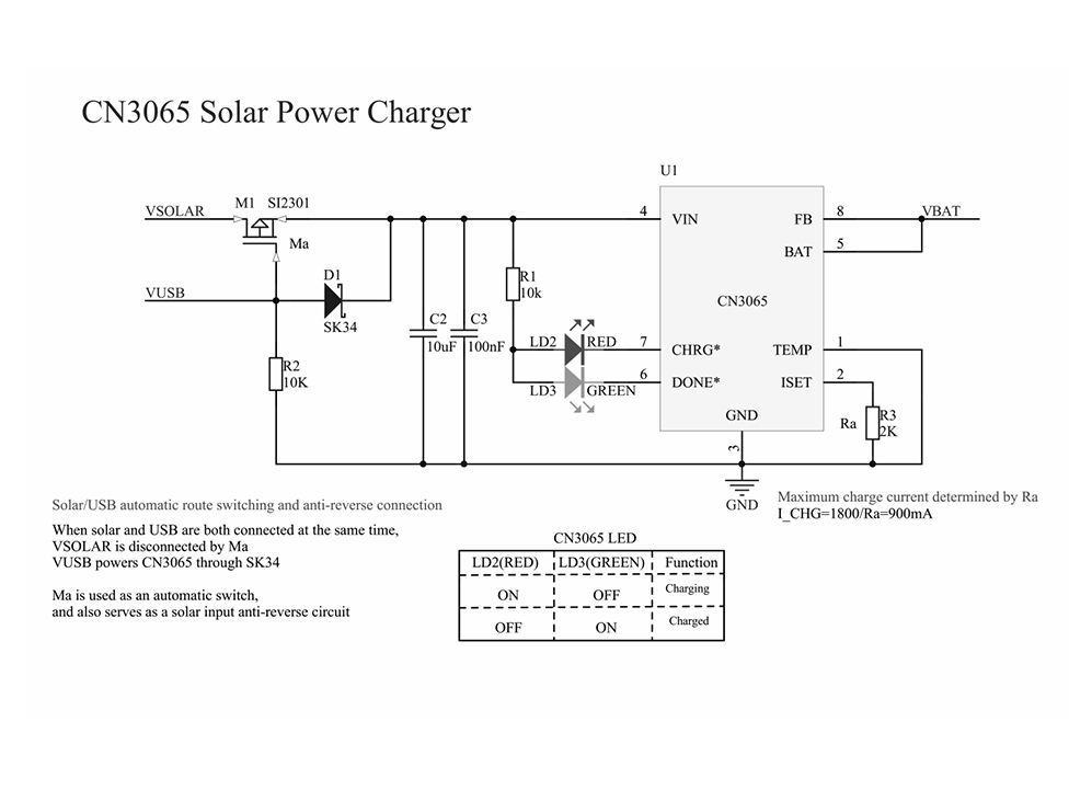
As the USB output voltage was not working as expected we based our study on the following diagram.
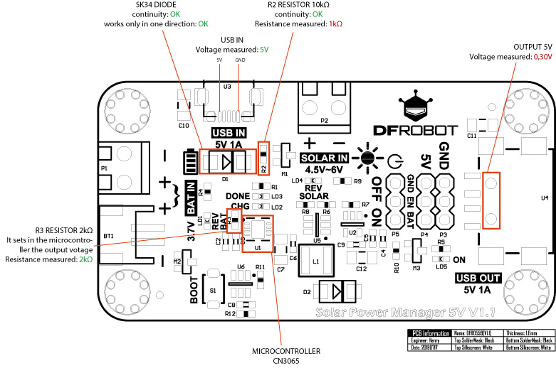
We started our analysis with the following scheme from the board datasheet.
Voltage inputs
The diode D1 is fine, the multimeter on “diode mode” is beeping in one direction and not the other one.
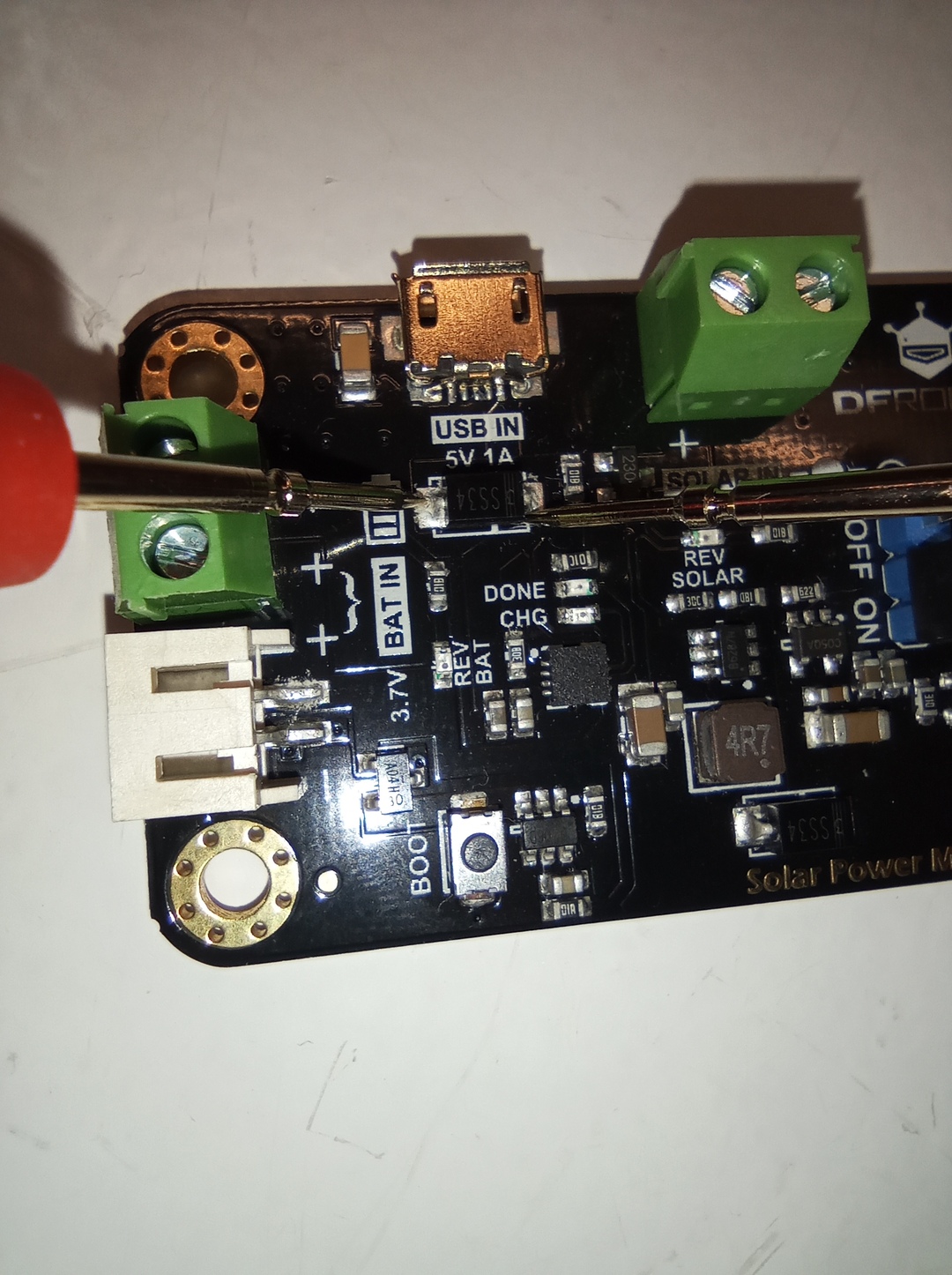
The resistance is also fine .
LIPO IC
The we started to think the LIPO regulator was not working fine because the heatsink was really hot and it smelt bad.
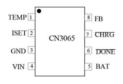
We used the datasheet of the CN3065 IC to know which pins to check.
We also check the R3 resistance.
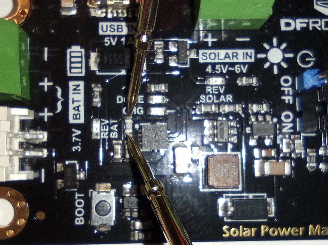
Finally our investigation lead to the measurement of the output voltage of the IC CN3035 (pin 8 and 5) which was giving less than 1 volt when it should have been charging the battery.
We concluded that the IC was burnt and had to stop the investigation here.
This testing was the occasion for us to use the measurement equipement we have in the lab, read datasheet, and make troubleshooting of a reasonably complicated board.
Personal Assignment
I will use this week to try and work with the potential microprocessor I will need
for the final project.
Here is my first draft of the functions, input, output and potential board
repartition I have in mind.
Choose the Micro Controller
What will I do with the MC ?
To prepare a board design we have to answer the following questions :
- How will I program my board ?
It will depend on my processor, I will answer later on.
-
How will I power my board ?
In my case the board will be placed in the fuse box of my house and it should have constant alimentation based on 220V available here and might use USB transformer (5V input).
-
What does my MC has to provide ?
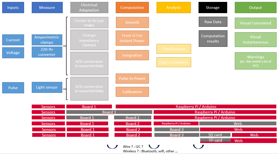
    1. Inputs**
        9 analogic inputs (8 Current + 1 voltage)
        1 birnary input (light pulse)
    2. Outputs
        1 binary for information (I2C ?)
        2 LED for information
    3. Resolution
        AVR has 8bit resolution.
            - Signal 220V
            - 8 bit = 256
            - Voltage Resolution = 220 / 256 = 0.8V
            - Current Resolution = 10A(max) / 256 = 0.039A = 39mA
    4. Wifi
    5. Maybe bluetooth
What options do I have ?
-
ESPRESSIF - ESP32-WROOM-32D : datasheet
- ADC : 15 pins
-
ATR - MEGA328P : datasheet
- ADC : 8 - 10-bit in TQFP and QFN/MLF package
-
ATMEL - TINY3216F : datasheet
- Freq : 20MHz
- pin : 20
- Flashable Memory : 32kb (10.000 cycles)
- EEPROM : 256 bytes (100.000 cycles)
- SRAM : 2kb
- ADC : 2 –> not enough
I will choose the ESPERSSIF ESP32 WROOM 32D board. To run it needs :
- 3.3V input voltage
- A reset button
- A slide switch for programmation
Design
The design of my helloboard for ESP32 is based on the Barduino design one can
find at https://gitlab.com/fablabbcn-projects/electronics/barduino.
I chose to work base on the Barduino FTDI 2.0 version as the programer I made
during the electronic production week is a USB-FTDI one.
I decided to respect the following rules for my design :
- Respect the original elements of the Barduino 2.0
- Keep the pin headers to reuse the board for embedeed programming week
- Make it such as a header for my sensors can be used
- Add a new switch + LED for the assignment
- Make it wide to ease the design (and still it’s complicated
 )
)
I realize that this board is a bit too much for this assignment but I will do it to see all the issues I might have with the chip in advance and to better prepare my final project.
Setting up Kicad
To set up Kicad the guide from FabLab Barcelona is pretty useful. It can be found in the local documentation.
Downloading
To set up the libraries of components, as I am working between my personal computer (Windows) and my raspberry (Linux) I use two methods to update them.
Windows
I download the libraries directly in ZIP format from the following repos :
FabLab Symbol & Footprints : https://gitlab.fabcloud.org/pub/libraries/electronics/kicad
Official Kicad Symbols : https://github.com/KiCad/kicad-symbols
Official Kicad Footprints : https://github.com/KiCad/kicad-footprints
Linux
First use :
- FabLab Symbol & Footprints : ‘git@gitlab.fabcloud.org:pub/libraries/electronics/kicad.git’
- Official Kicad Symbols : ‘git clone git@github.com:KiCad/kicad-symbols.git’
- Official Kicad Footprints : ‘git clone git@github.com:KiCad/kicad-footprints.git’
After :
git pull //from each folder
Linking
Once the repo are uptodate you can link the repo to kicad from the main window using the menu ‘Preferences => Manage Symbol Library and Preferences => Manage Footprint libraries’. In the ‘Configure path’ one can add the variable FAB that points to the FabLab Kicab library to have the 3D models availabe in the desgin.
Schematic
The schematic was done on Kicad as follows.
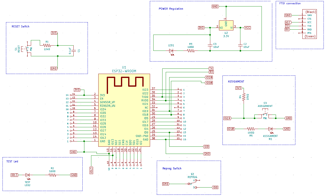
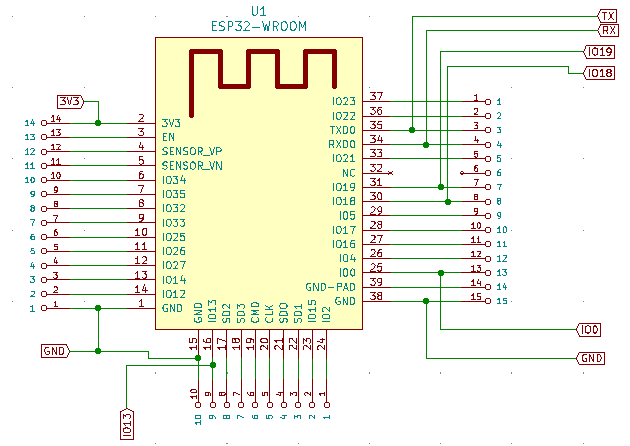
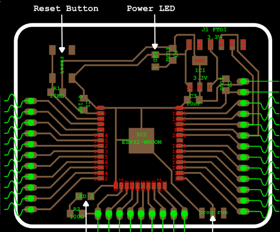
The ESP32-WROOD-32D from Espressif is the core of my board. I chose it for its high number of ADC (Analog Digital Converter) and its integrated wifi function. Its datasheet is available here and a more detailed version here. The pins that are used are :
- 3V3 : voltage pin for powering the chip
- TX/RX for communication
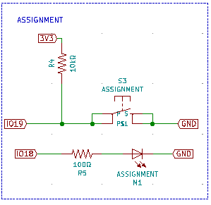
- IO18 / 19 for the assignment (button and led)
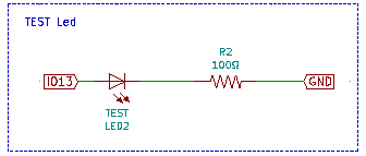
- IO13 : Test led of the original Barduino design
- IO0 : for letting the board know we want to program it.
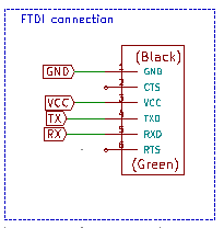
The FTDI Header will allow us to connect the programer to the board and power it. We use VCC, GND and TX/RX pins.
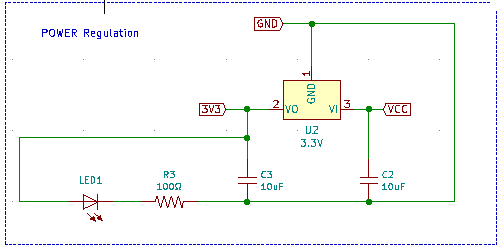
Power regulation has to be done as the ESP32 works at 3,3V and the USB will provide 5V. It comes with the 3,3V regulator components and 2 capacitors to filter the voltages; 10uF is a common value for this kind on set-up. The LED+Resistor is here to confirm presence of power. To find the correct Resistance for the led we do the following calculation based on the Green LED datasheet :
- base voltage : 3.3V
- LED voltage drop : 2.1
- LED testing current : 10mA
- Resistance = U/I = (3.3-2.1)/0.01 = 120 Ohm
Danger
The 3.3 and 5V regulator looks alike and can be easily mixed up.
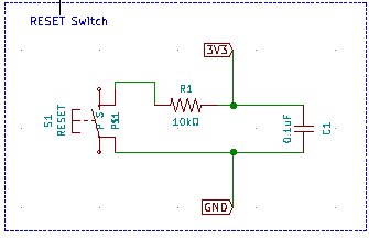
I will have to study this part during the embedded programming week, but it seems that the ESP32 knows that we want to flash it when the pin IO0 is set to ground. The slide switch is here for that purpose.
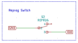
This switch is a reset switch but I do not fully know its purpose at the moment.
The Barduino team set up a testing LED as we do for the assignment.
The assignment of this week consist in adding a LED that lights-on based on the input of a push-button. The push button comes with a pull-up resistor to avoid ambiguous state of the pin IO19.
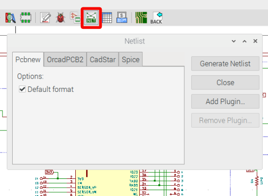
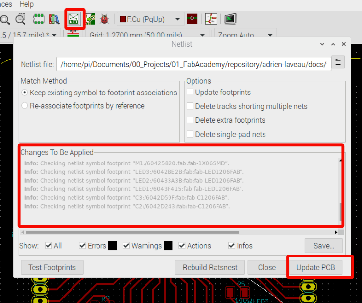
Create a NETLIST Before ending the schematic part, when the design is ready, one has to crate a netfile which will transmit the information needed to the PCB module to place the components.
No big secret here, we have to click on the small NET button as shown below and keep the netfile in a safe place.
Bill of components
| Reference | Value | name |
|---|---|---|
| U1 | ESP32-WROOM | ESP-WROOM-32U |
| U2 | V regulator | LDO 3.3V 100mA |
| R1 | 10 k Ohm | Thermistor NTC 10kOhm |
| R2 | 100 Ohm | RES 100 Ohm |
| R3 | 100 Ohm | RES 100 Ohm |
| R4 | 10 k Ohm | Thermistor NTC 10kOhm |
| R5 | 100 Ohm | RES 100 Ohm |
| C1 | 0.1uF | CAP CER .1uF 250V |
| C2 | 10uF | CAP CER 10UF 50V |
| C3 | 10uF | CAP CER 10UF 50V |
| LED1 | LED GREEN CLEAR | |
| LED2 | LED GREEN CLEAR | |
| LED3 | LED RED CLEAR | –> GREEN |
| S1 | Button switch | |
| S2 | Slide switch | |
| S3 | Button switch | |
| M1 | FTDI Pin Header SMD | CON HEADER SMD |
FootPrints
Now that the design is ready, we have to go through the following procees
to create a correct footprint to be produced.
1. Define our design rules
1. Place the components
1. Create the tracks
Design rules
In the PCB module one should go to File -> Board Setup and set the Design rules as follows if using a Roland Milling machine like we have in our FabLab.
The Design rules were chosen based on the group assignment test done during the electronic production week which lead us to see that the minimum track width should be around 0.4mm.
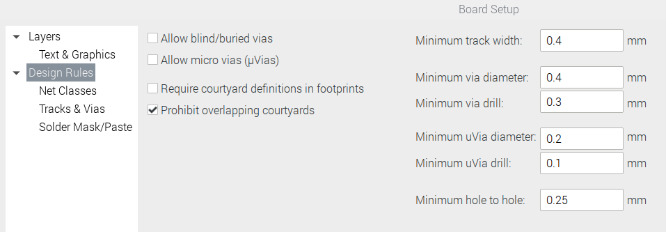
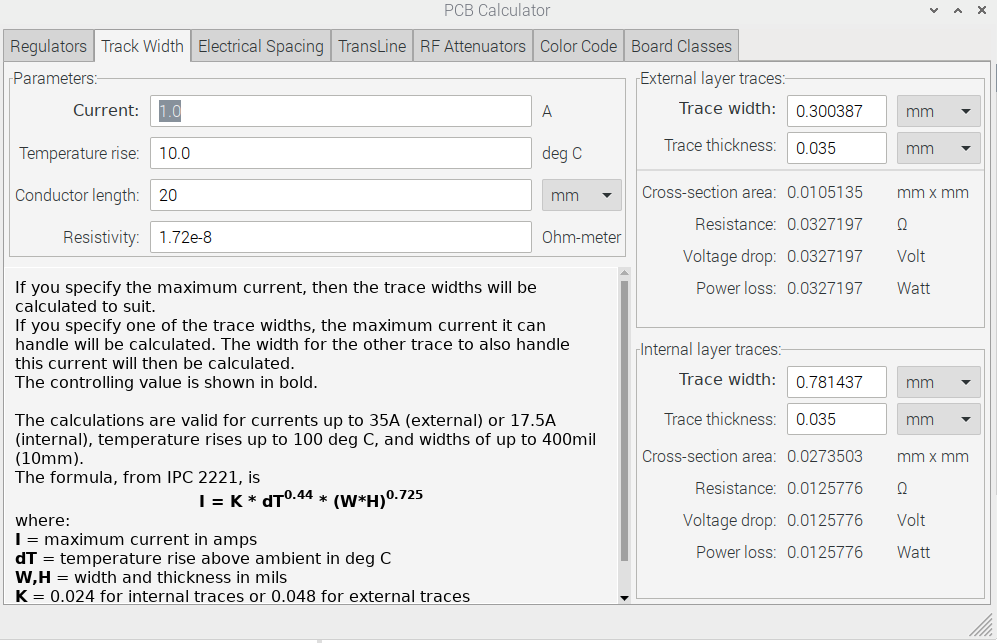
To confirm the value with respect to the design one can use the Calculator module of Kicad which will take into account the board usage to provide track width recommandation based of heat echange prpoperty of the board.
Setting up the PCB
-
Netlist
When switchting to the PCB module the first thing to do is to load the NET file created at the end of the schematic module. It will load the components indicated in the schematic and the relation between their pins to help the user to route the different tracks. Click on the button show in the image below to load it. Confirm that there is no error and then click on the Update PCB button.
-
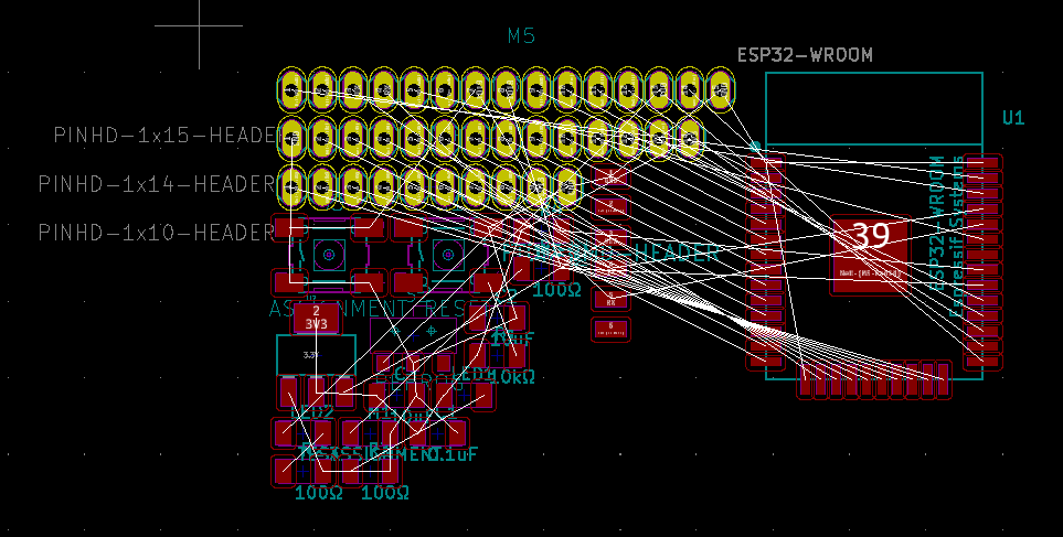
Placing the components
After loading the netlist; all the components are placed randomly and one has to organize them. I learned from that step that placing the components has to be done thinking in the following points :
- Will the routing be feasible ?
- How will be my user interfaces : buttons, switch, jumpers etc…
- Where will my board go : casing etc …
- Use the occasion to double check the design (does it make sense ?)
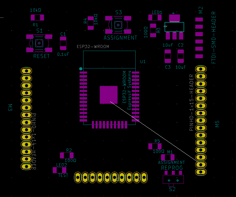
After a bit a thinking and inspiration from the barduino I got the solution presented below.
-
Creating the tracks
Now that the components are placed, on has to places the tracks thinking in the following points :
- Can I mill it ?
- Is the board “readable for debugging” ?
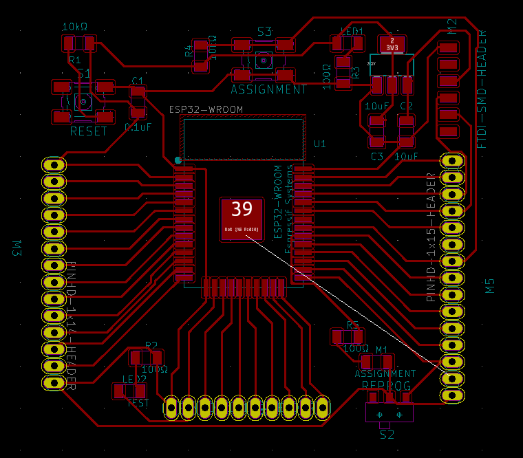
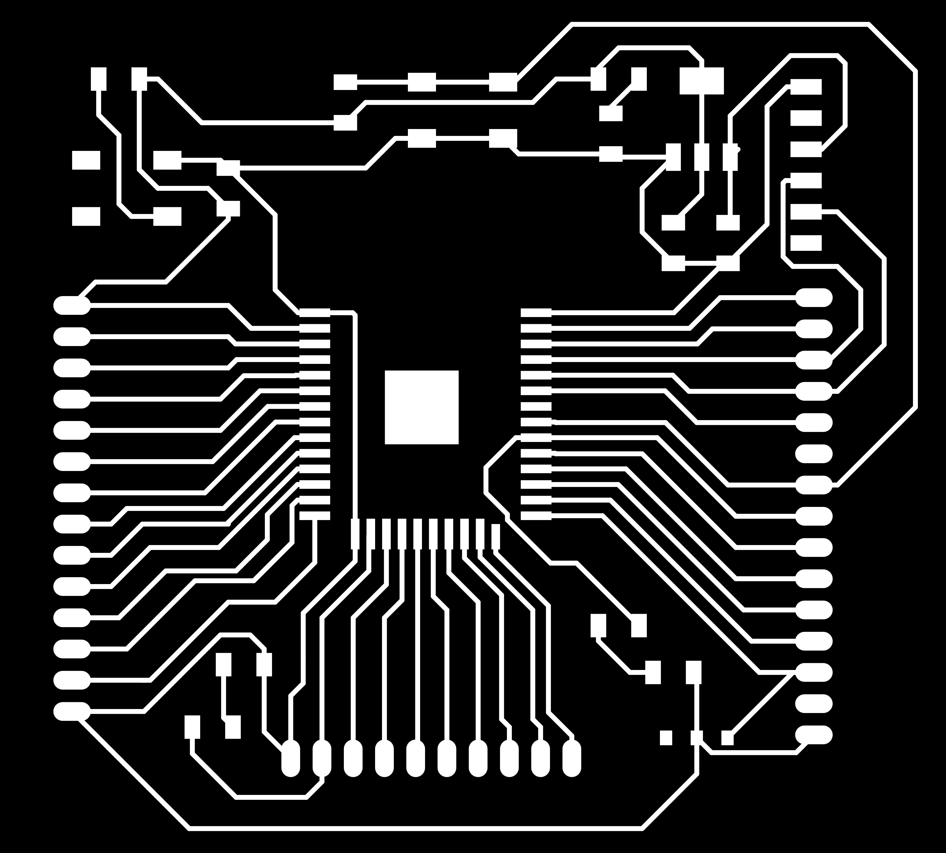
Here is my final routing :
-
The board Last but not least, one can create the desired shape of the board using the graphic line tool in the Edge cut layer.
-
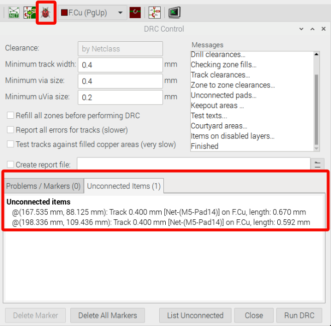
Board validation One last step before exporting our design is to use the Design rule check to confirm that the board respect our desgin rules. It is not a guarranty of succes, but no having it check is a garranty of failure
 .
.In my case I have an unconnected pin but it is said in the datazsheet of ESP32 not to connect it so everything is fine.
-
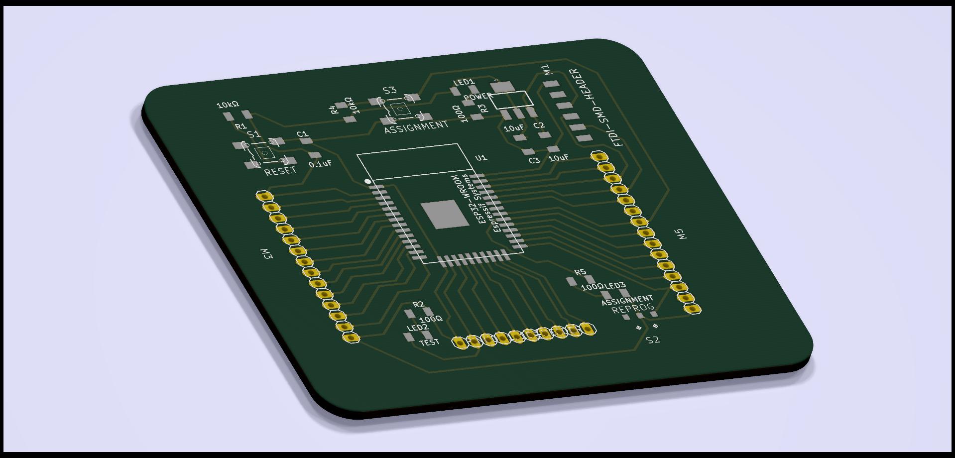
Final Result Just for fun, here is the 3D view of the final board. For more complicated design if one has the 3D footprint of their components it can be interesting to check in the 3D model that everything can be mounted and that there is no interface issue.
Export
Once the SVG has been exported from Kicad, we have two methods
Manual PNG creation
- Open inkscape
- Import the SVG file : File -> Import
- I use the default options of the import window (inkscape_import_svg_options)
- Create the layers
- Layers -> layers : open the layer menu on the side
- Create the following layers (+ button) : cut,traces,holes
- We add the elements to each layers
- Cut : click on the border once, and click again to select it -> right-click “Move to the layer” -> select “cut” in the window that appears.
- Hide the layer with the small
 to check that the desired part is in the layer
 - Repeat the operation with the traces and pads -> to layer “traces”
- Repeat the operation with the holes -> to layer “holes”
- To fill a layers with color using the “Paint bucket” (for next step)
- Select the layer
- Click on the paint bucket
- Select the desired color
- Click in an empty area of your layer
- Now we have to set the correct colors
- traces must be white (no action from the milling machine)
- Fill the empty area with white (at the moment it is transparent)
- Extensions -> Color -> Negativo
- Holes must be black to cut them
- Cut must be white inside and black outside
- To do so
- Select one layer
- Select its content
- Extensions -> Color -> Negativo
- traces must be white (no action from the milling machine)
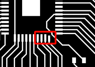
I used inkscape to reduce the size of the pad because it was easier done than on freecad. In the red square the right pad is a bit shorter than the other pads.
Automated procedure
I did not have time to test it but all the info is [here](https://gitlab.com/fablabbcn-projects/electronics/kicad-exports).
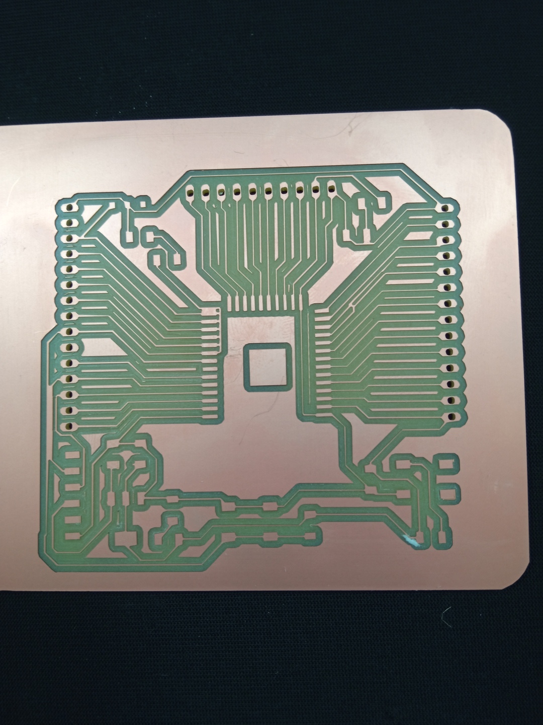
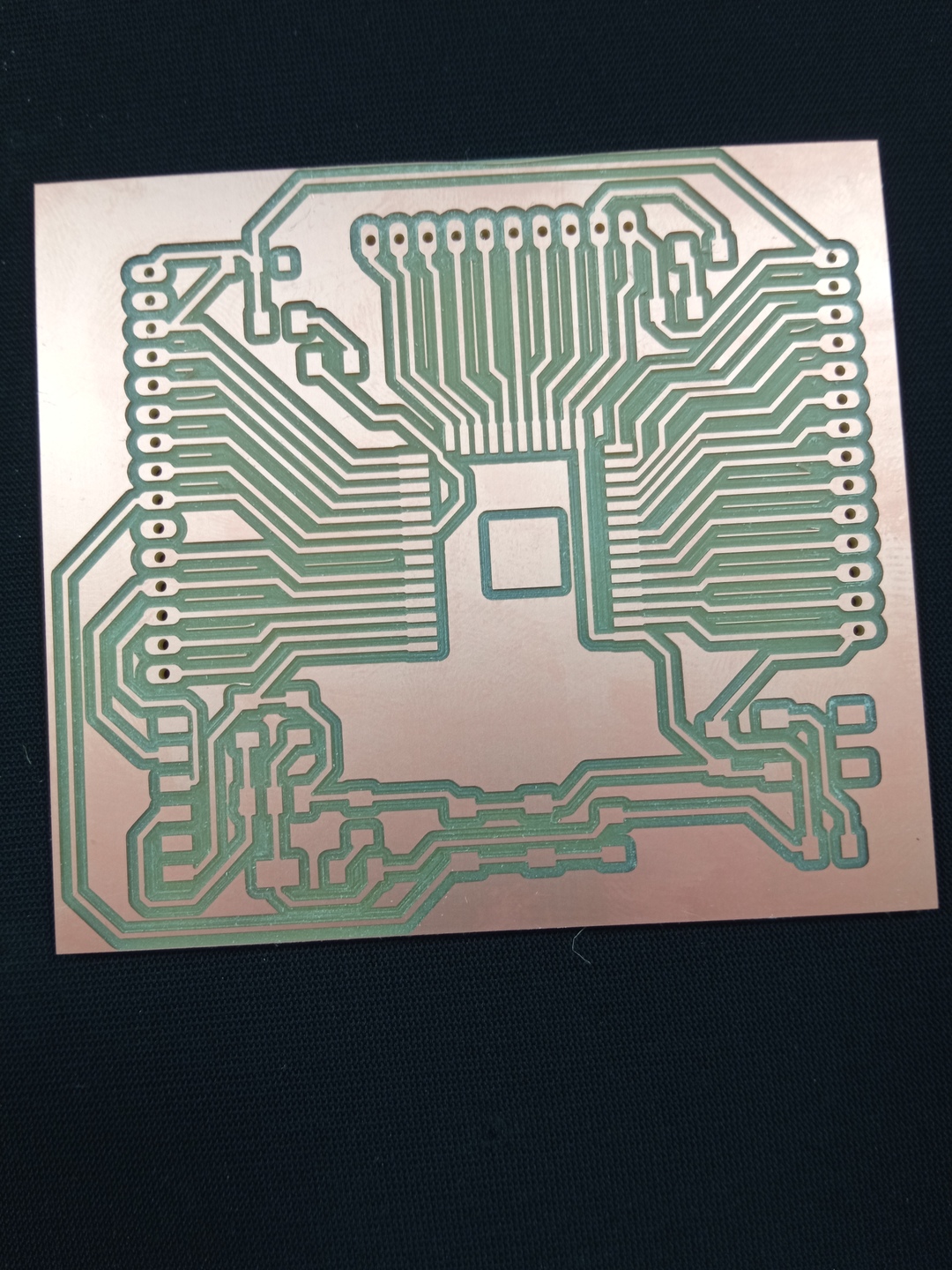
Production
- Preparing the files for Roland
- Select the PNG file
- Select the “mil traces” with the 1/64 tool
- Cutting in Climb
- Cutting Speed : 3mm/s
- Origine : 0,0,0
- Jog height : 6mm
- home : 0,0,20
They have to be milled before the outline
- Select the PNG file
- The holes have to be black (to be removed). If need click on invert.
- Select mil outline
- Select a cutting speed of 1.5mm/s max
- origine and home parameters as for traces
This is the last step
- Select the PNG file
- Settings are the same than for the holes

Testing
Now is time for testing the board
Power
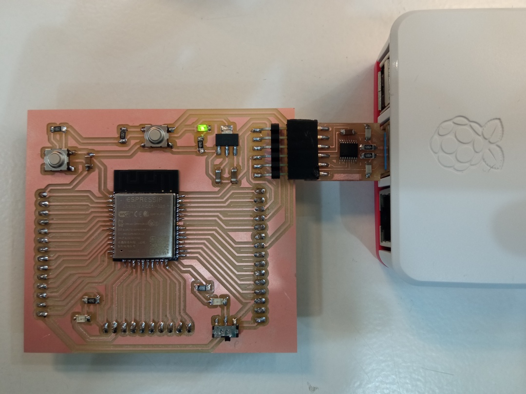
I plug it on the Pi and the power led works.
Troubleshooting the board
As explained in the next section I flashed a little blink program to my ESP board. But it did not worked directly because I made some mistake in the design.
-
Wrong wiring of the reset button
I did not read correclty the pin layout of the original Barduino and the Reset button was not wired as it should.
- Desired effect : Pin “EN” has a pull up resistor. And when pressing the button it is set to ground. Otherwise the pullup resistor keep it to high logic level.
- Error effect : Pressing the button short the 3.3v and the ground through a 10kOhm resitor and the reset does not work.
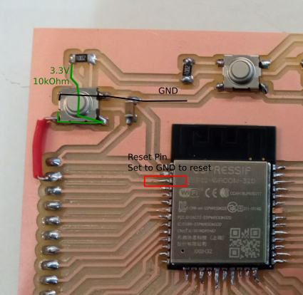
Note
The barduino Pin layout comes from the official barduino website : https://gitlab.com/fablabbcn-projects/electronics/barduino/-/raw/master/img/Barduino2.0-Pinout.png
-
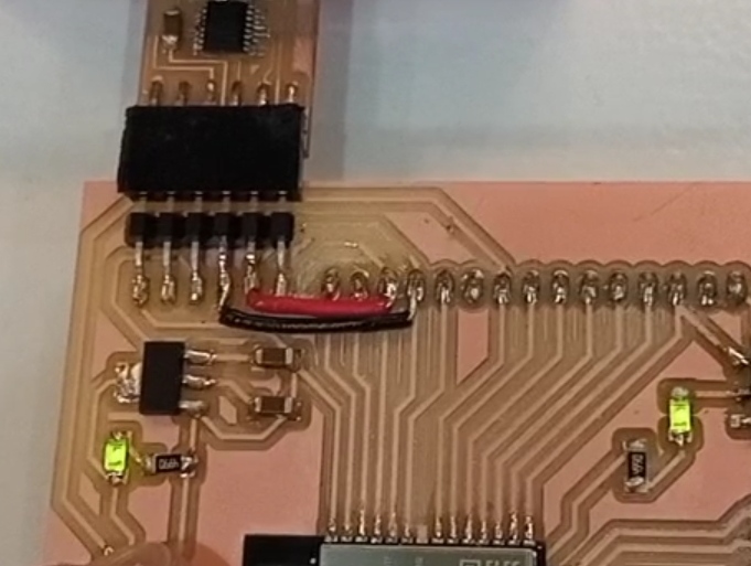
TX/RX wiring
Once the reset button was repaired, the flash was still not working. When routing my path in Kicad I though I was making the correct thing of paring TX of the Pin header to the TX of the ESP and same for the RX. But it was an error, TX has to be linked with RX and RX with TX. To correct this I had to remove the TX and RX tracks and solder two wires.
Blink a led
Thanks to the final reparation of the board (reset button and TX/RX rerouting) I was able to flash my board.
The complete section is transferred here : Embedded programming week 8.
Files
-
Full kicad project. The useful files are the following ones
- Kicad project : helloboard_ESP32WROOM32D.pro
- Kicad Schematic : helloboard_ESP32WROOM32D.sch
- Kicad PCB : helloboard_ESP32WROOM32D.kicad_pcb
- SVG export for Inkscape :helloboard_ESP32WROOM32D-brd.svg
-
PNG : for creating RML files edited with inkscape
-
RML : Files to be exported to Roland milling machine
Lecture Notes
Assessement
Learning outcomes
Select and use software for circuit board design Demonstrate workflows used in circuit board design
Have you?
Linked to the group assignment page Documented what you have learned in electronics design Explained problems and how you fixed them, if you make a board and it doesn’t work; fix the board (with jumper wires etc) until it does work. Included original design files (Eagle, KiCad, - whatever) Included a ‘hero shot’ of your board Loaded a program and tested if your board works