5. Electronics production
Learning outcomes
- Described the process of milling, stuffing, de-bugging and programming
- Demonstrate correct workflows and identify areas for improvement if required
Have you?
- linked to the group assignment page
- Documented how you made (mill, stuff, solder) the board
- Documented that your board is functional
- Explained any problems and how you fixed them
- Included a ‘hero shot’ of your board
Group assignment
For the group documentation, please check group assignment page here: Electronics production (Group page)
Individual assignment
For the individual assignment the objective was to make a in-circuit programmer. For reference used the Building the FabTinyISP.
FabTinyISP is a AVR ISP programmer/board that can be built by milling a PCB and removing the unwanted copper from the board. To do this it’s necessary to have a board design, with circuit tracks on it and component connection points, so that the CNC can then remove all the copper around the circuit tracks, keeping this way all the necessary connection for the circuit components to be electrically connected.
There are some steps to reach final board design for FabTinyISP.
- Make board schematic design
- Make board design
- Mill the PCB
- Board Stuffing/soldering
- Board testing
- Board programming
Board design
To make the board design i used EAGLE (Easily Applicable Graphical Layout Editor) a software that can design electronic schematics for printed circuit boards (note: This is something new to me so i’m experimenting and learning as i go). So in EAGLE you need to design the schematics of your circuit with all components connected. Once you have this, you can then create a board by using the PCB layout editor where you can route your components to create the PCB tracks or use the auto-routing feature :)
Note
I git clone the Libraries repository and then installed the fab.lbr into EAGLE. This allows to use the Fab academy components, most of the needed components are already inside this library.
To import a library into EAGLE, go to Library -> Open Library… and select the file from your repository: eagle/fab.lbr
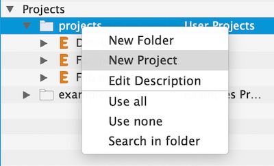
After opening EAGLE created the project by right clicking in the “projects” folder.
Circuit Schematic
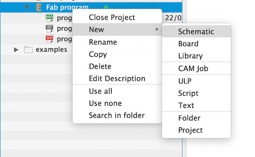
Created a new schematic by right clicking in the project name, to start designing the programmer circuit component connections.
To design the a circuit 1st need the component list:
| Quantity | Name | EAGLE reference |
|---|---|---|
| 1 | ATtiny45 | UC_ATTINY45SI |
| 2 | 1kΩ resistor | CONN_03X2_AVRISP |
| 2 | 499Ω resistor | R1206FAB |
| 2 | 49Ω resistor | R1206FAB |
| 2 | 3.3v zener diodes | DIODE_ZENERSOD123 |
| 1 | red LED | LEDFAB1206 |
| 1 | green LED | LEDFAB1206 |
| 1 | 100nF capacitor | CAP_UNPOLARIZED |
| 1 | 2x3 ISP pin header | CONN_03X2_AVRISP |
| 1 | jumper | SW_SOLDER_JUMPER |
| 3 | Vcc | |
| 5 | Ground | GND |
All of these can be found inside the “fab” library after clicking in the 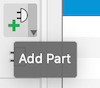 button.
From here is just a matter of adding componends into the schematic along with some VCC and GND components.
Following the schematic i added the components into EAGLE schema trying to have them in about the same place. Have also used the name 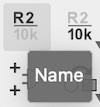 and value
 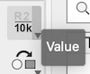 buttons to change the name of components and respective value (like for resistors). This the next step, making the connections, easier.
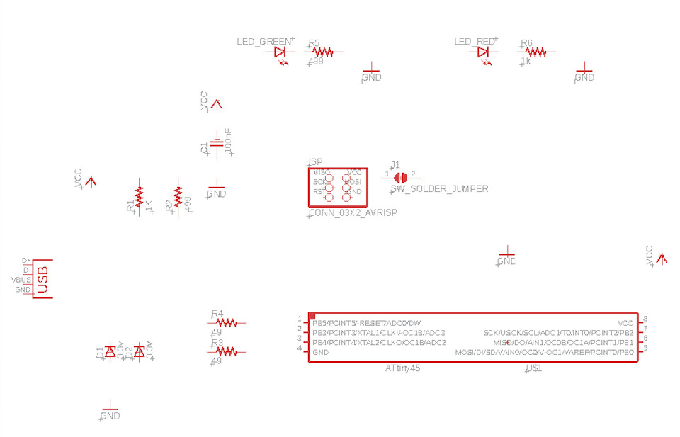
After placing components connections were made by using the Net  button

At this points we are ready for the next step, making the board.
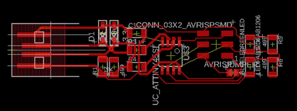
Circuit Board
From the the circuit schematic i clicked in the  button to open EAGLE board editor. This shows a empty board layout with all circuit components outside on the left bottom.
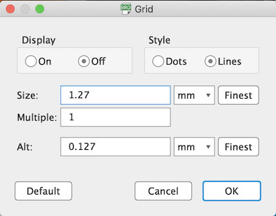
Changed the grid units to mm by clicking in 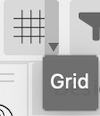
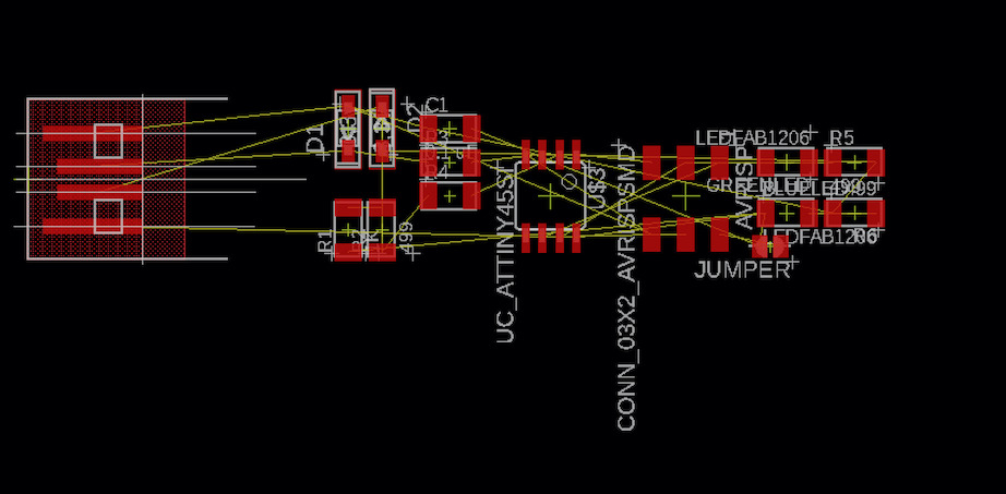
The task now was to move the components to the board, into place where the real board components will be soldered. This is done by clicking in the + of each component and moving them into the black square (the board), while moving you can also left click to rotate the component in a way that could benefit the connection with other components.
Tried to followed the placement from the FabTinyISP and organized the board as image below.
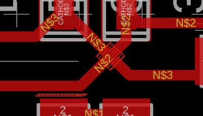
Now it’s time to route components. This will generate the circuit path between components that will be used to let copper in the board and allow the CNC to remove copper all around, to “print” the circuit in the board.
This step requires some iterations while drawing the routes with the  button. Why? because each route can’t cross over other, track distances, the final design needs to work on real world :)
After re-arranging components, making some routes i also tested the 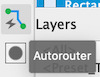 button. This makes EAGLE generate route between components in an automatic way. I choose to use “/” and only top board option.
Result? An almost ok board… almost because there are some highlighted red routes that are crossing or out of place. So this board will not work properly, but can always improve it by tweeking the component placement and routes.
EAGLE Tips
- Ripup button allows to remove 1 route at the time.
- “RIPUP ;” command will remove all routes from your board done previously via autorouter or manually.
- Ratsnet button to redesign routes in the shortest way after any component place change.
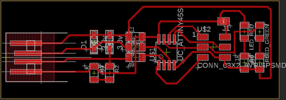
Decided to start v2 of my programmer and start from the beginning, reproducing all steps and after tweeking component placement and routes and reached a final board design that looks ok.
Board Making
Making a Copper tape circuit with the vinyl cutter
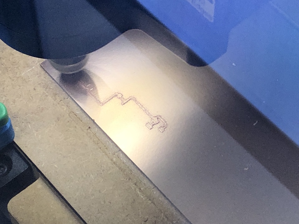
Exported the board from EAGLE in SVG file format and opened into Inkscape. In the end it required to generate bitmap from the vector drawing and work in inkscape with a PNG image because the traces on Inkscape didn’t have any width. So image was resized to match real mm size and cutted in the copper tape.
The Copper tape was glued on top of the vinyl to give it support during the cut. Did some tests before cutting the final circuit.
This is the final circuit in the copper tape.
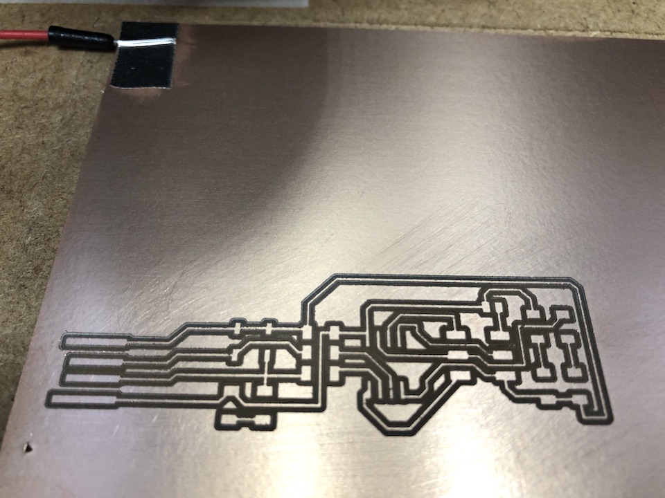
After the post-processing to remove the unwanted copper around the circuit with fine tweezers and a bit of patience. Final result in below image.
At this points i was ready to start stuffing and soldering components into the vinyl board circuit. It was a slow process because i was trying to keep tracks glued to vinyl, not make a hole in the vinyl with 300C soldering iron or break the copper tracks. Flux helped and managed to solder every component with success. Have tested every component solder in the circuit with a digital multimeter, to be sure all components were connected to tracks. Have soldered a usb cable into the usb connector tracks to later program the board.
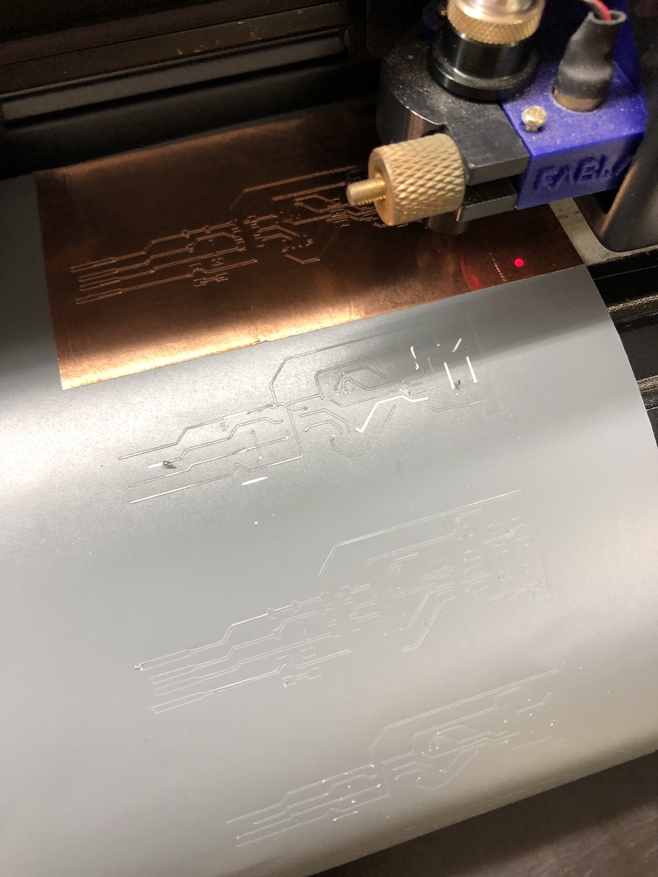
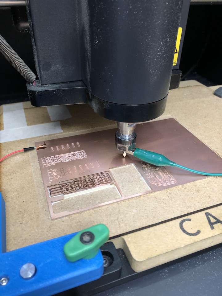
Making a PCB circuit using CNC
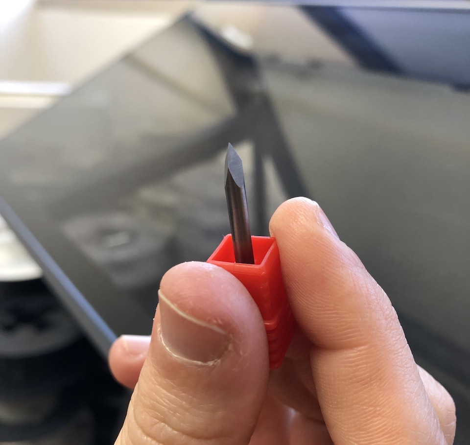
Have used same circuit design to make a PCB by using lab Carvey Desktop CNC.
The tool used to remove the copper from the board was a DIA 0.2 endmill.
For first step was connect and initialize the CNC. This was done via CNCjs (a web-based interface for CNC).
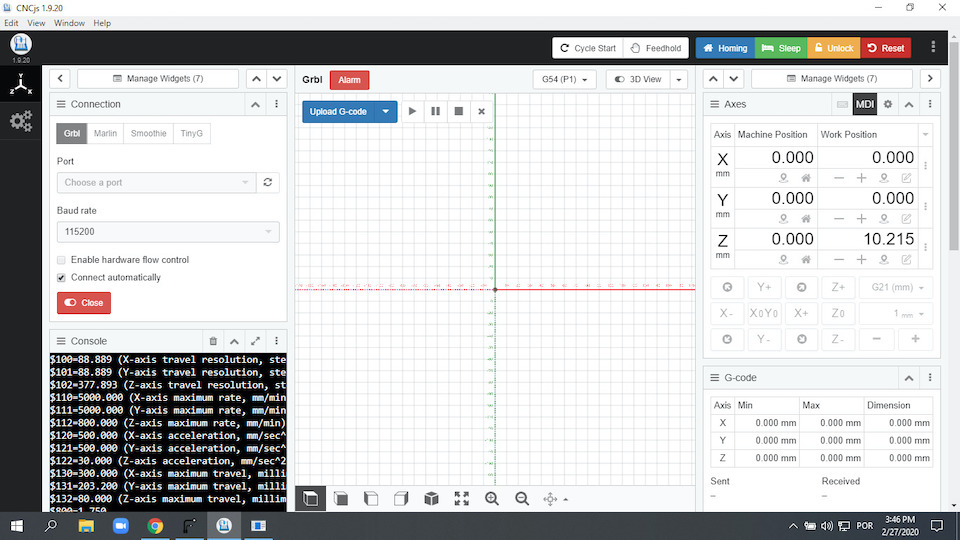
and zeroing the CNC.
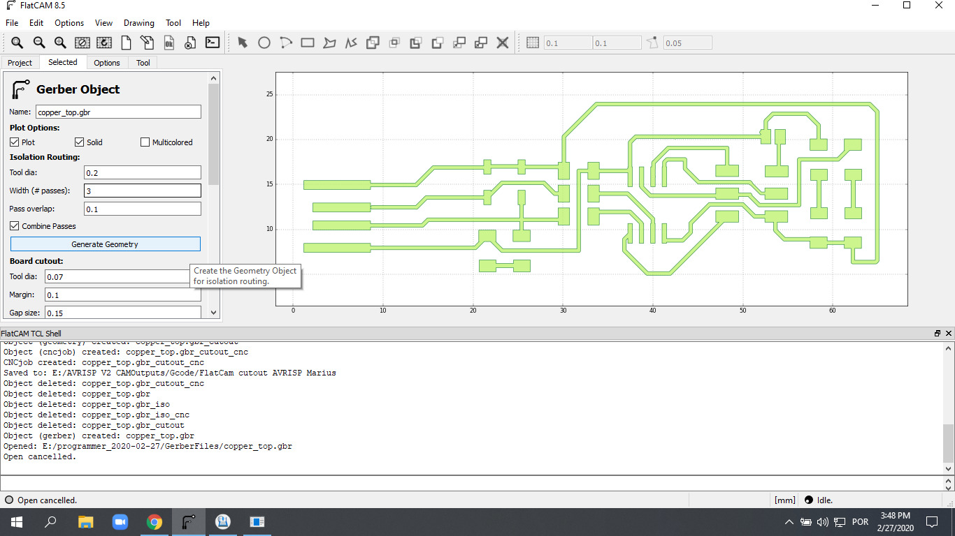
After exported the CAM data from EAGLE via  button. Then fetch the Gerber file “copper_top.gbr” from the EAGLE project sub-directory “CAMOutputs/GerberFiles” and moved into FlatCAM (Free and Open-source CAM software for PCB milling).
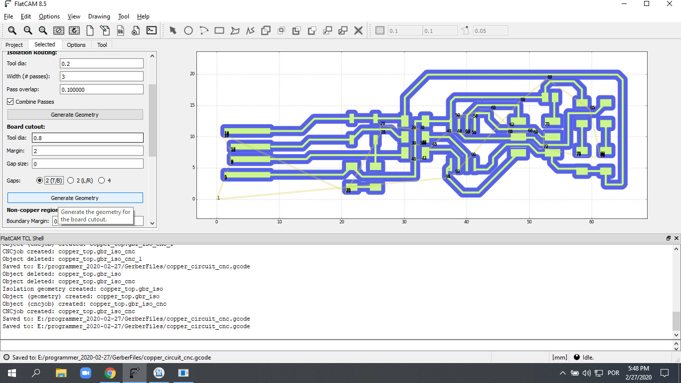
After opening the “copper_top.gbr” in FlatCAM started to set settings in “mm” for Gerber options:
- Isolation routing:
- Tool dia: 0.016
- Width: 1
- Pass overlap: 0.15
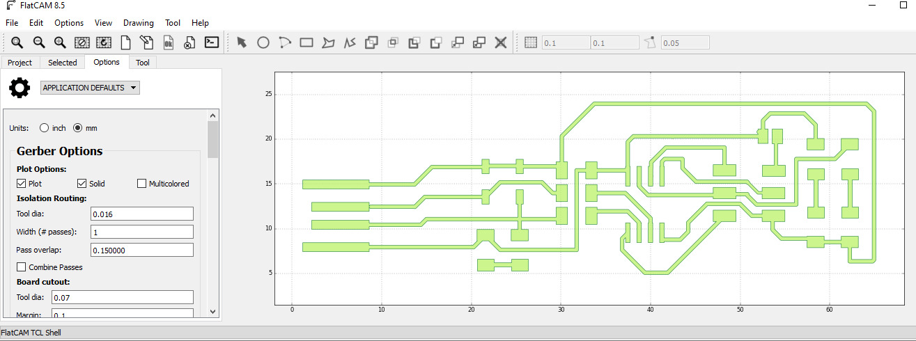
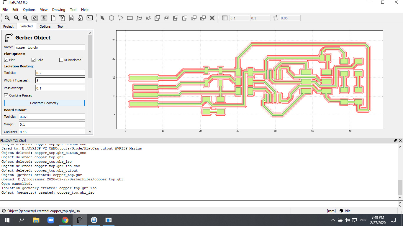
Then for the selected Gerber object:
- Isolation routing:
- Tool dia: 0.2
- Width: 3 (# of passes)
- Pass overlap: 0.1
- and with Combine Passes
And generated the isolation geometry for circuit
And as last step on FlatCAM generate the CNC job file to pass into the CNC. For this changed the following settings:
- Cut Z: -0.065
- Travel Z: 1
- Feed Rate: 100
- Tool dia: 0.2
- Spindle speed: 12000 (rpm)
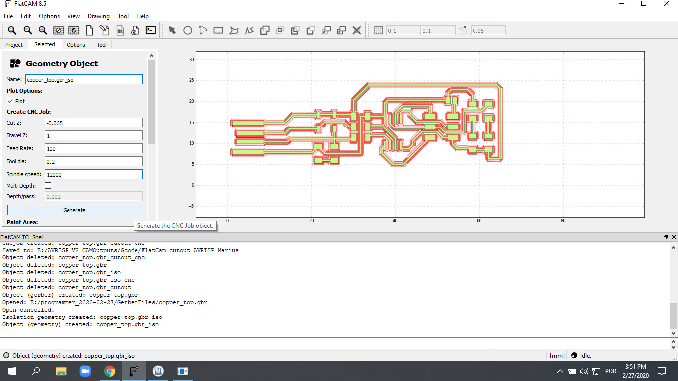
And clicked generate.
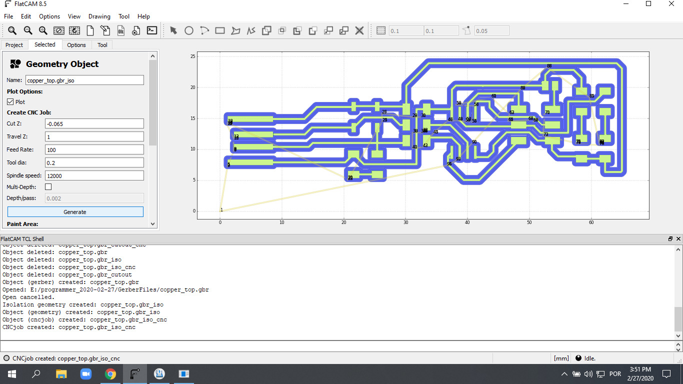
Next step… running the job on the CNC. This was done via ChiliPepper jpadie workspace (Web-based CNC machine management software).
Selecting units in Millimeters.
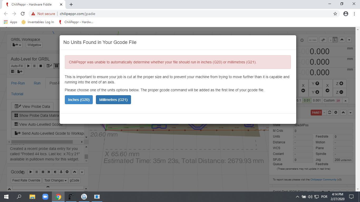
Be sure to have the connection with the CNC working and not locked. And run the auto-level to set a good base for the milling job.
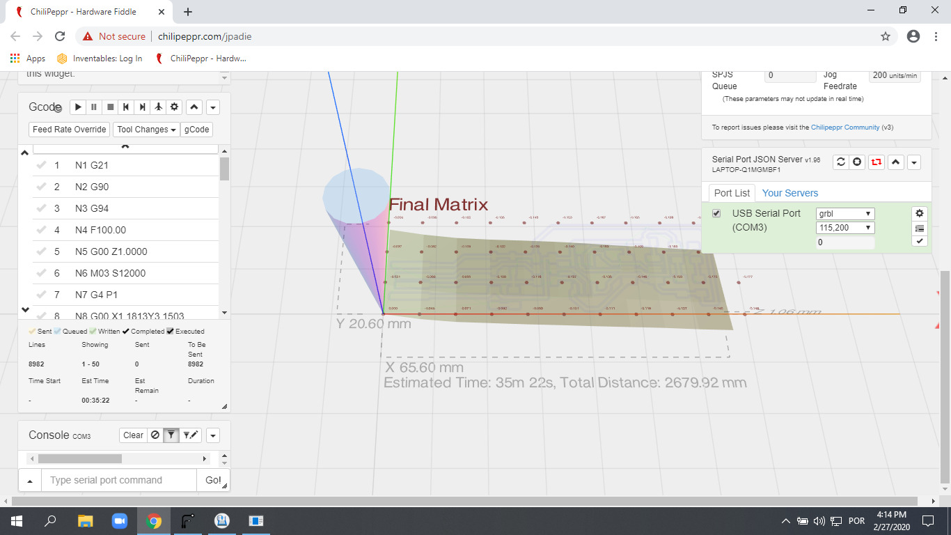
And run the circuit CNC job file!
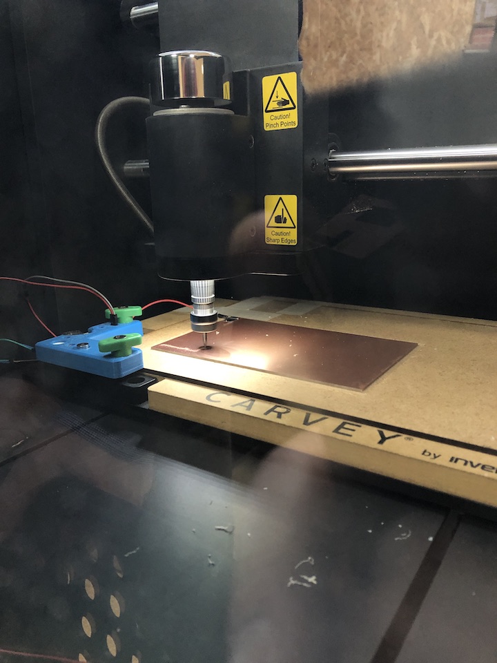
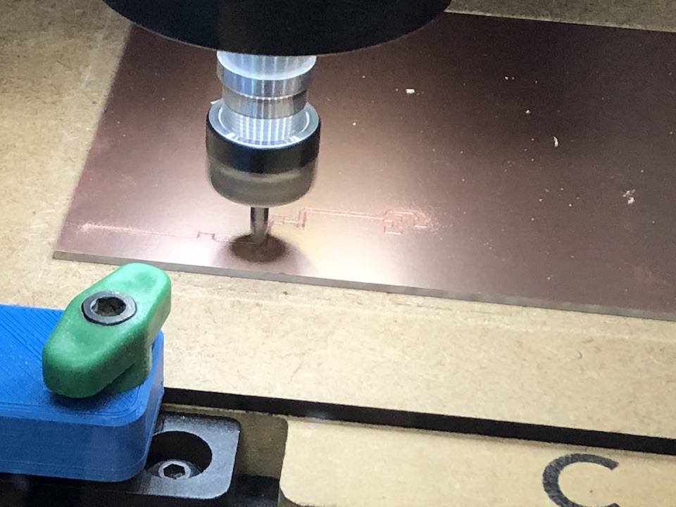
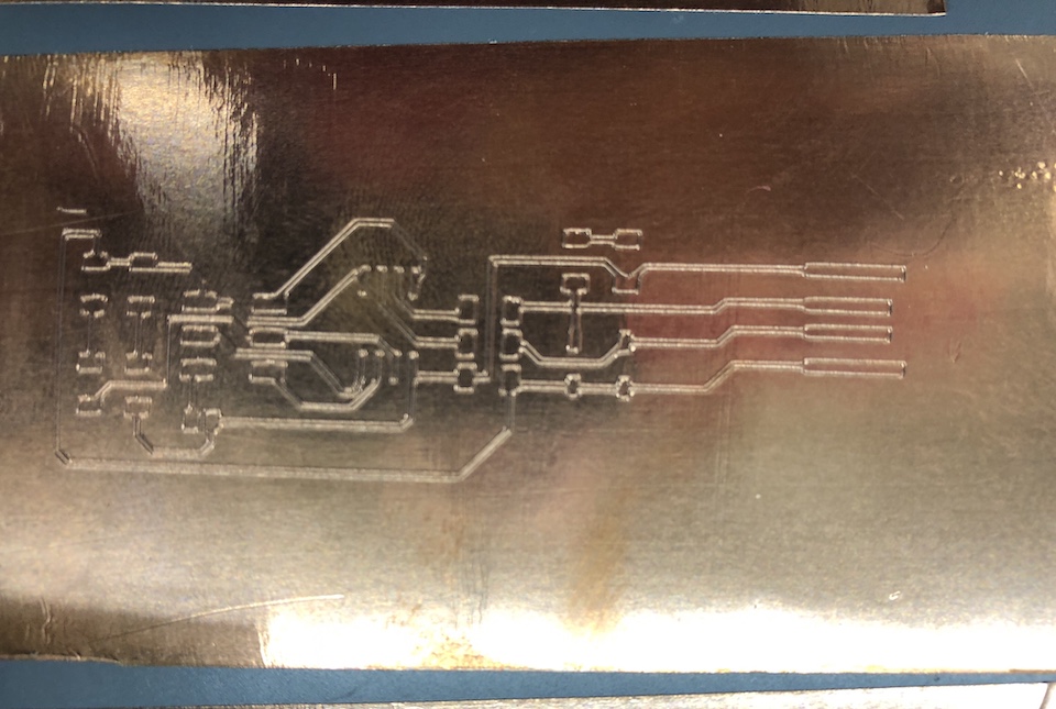
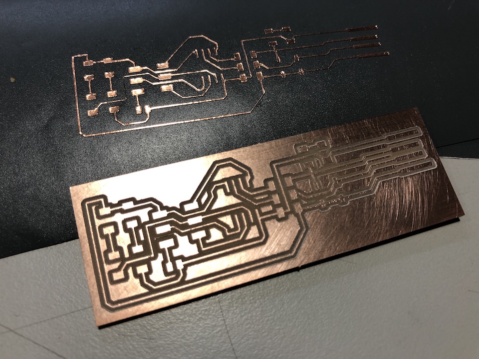
The result after small cleaning looked good.
Next step, the board cut-out. For this it was used a DIA 0.8 endmill, CNC needed to be zeroed again because of the exchange of tool. Returning to FlatCAM the cut-out was prepared. Settings:
- Tool dia: 0.8
- Margin: 2
- Gep size: 0
- 2 (T/B)
and clicked to generate cut-out geometry.
Then last step was to generate the job for CNC with settings:
- Cut Z: -1.8
- Travel Z: 1
- Feed Rate: 80
- Tool dia: 0.8
- Spindle speed: 12000
- Multi-depth checked
- Depth/pass: 3
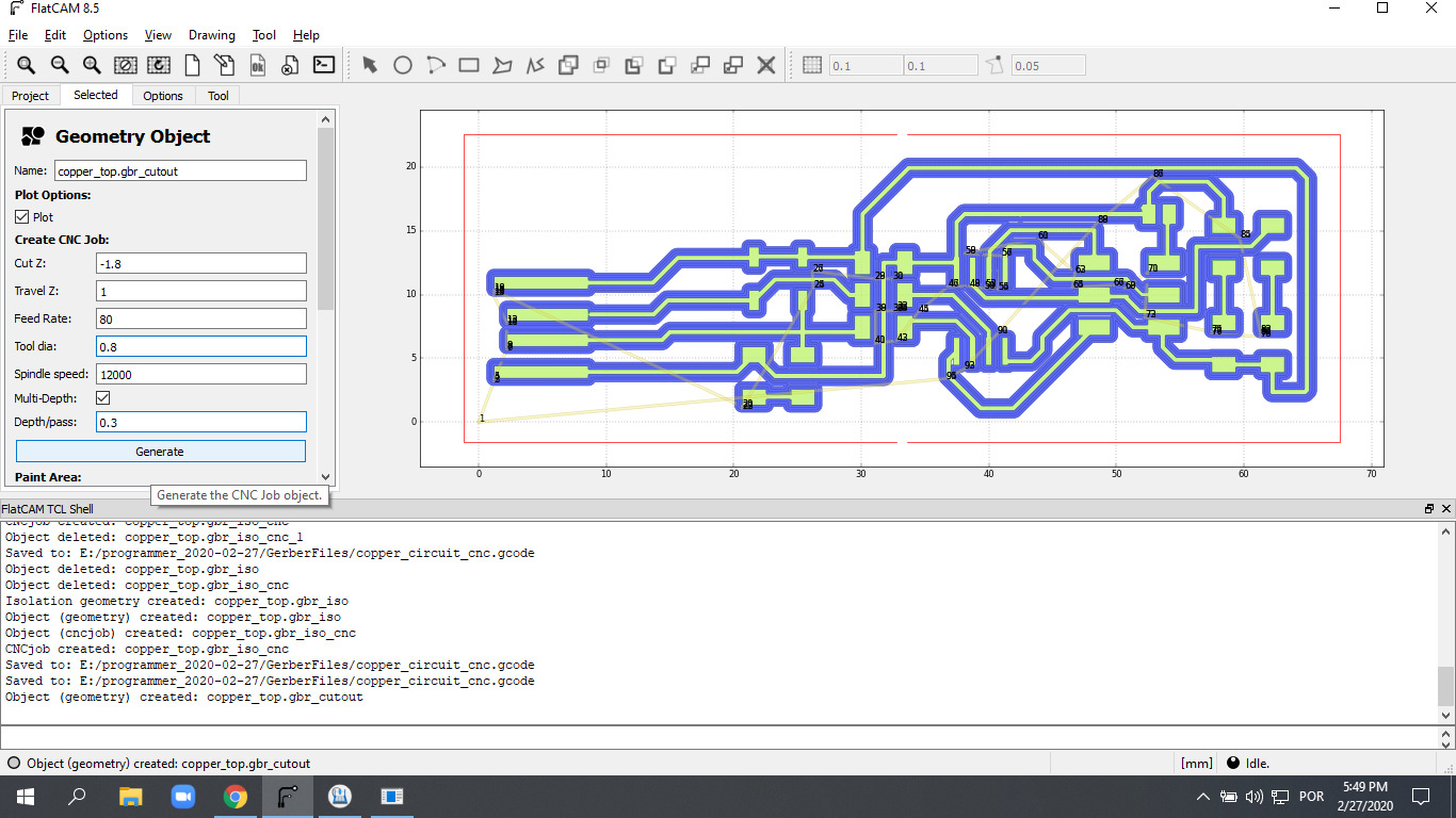
and Generate the CNC job file!
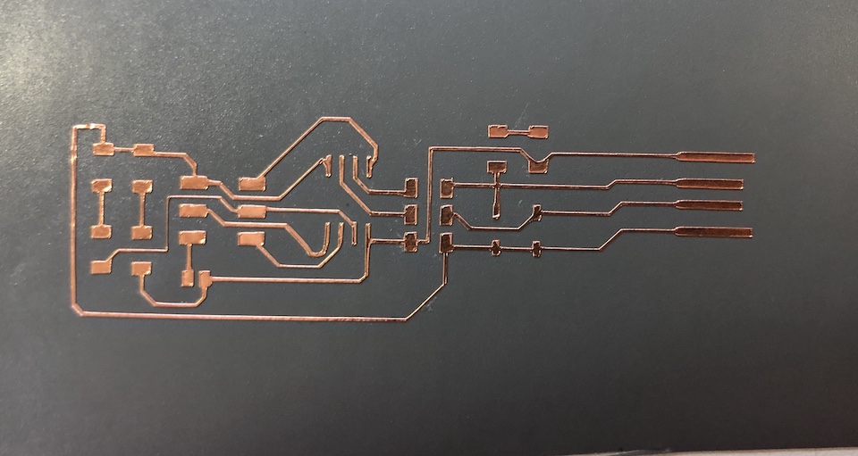
After running the cut-out job via Chilipeppr and removing the PCB from the CNC the result good for me :)
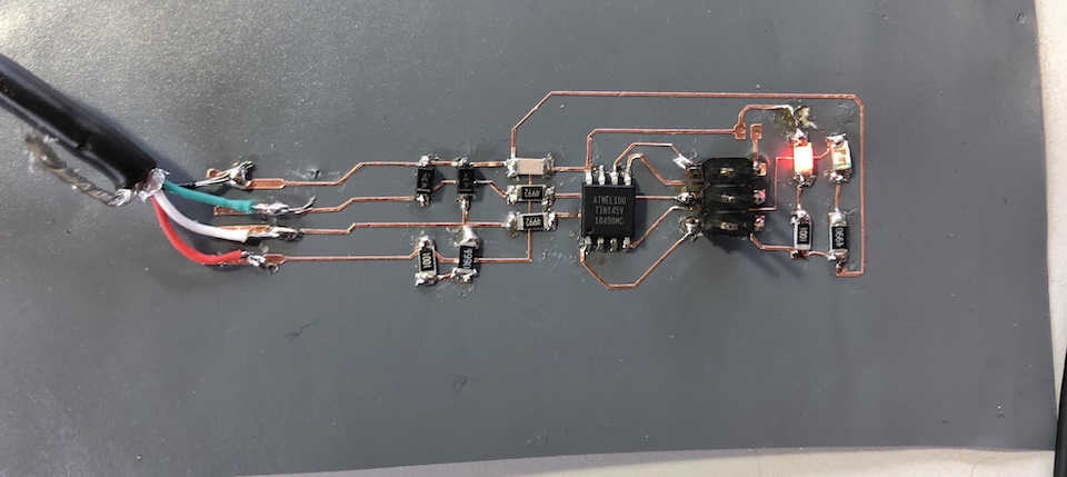
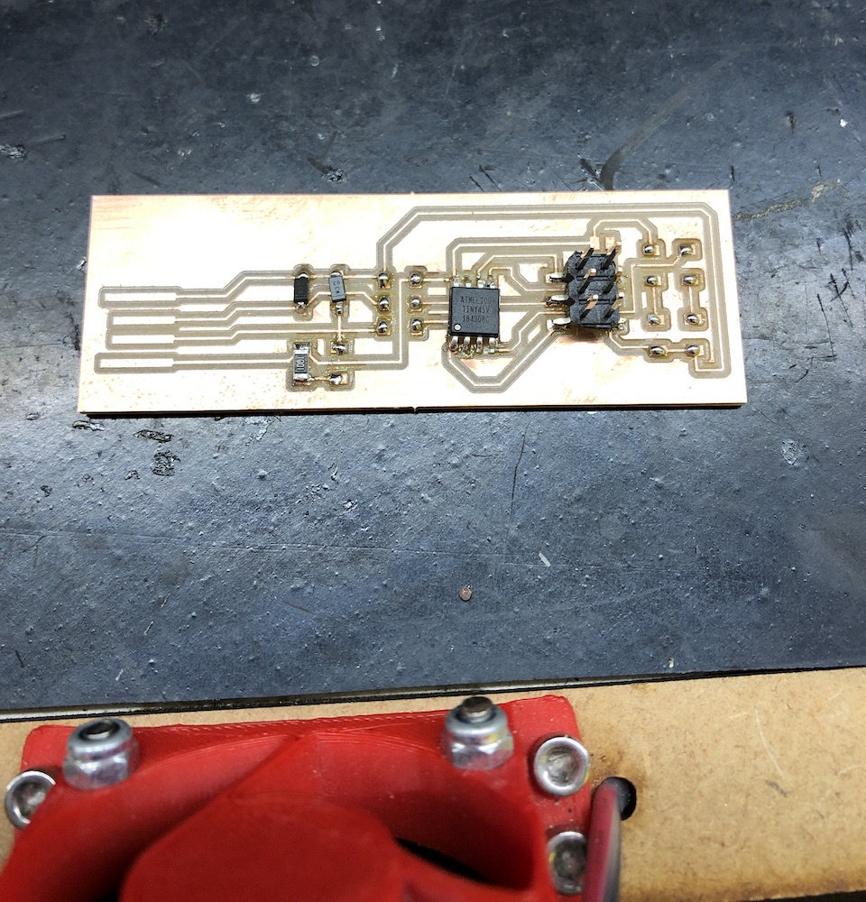
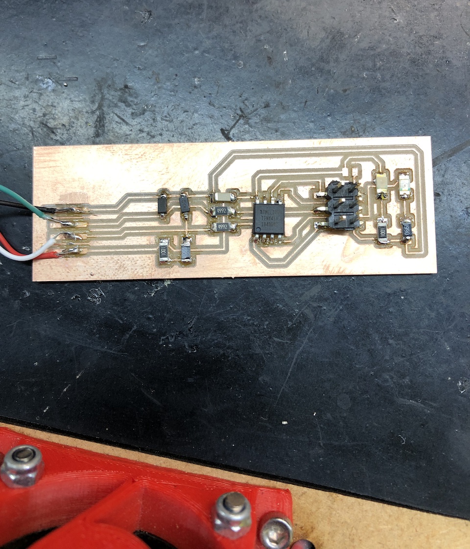
Stuffing the board
While stuffing the board was always checking with the multimeter for connectivity of solder points, components. Did this to try to minimize any mistake during this process. Anyway, mistakes were done while learning to solder, by using wrong resistors, but this was an easy fix, after knowing the problem :)
Programming the ATtiny45
To program the board i downloaded CrossPack and installed the package on my MacOS. Also downloaded the firmware source code, unziped the file into avr directory and run command “make all”. This generated the fts_firmware.hex binary file to program ATtiny45. No changes were needed to do in the Makefile because i’m using the default setup.
To program the board i used another programmer connected to my FabTiny board via ISP connector
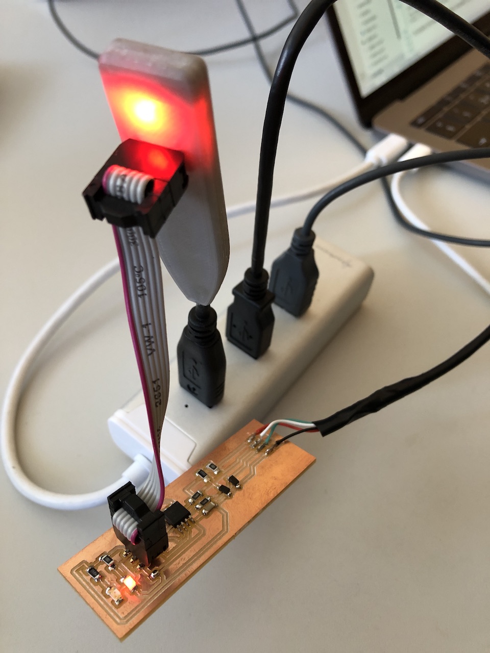
After this i managed to load the firmware into the ATtiny45 by running: “make flash”
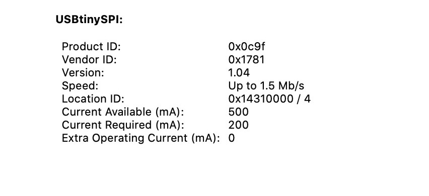
Success! Board shows up in the USB Bus :)
Time to blow the reset fuse. This is done by running “make rstdisbl” and then remove the solder from the jumber on the board