- Design and produce something with a digital fabrication process not covered. Incorporate computer-aided design and manufacturing.
This week I will fabricate a PCB board not by milling, but rather using a new method, etching. It will be the PCB board I plan to use as a gaming controller for a program I created and which I will integrate in the Interface and Application Programming week.
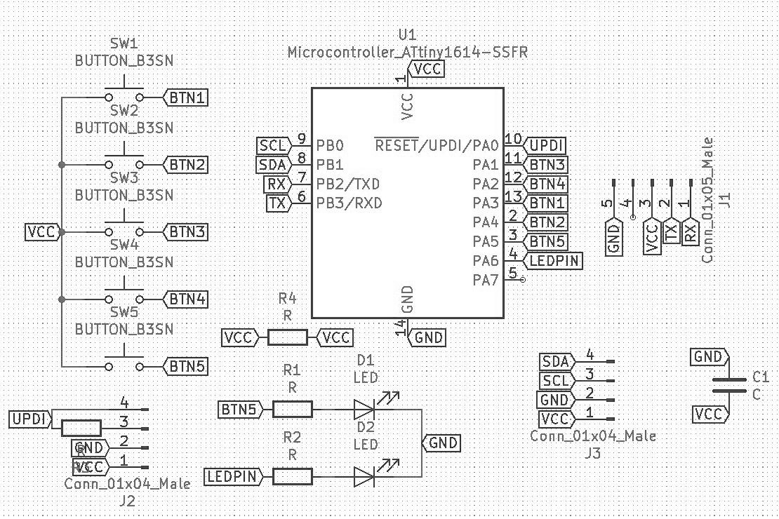
As in prior weeks, I have designed the board in KiCad
As part of the process of etching, my lab uses a UV printer, which is a very versatile way to print almost anything on almost any surface. It just has to fit in the machine. UV printers spray the special ink onto the material on the first pass, then moves back with the UV LED on, which cures the ink quickly. It then moves up and repeats the process. It’s a really nice way to print, not just limited to paper.
I’m using a Roland Versa-UV LEF-12i printer using the Versaworks software. You need to upload a PDF to the Software. So, after exporting the SVG from KiCAD, I use CorelDraw or illustrator to change the format to pdf mantaining a high resolution. When changing formats from svg to pdf I need to be very careful to maintain the same aspect ratio and size, or it will mess up the print and the components would not be able to be soldered on.
Once I upload the file to Versaworks, I need to change the settings, so that the intensity of the black ink is set to 100%, and make sure the PDF is not scaled. Next, I have to set the height, width and length of the object, this is done directly on the machine, using the setup button while moving the printer head to establish the dimensions. Then, on the Versaworks, you need to click ‘Get material sizes’ on the software.
Once that is done the machine should have the ‘Ready to print’ status. Then, you click print on the computer, and it starts the printing. Stay next to the machine to make sure everything is right but be careful not to look directly when the UV LED is on. This can damage your eyes. So, look when it’s spraying the ink, but not when the UV light is on.
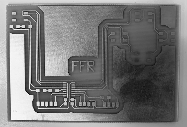
I would like to etch my final board and my interface and Applications board. It’s a new process that I have never tried before and it seems to give a crispier result of the traces than milling. It seems to give a more professional and cleaner look to the PCB, something I like.
So, as I said above, I exported the SVG from KiCAD and then set up the printing on Versaworks, as in any print setup.
I quickly found out that I had to prepare my board before printing. The boards I am using are not of a very high quality copper. And in the first few tries it was something that greatly affected the way the ink adhered to the surface. Additionally, I had to make sure that I did not leave the board too long in the acid so it would not eat away the surface. So, I first cleaned the copper surface with IPA, isopropyl alcohol, and then sanded it a bit making sure the patterns are random. The sanding was as a method to improve the adherence of the ink to the copper surface. Once that was done, I placed it on the printer bed and clicked Print.
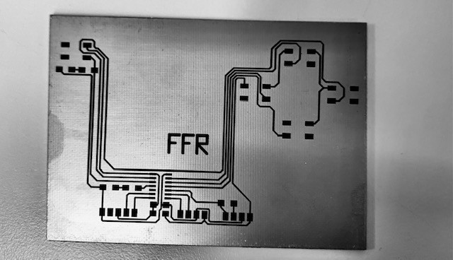
On my first print, I didn’t offset the traces at enough distance from each other, making them too thin and too much copper around the traces. Since the acid takes longer to eat all the excess copper, the acid was destroying the thinner traces. So, I drew some square around my traces in CorelDraw in order to reduce the printing area. In order to re-use the same board, I removed the ink of the previous print with some acetone, then I cleaned it with IPA and printed the new version before placing it in the Acid.
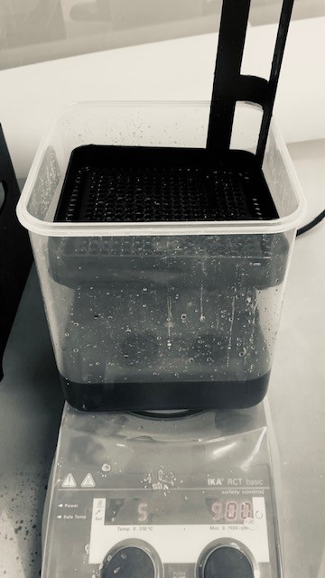
As the acid can eat copper, it can also quite easily eat your skin away, so it is very important to stay safe and were gloves, a lab coat, eye protection, and have good ventilation in the area you are woking. I’m working under a fume exhaust cabinet which only let’s my hands through (with gloves obviously). For greater efficiency, I’m using a stirrer/heater device than stirs and heats the acid while it’s eating the copper. The striring and heat combination makes the process faster. So, I put it in, and left it for 15 minutes.
However, due to my inexperience, I did not sand the copper enough and left it for way to long in the acid. I removed it from the acid, the ink was all wrinkly and it did not look good. It also left some copper around my initials.
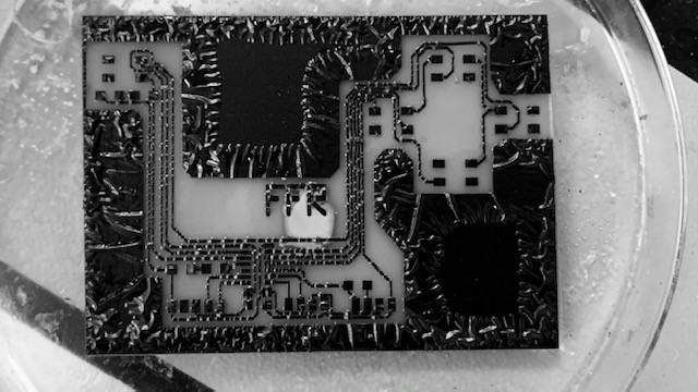
I still thought it would work but after removing the ink with acetone, yeah, no.
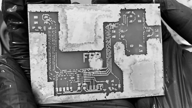
I got another board then cleaned and sanded it. Next, I printed the design on it and placed it in the acid. I decided to check frequently and got it out at the perfect time. I removed the ink with acetone and brought the clean board home! Then, while soldering I proceeded to burn a pad off immediately. Oh well, more practice for me.
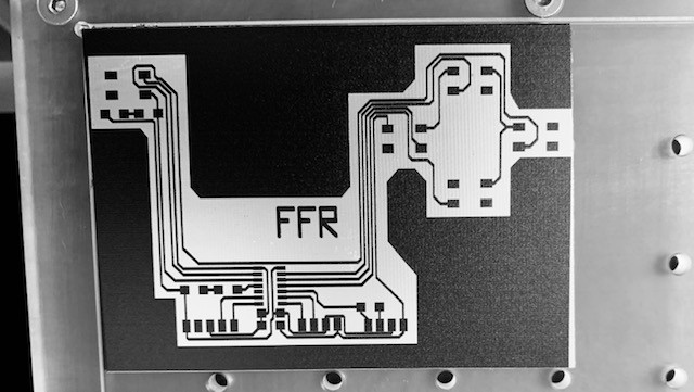
So, I printed a new one, this time, I made the extra copper directly in KiCAD so it’s smoother and nicer looking. I sanded it better and sent it to print. Then, I carefully placed it in the acid and checked every 2-3 minutes on its progress.
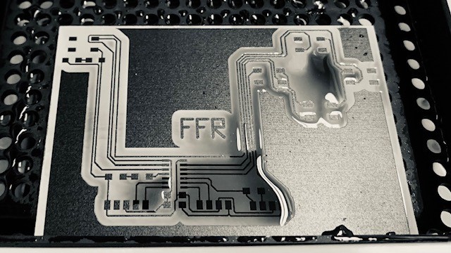
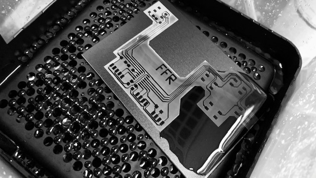
After removing the ink with acetone, I looked onto the perfect, crisp, and incredibly smooth board that I made. I was amazed by the incredible results. I definitely will use this process more often.
It was a very nice experience to fabricate something as a PCB board by combining printing and a chemical process.