Table of Contents
Assignment Designing the PCB Designing in KiCAD Milling the PCB Stuffing the PCB Design Files^
- Use the test equipment in your lab to observe the operation of a microcontroller circuit board.
- Redraw an echo hello-world board.
- Add (at least) a button and LED (with current-limiting resistor) check the design rules, make it, and test it.
- Extra credit: simulate its operation
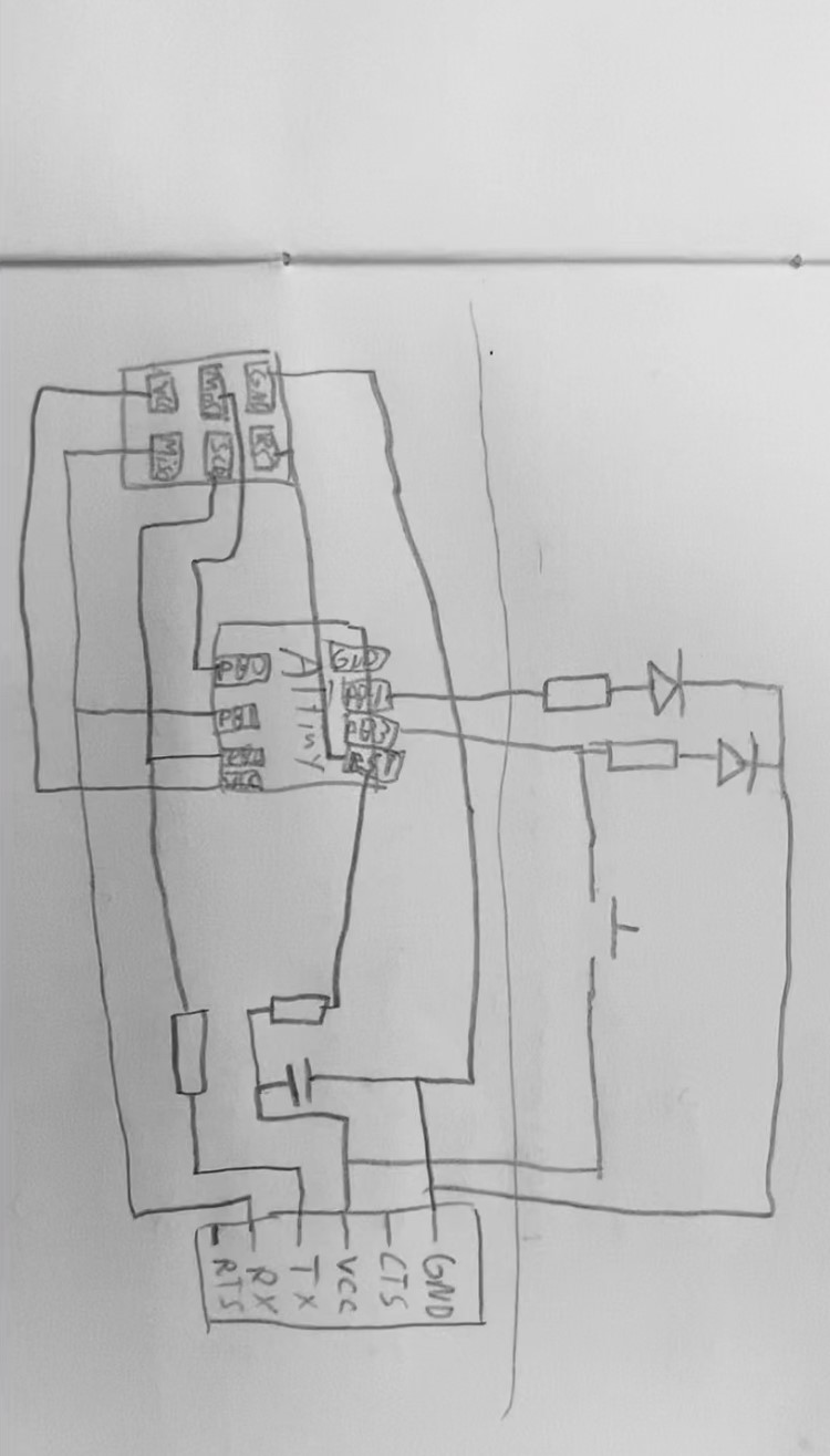
This week, we need to design a printed circuit board with a microcontroler. After discussing with my instructor we eventually settled on using an ATtiny 45, adding a button, and two LED, one red and one green. The red LED will receive the instructions of the program from the ATtiny and the other will turn on when the button is pressed activating the program that lights up the red LED. Electricity will flow into the ATtiny's designated Pin and then that would make the red LED flash in a pattern according to the program. In order to start designing the PCB board, I drew a quick sketch with the circuit layout idea.
The sketch helps me visualize the circuit in order to start designing it in a CAD software. I downloaded EAGLE using my Autodesk license from FabAcademy, and opened it up. I found the software weird, not very user friendly. I was just messing around a bit, but I couldn't get anything to work. It felt un-natural and strange. I tried searching for help or tutorials but all I could find was a severly outdated video that was 10 years old. I also tried doing it in Fusion360's Eagle version, but there was no help tutorials to be found.
1 - Download the Library as a ZIP file. Open it and copy it's path.
2 - Open KiCAD
3 - Click on preferences, and on Manage Symbol Libraries. Add a new library, by clicking the plus symbol, and paste the path you copied from earlier then add the file at the end, it has to be the file not the folder.
4 - Now open Manage Footprint Libraries in preferences. Add a new library the exact same way as before.
5 - Open Configure paths in preferences again. Add a new variable, this time the path is the folder, not the file.
After getting the library dowloaded, I opened the tutorial again, and started designing my board with its help. I didn't do all the specific details needed for a Boardhouse, but nevertheless I quickly got my Schematic complete.
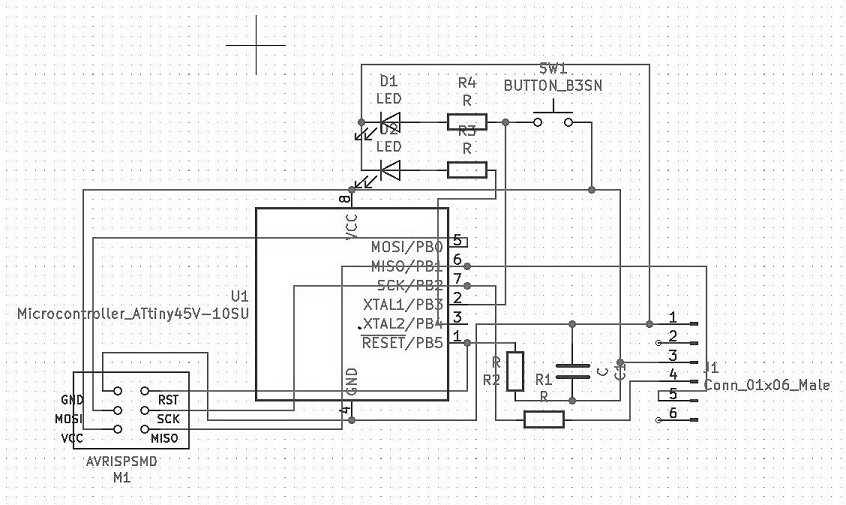
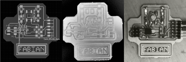
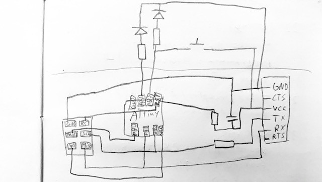
After completing the schematic, I needed to design the circuit's traces. I opened the file in KiCad again, and updated the parts. Then I started arranging the components, trying to get a layout design that worked and was as compact as possible. All the designs that I tried didn't work properly. I spent hours obtaining terrible trace designs, until I finally decided to take a look and base my design on Neil's design. I looked at his echo hello board design, and found that I could easily add my button and LEDs right above the pins 3 and 4. There was a nice empty area there. So I re-arranged my components into a similar layout to Neil's, and added one button and two LED above. I wired up the parts, and sometimes would find an issue with my schematic design. Luckily, whenever you updated the layout it didn't remove anything you did, so I could easily update and fix errors. I added a circular outline and with that edge it was done. I even added my initials on the bottom. I would show it on my regional review meeting and then mill it the next day.
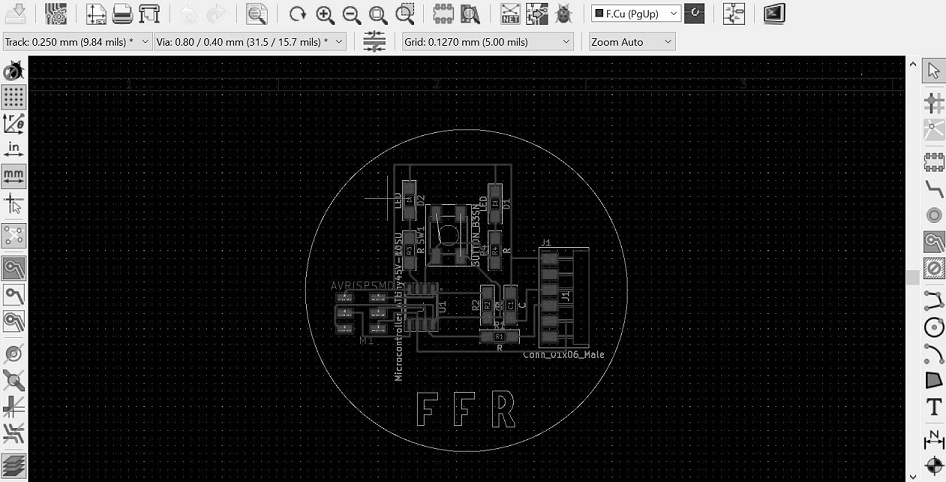
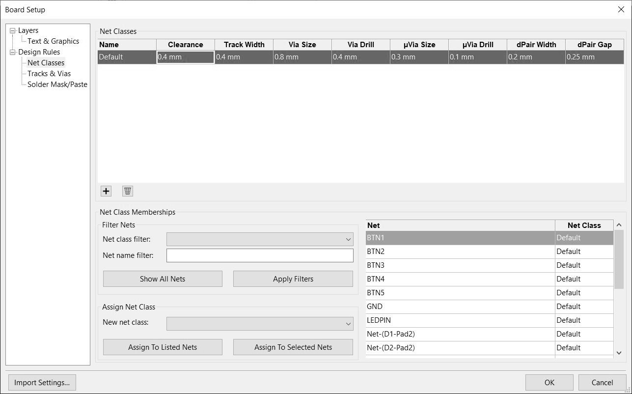
When presenting at the regional review, it was remarked that my traces were too thin. I had to modify them with a suggested clearance and trace width of 0.4 mm's thick. I edited this within the design rules as I expected the design rules to update my board, but no, it did not automatically update so, I had to delete every trace, and redraw them.
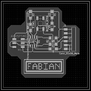
Eventually I updated my design, and I got my layout completed! I added my name on the bottom as well. Now I needed to upload it to Mods. I was using a tutorial from Aalto fablab which explained how to do it, I also reviewed Neil's lecture, because he explained a trick to export the outline edge to Mods. When reviewing the class' lecture I learned that I had to draw the outline on the B.Fab layer, and export is as the technical layer to dodge some issues later on from Mods. The tutorial from Aalto also mentioned making a margin. So I made the margin, and the circle in the B.Fab layer.
But it did not work when exporting to mods. It had to be a polygon, who's background was completely filled in. I couldn't make a circle, as the polygon tool worked only with straight lines, so I made a plus shape. I removed my initials and wrote my name using traces, which looked cooler and worked better.
I then exported it as an SVG and opened it in Mods. I used the same tutorial as last time when milling, and exported it to be cut in the Roland milling machine.
Given my experience from the Electronics Production week, the milling of this board was quite srtaight forward.
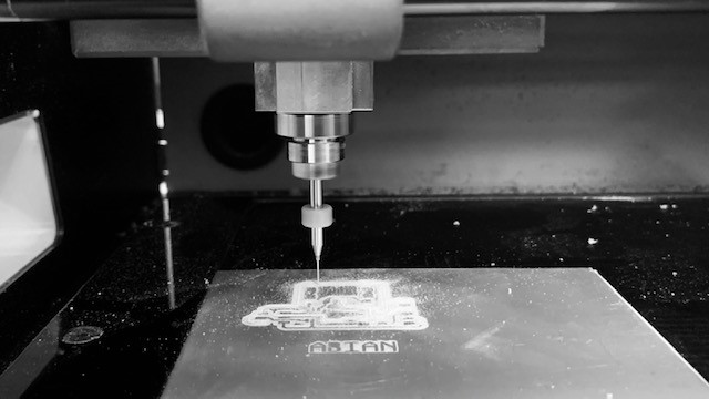
I prepared the milling files in Mods and opened them in the Roland milling machine. I determined the 0,0 location for the X and Y axis. Using the .4mm milling bit I proceed to mill the traces of my PCB board.
After milling the traces I changed the milling bit to an 8mm milling bit in order to mill the outline edge.
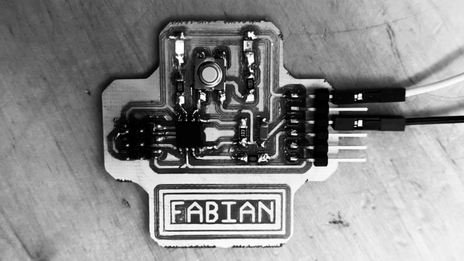
Now that my Echo Hello Board is milled I need to "stuff" it. In other words, solder the electronic components onto the milled board. The component list that I am using in my board are the following:
1 - (1) ATtiny 45
2 - (1) Red LED
3 - (1) Green LED
3 - (1) Button
3 - (3) 1k Resistors
3 - (1) 10k Resistor
3 - (1) 1uF Capacitor
4 - (1) 6 Position 2 x 3 Header
5 - (1) 6 Pin 1 x 6 Header
I soldered all the components, starting with the ATtiny, working my way outwards and finally the two header connectors. After soldering all the components, I then checked with a multimeter for any shorts, thankfully there were none. At last, here is my "stuffed" PCB board ready to be programmed!
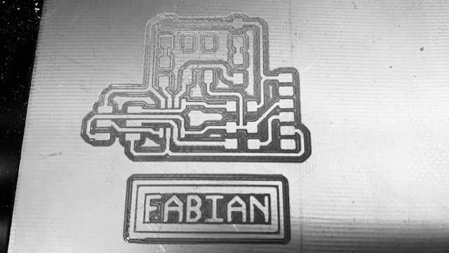
Echo Hello Board Traces
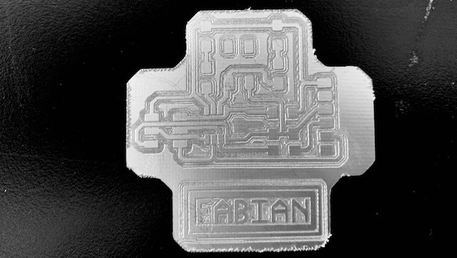
Echo Hello Board Outline