Individual Assignment
This week's individual assignment includes:
● Redesign an echo hello-world board:
add a B3SN-3112P button and a LTST-C150CKT LED
● Fabricate the board
● Program and test the board
Board Design
Board design is accomplished with AutoDesk EAGLE.
Environment Configuration
Language Setting
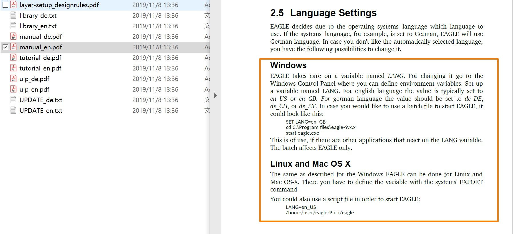
By default, the operation language of EAGLE will inherit the language of the local operation system. If the users want to change the settings, there is a tutorial in the EAGLE folder, doc>>manual.pdf>>2.5 Language Settings In my case, because I use Windows 10 system, so I just set an environmental variable called LANG and then save a .BAT file that contains the following code or run these code in the Command interface
SET LANG=[language name]
Then the language are set to language that the user want.
cd [root folder]\eagle-9.5.2
start eagle.exe
Libraries and Design Rules
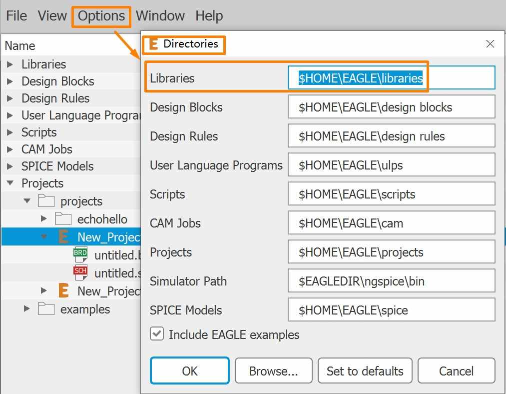
Several EAGLE Libraries and design rule files need to be downloaded and added to EAGLE's Libraries folder.
● fab.lbr
● ATTINY412-SSF.lbr (if not included in fab.lbr)
● fabcity-designrules.dru
Both methods can help you add these files to EAGLE libraries folder:
● Copy the lbr files to User>> Document>>EAGLE >>libraries
● In Options >>Directories, change the Libraries directories to your preferred folder
Schematic Design
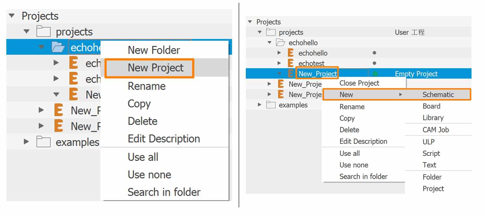
First, creating the schematic interface via File>>New>>Project. Then right-click the project and create a new schematic by New>>Schematic
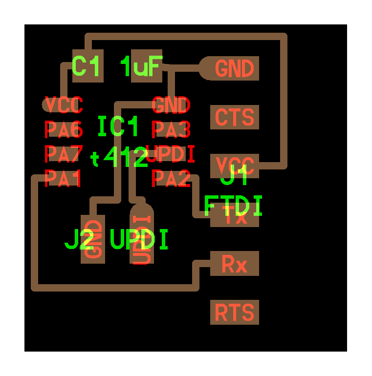
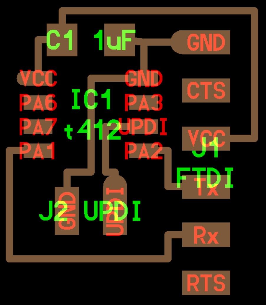
The schematic design task will be based on a ATTINY412 echo hello-world board, while a press button switch and a LED will be added to the original design.
The schemes of the following parts are required for this board:
● ATTINY412-SSF
● CONN_06_FTDI-SMD-HEADER
● CONN_03SMD_RA_MALE/FEMALE
● LTST-C150CKT LED
● B3SN-3112P Button Switch
● R1206FAB(499Ω)
● R1206FAB(10KΩ)
● Capacitance(1u)
● GND*5
● VCC*4
1. Add the necessary parts
To add component to the canvas, use Add Part on the side tool bar.
-Directly clicking the icon allows the user to add the part by libraries
-Right-click the icon or clicking the little triangle on the right botton corner of the icon provides the users with a shortcut to add recently used parts.
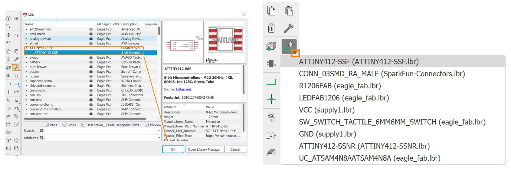
In this process, the capacitance should be set to 1 u and the two resistances should respectively set to 499Ω and 10kΩ. Right click the part and select Value will allow users to set the value for that electronic component.
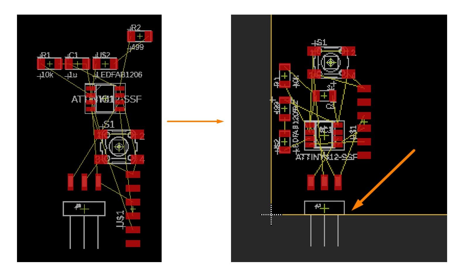
2. Connection and Layout
After adding the parts to the canvas, connect the parts based on the original echo board with the Net tool on the side tool bar.
While connecting the parts, it may be helpful to move or rotate the parts to make the circuit less complex or less tangled.
- To move or rotate a part on the canvas, click the corresponding icon on the side menu bar and overlay the cursor on the "+" sign of each part, then the users can move or rotate the part freely.
- Click the Group tool and right click the selected parts allows users to accomplish group move or group rotation.
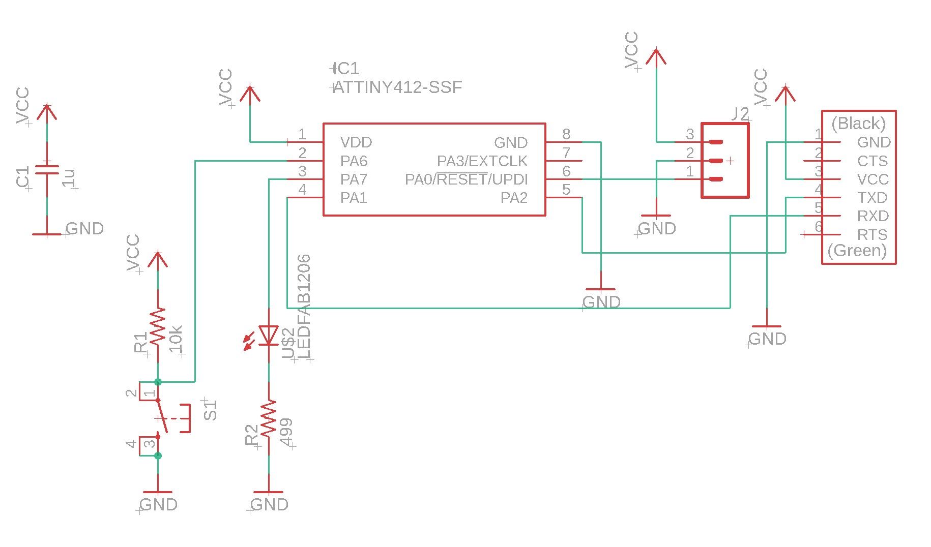
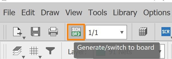
After finishing the schematic design, click the Generate/Switch board icon on the top tool bar.
1. Drag the components to the canvas
2. Adjust the layout and orientation of the parts
- Similar to schematic design, to move or rotate a component, users just need to overlay the cursor to the "+" sign and the corresponding item will be moved on the canvas.
- The goal is to make the connections between parts as simple and straightforward as possible
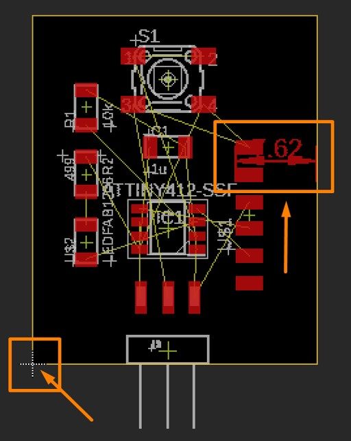
3. Adjust the board size
- Adjust the canvas to fit the size of board
- Set the line width to 16 mil
- The two connectors must be placed at the edge of the board
* CONN_03SMD_RA_MALE/FEMALE should be placed at the bottom edge
* CONN_06_FTDI-SMD-HEADER should be retain a distance of 7.62 mm to right edge
4.Route the Wire
* The connection between components are labelled by thin yellow lines
* Press Alt button will allow users to make finer adjustment
* For aesthetic consideration, avoid right angles .
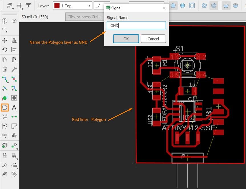
5. Create Polygon
- Use the Polygon tool to create a polygon that covers the entire board
- Name the polygon as GND
*This create a ground pour, and is done as the last step after routing the signal wires.
6. Ratsnest
The tool ratsnest recalculates the minimum distance of the wiring, and also generates copper areas defined with the named polygons.
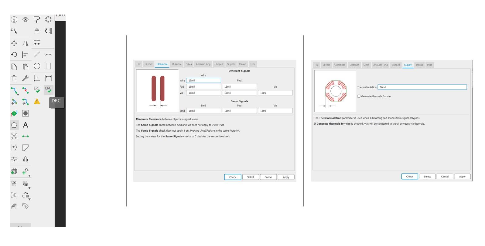
- Before ratsnesting the board, change the Design Rule settings with DRCtool in left tool bar
* If the DRC icon cannot be found, maximize the interface and it will be shown in the collapsed menu
* Change all parameters in Clearance and Supply tab to 16 mil
- Use the Route tool on the side too bar to wire the components that should be connected
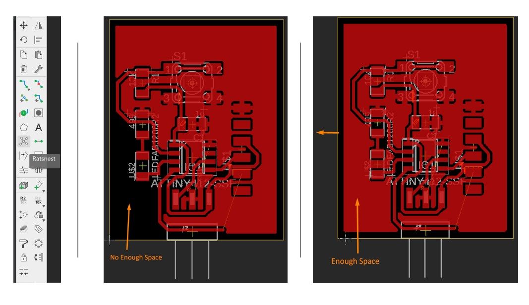
- Use the Ratsnest tool to generate the pattern of copper layer
- The copper layer will not cover the areas with inadequate space
* Resize the board or reroute the wires can solve this problem
- To remove the ratsnest layer, type ripup GND in the command line
7. Design Rule Check
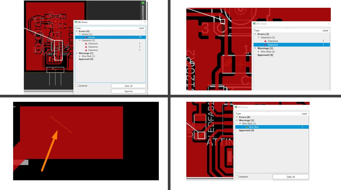
- Click the DRC tool in the left tool bar and click Check
- If the components are not wired correctly, error message will pop out
* Airwire errors indicate the corresponding components are not properly connected
* Clearance errors indicate the corresponding routes are too close
* Wire Stub warnings indicate there are overlapping routes
- If the components are connected perfectly, nothing will happen
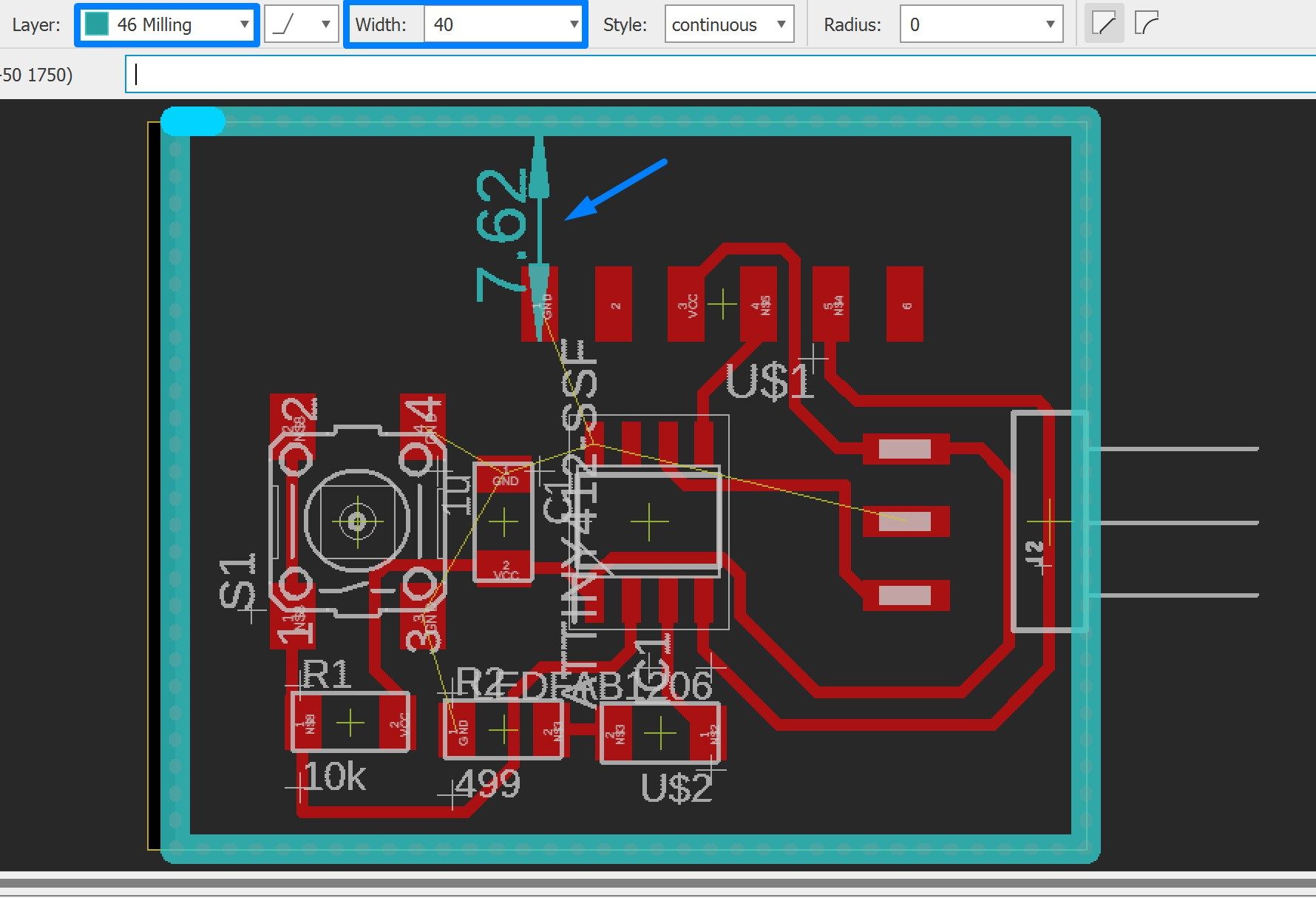
8. Draw Milling Layer
- Switch to Milling Layer (46) and set the width to 40 mil
- Use the Line tool to draw the outline of the board
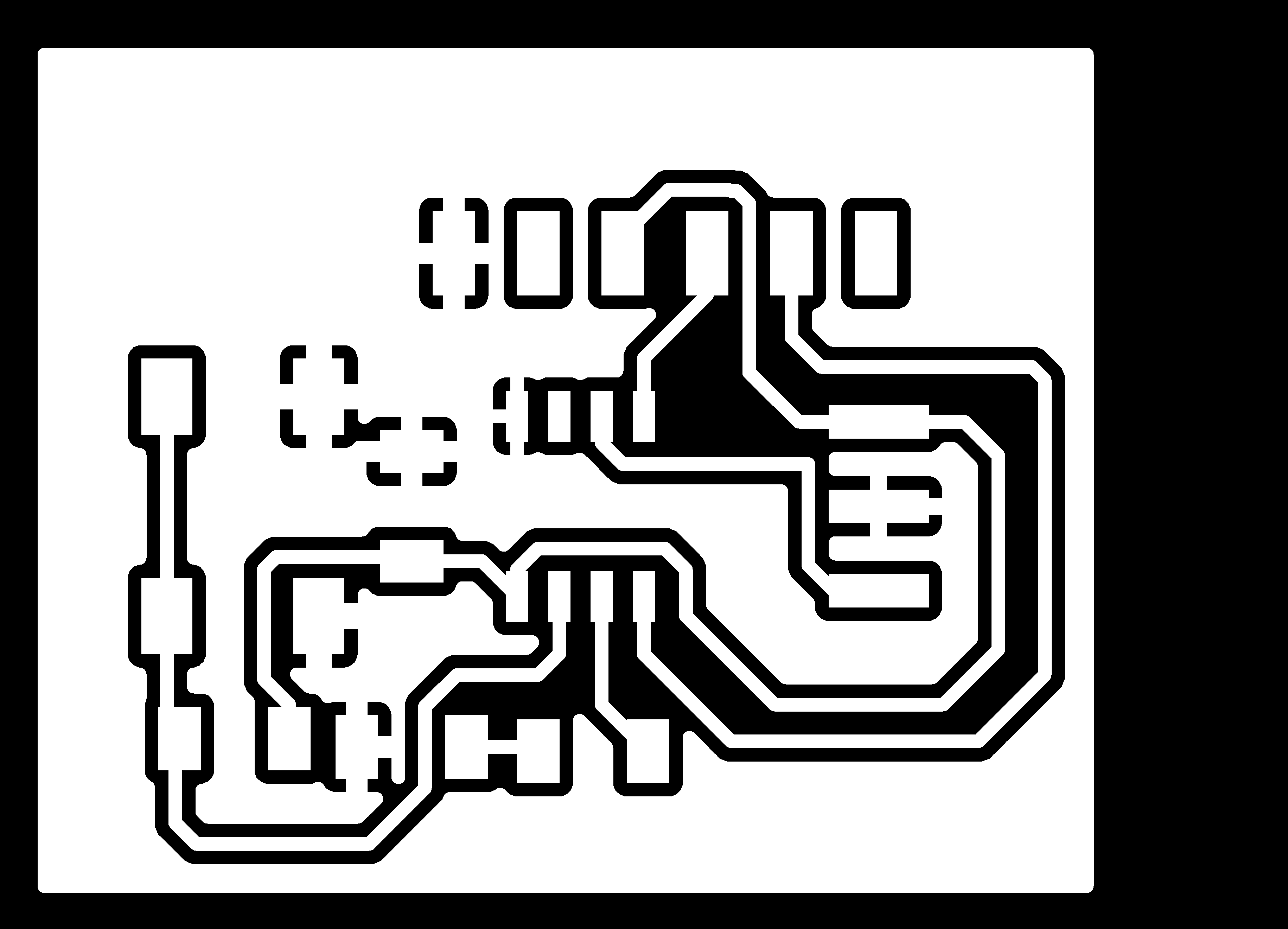
9. Export Image
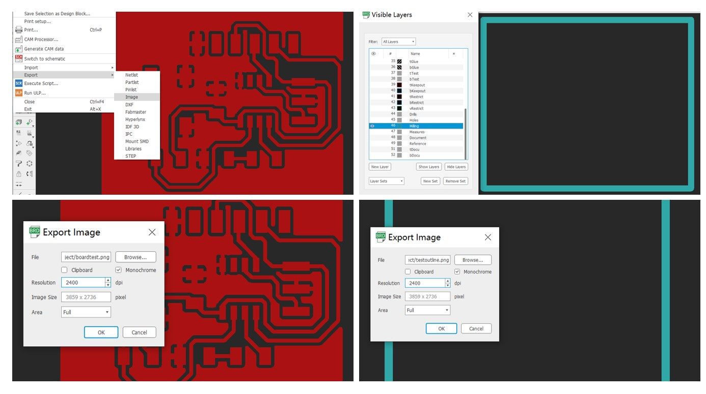
a. Export Board Image
- Select the visible layers as #1 Top
- File>>Export
- Select monochrome
- Set Resolution to 2400
b. Export Outline Image
- Select the visible layers as #46 Milling
- File>>Export
- Select monochrome
- Set Resolution to 2400
* If the exported images are in wrong size, go to Options>>User Interface to uncheck the options in Display section, which will autoscale the image.
The exported images are ready to be upload to Mods
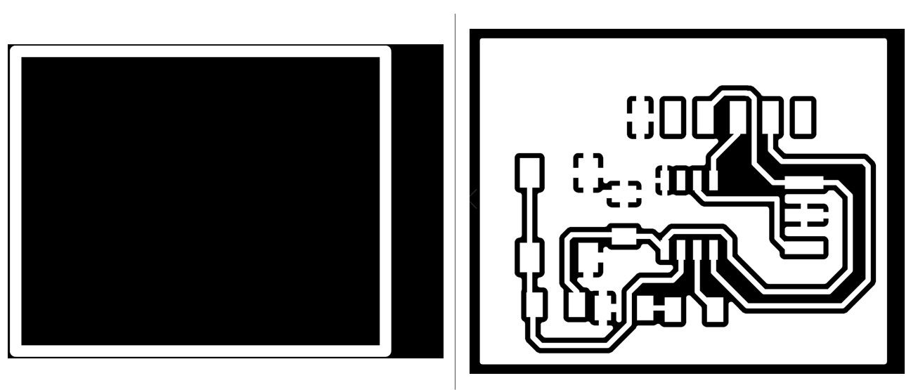
* The outline image needs to be inverted. Copper is always white in these pictures.
- This can be either done during export or when uploading the outline image to Mods. In my case, I invert the color when uploading the png file to Mods.
Board Fabrication
The process of board fabrication is similar to Week 4 Electronics Production, so less details will be contained in this week's document.
Generate Rml files
1. Setting up Mods
- Right Click >> Programs >> Open Server Program >>SRM-20 >>PCB png
- Delete "WebSocket Device" module >> Right click >> modules >> open server modules >> file >> save.
2.Generate trace image
- Upload the board image without inverting
- Mill trace (1/64)>>tool diameter=0.4mm>>offset number=4
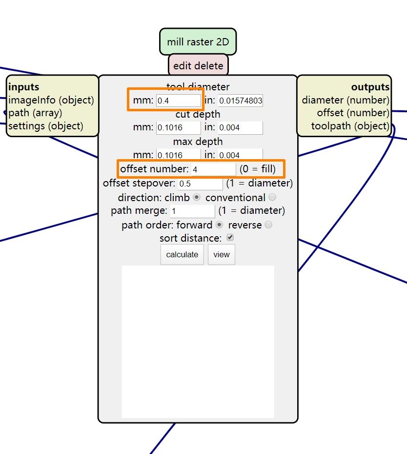
-Calculate and save the rml file.
3. Generate outline image
- Upload the outline image and invert
-Mill Outline(1/32))>>tool diameter=1 mm>>offset number=1
-Calculate and save the rml file.
Mill the Board
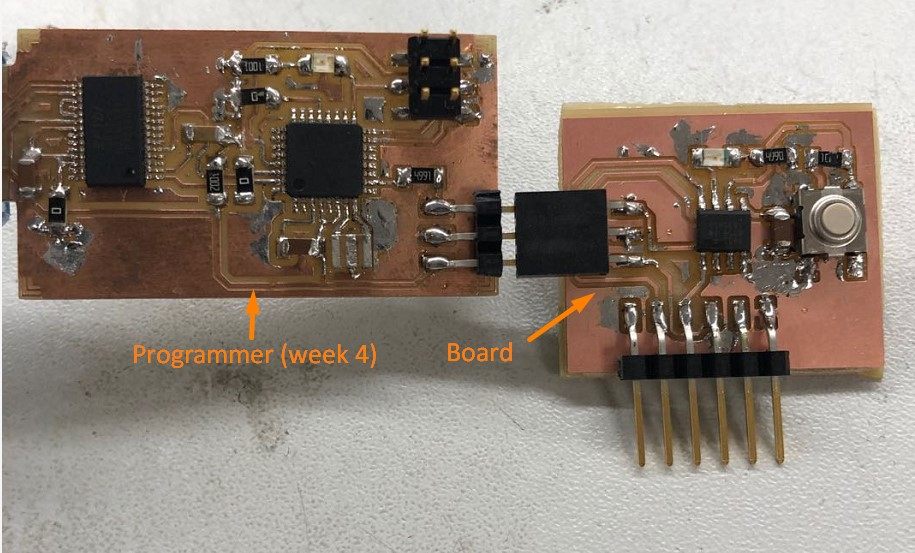
The board is milled with a Roland SRM-20 milling machine.
The trace is milled with a a 0.2 mm - 0.5 mm V milling bit and the outline is milled with a 1 mm milling bit. The process is identical to Week 4 Electronics Production, please check that week's document for more details.
Solder the board
1. Collect the following parts
● ATTINY412 Chip
● 6 Pin Header
● 3 Pin Connector-FEMALE
● LED
● Button Switch
● Capacitance(1u)
● Resistance(499Ω)
● Resistance(10KΩ)
2. Solder the part onto the board
The operation is identical to Week 4 Electronics Production, please check that week's document for more details.
Programming and Testing
The process of programming is similar to Week 4 Electronics Production, so less details will be contained in this week's document.
1. Upload echo program
- Connect the board to the programmer that was made during Week 4 and the computer
- Run Audrino and upload the echo program to the board following these steps
*Tools>> Board: "ATtiny412/402/212/202"
...Default Settings...
Port: [The corresponding device]
Programmer:"jtag2updi(megaTinyCore)"
*Top Menu Docker >> Upload
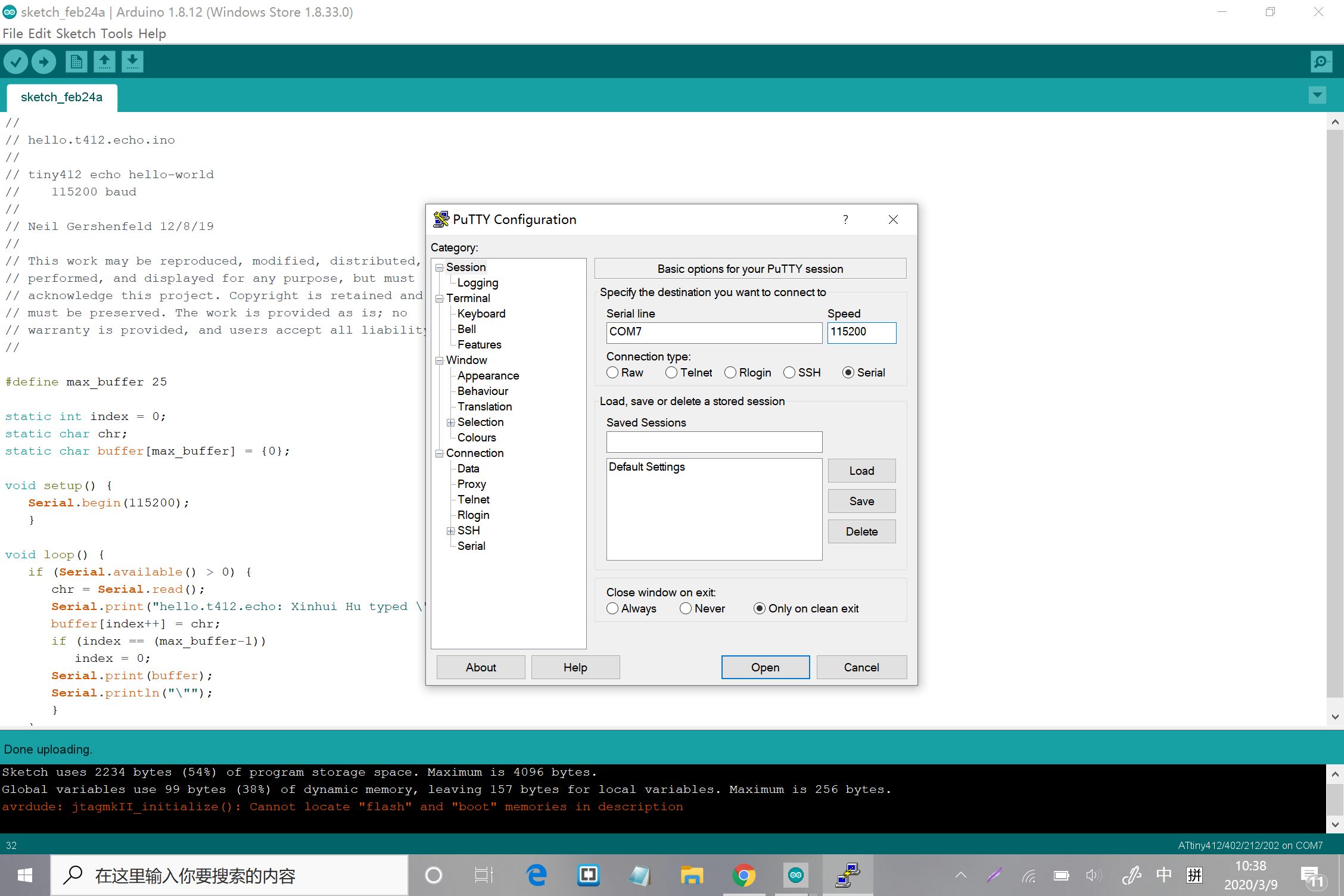
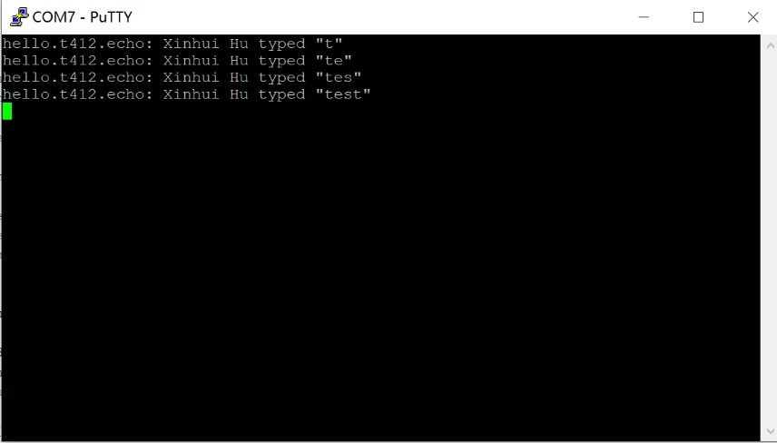
2. Test the program
- Connect the board to the computer with a 6-pin wire
* The ground pin is usually labled black, which helps to determine the direction of the board.
- Run PuTTY, select serial mode with the following parameter
* Serial Line -> [Corresponding Port], which is COM 7 in this case
* Speed -> 115200
- If the board achieves its function, an interface will pop out, which will record the characters typed by the user.
Further examinations of the board have been conducted in the group assignment.
Group Assignment
The group assignment of week 6 focuses on testing the operation of the microcontroller circuit boards that we made in the individual assignments. Please check our Group Assignment Page for more details.
Files
EAGLE Files:
● echo schema.sch ● echoboard.brd
PNG Files:
● Trace.png ● Outline.png
RML Files:
● Trace.rml ● Outline.rml