Group Assignment
The group assignment of week 4 focuses on characterizing the design rules for our PCB production process. Please check our Group Assignment Page for more details.
Individual Assignment
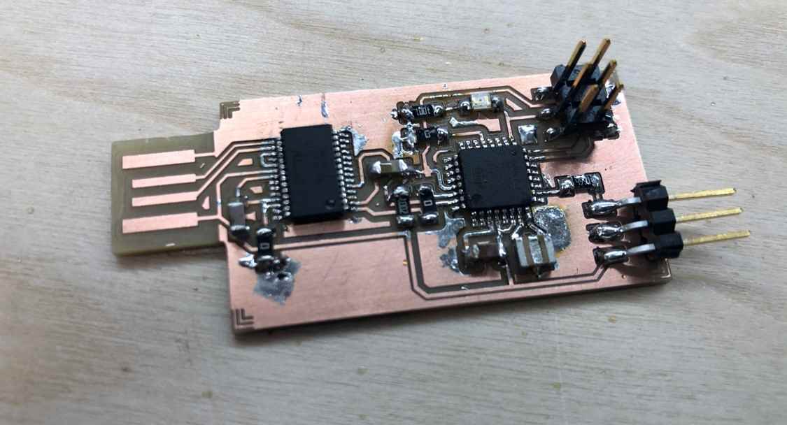
The individual assignment of this week mainly focused on making a updi programmer from sketches, which involves processing trace patterns, milling PCB board, soldering electronic components, programming and testing.
Trace Generation
File Retrieval
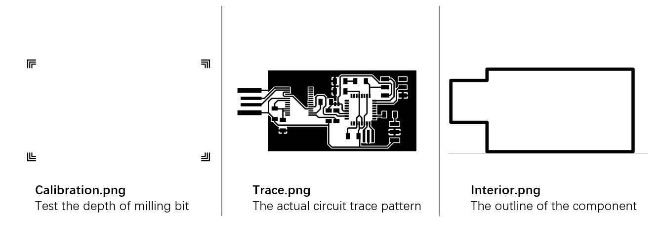
Three trace files need to be accessed via GitHub and processed for PCB milling:
● Calibration.png
● Trace.png
● Interior.png
Trace Process
These files will be processed by an online processor, mods.
1. Pull up the processing interface via the following path:
Right Click >> Programs >> Open Server Program >>SRM-20 >>PCB png
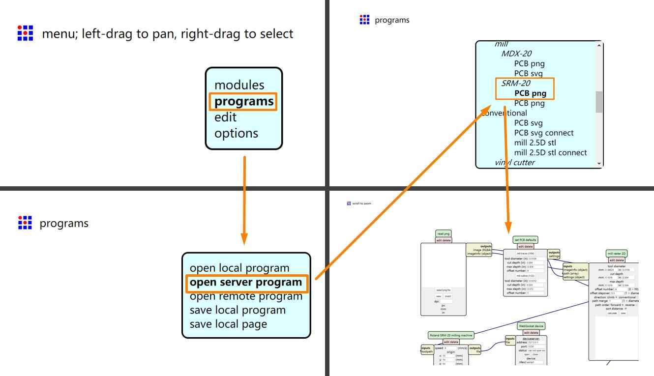
2. Adjust the settings on the mods interface
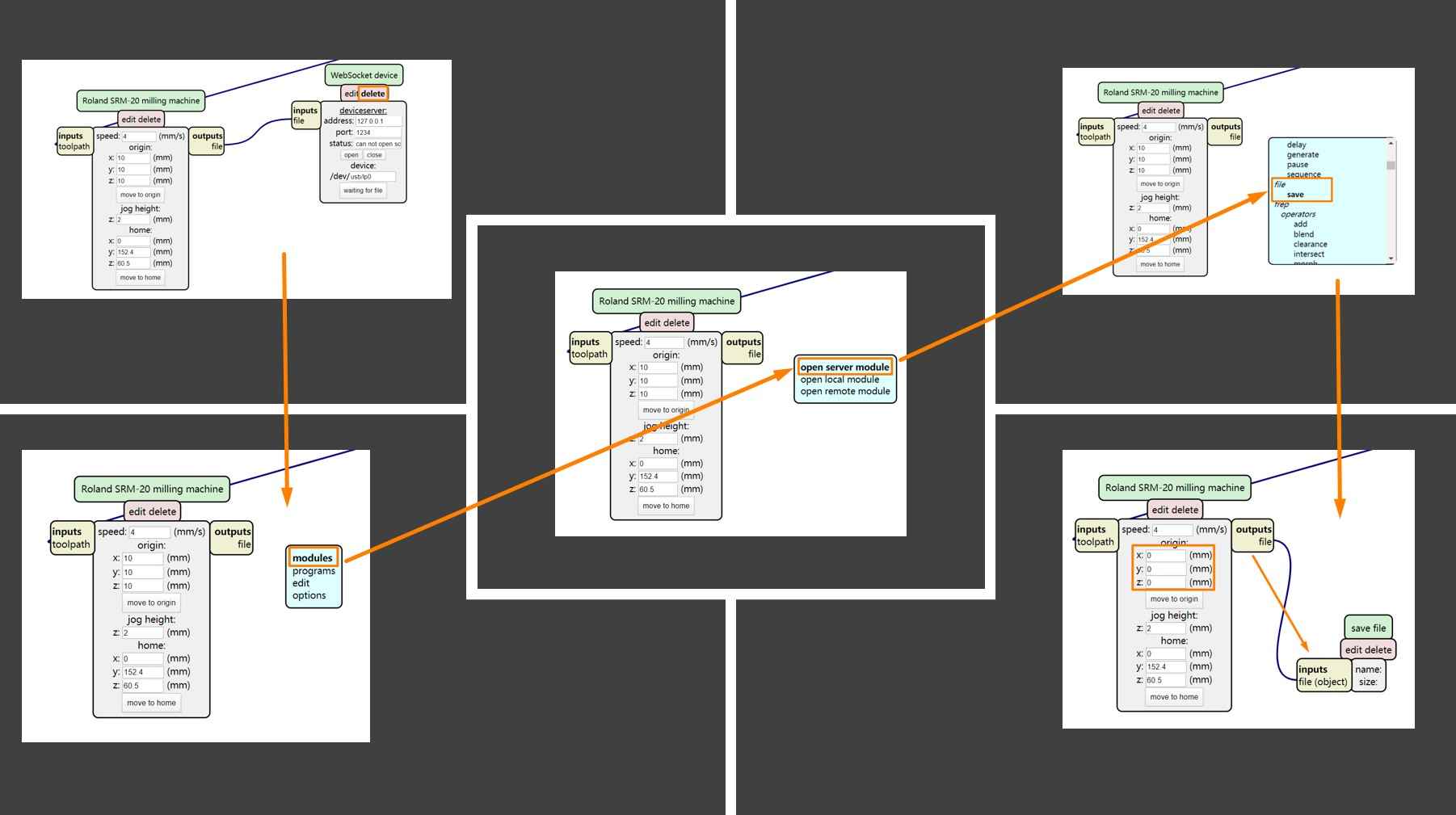
Change file save path by following steps:
Delete "WebSocket Device" module >> Right click >> modules >> open server modules >> file >> save. Then connect the output of Roland SRM-20 milling machine module to the new save module. Also, the origin of x,y,z in the Roland SRM-20 milling machine section should all be set to 0.
3. Process the trace files
Trace Pattern
The trace pattern file defines the actual circuits used for this electronic product, which will be engrave on the PCB board with 0.2 mm - 0.5 mm V milling bit.
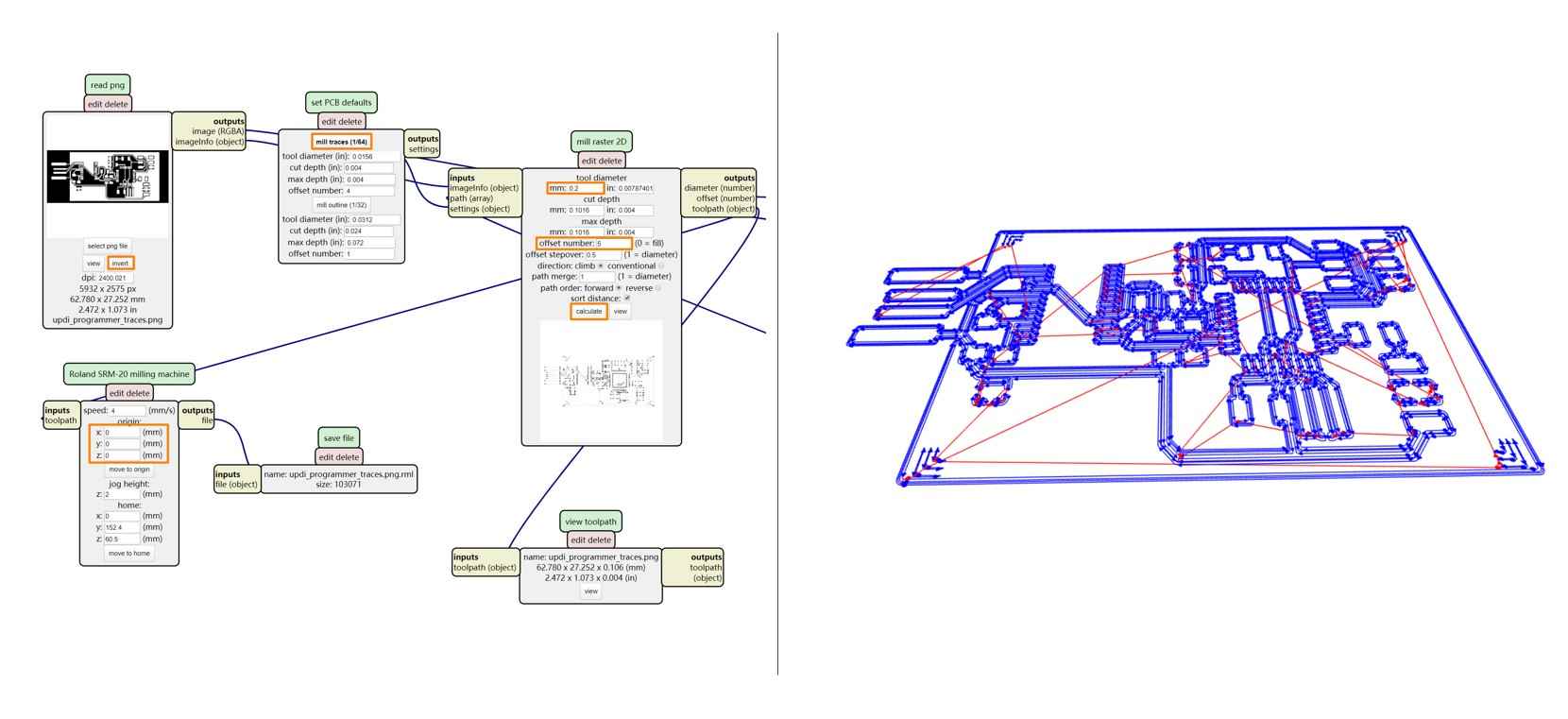
The rml file used for milling can be generated by the following steps:
1. In Read png module, load the file via select png file
2. Invert the file to show the actual trace
3. Set png Default >> mill trace (1/64)
4. mill raster 2D >> tool diameter -> 0.23 mm
5. Set offset number to 5
6. Click Calculate to generate the rml file of trace pattern
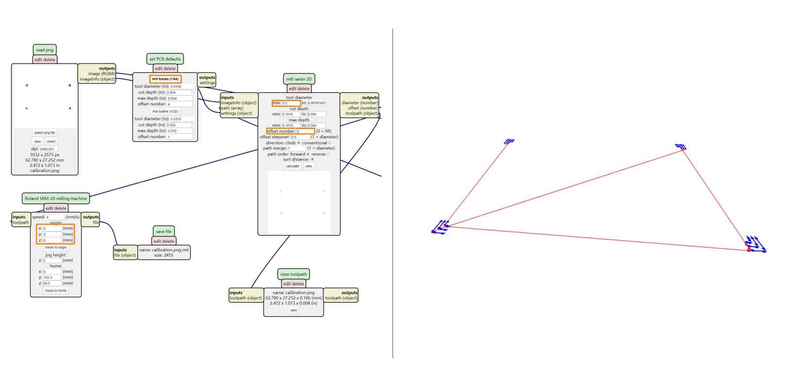
Calibration
For this production, the calibration patterns are several curve lines that locate at the four corners of the trace pattern. The purposes of including these calibration lines are: (1) test whether the milling bit is set with appropriate depth and (2) test whether the board is flat enough for engraving. The procudures are similar to the trace file generation:
1. Load the file in Read png module
2. Maintain the same setting for mill trace and offset number
3. Calculate and save the rml file for calibration pattern.
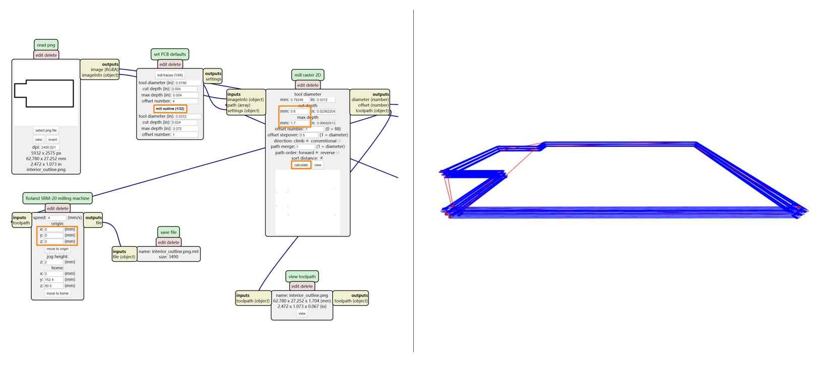
Interior
The interior file defines the outline of the circuit board, which need to be cut through with 1 mm milling bit. Thus, some of the parameters need to be modified.
1. Load the file in Read png module
2. Set png Default >> mill trace (1/32)
3. mill raster 2D >> tool diameter -> 1 mm;
cut depth -> 0.6 mm;
max depth -> 1.7 mm
4.Calculate and save the rml file for interior pattern.
PCB Milling
Machine Setting Up
The first step is to calibrate the milling machine. A Roland SRM-20 milling machine is used for this task. The PCB board and the milling machine need to go through several preparation procedures:
1. Preparing PCB board
A flat and clean PCB board should be used for milling.
● When using an used board, double check if the board has been curved during previous usage. Make sure the back of board is cleaned.
● When using a new board, ensure the photo-resist layer has been removed from the top of the board with iron wool, so the soldering procedure will be easier.
*It is recommended to have this step done in the preparation stage, while it is possible to do this after milling the circuits, especially before soldering if the board has been handled by bare hands.
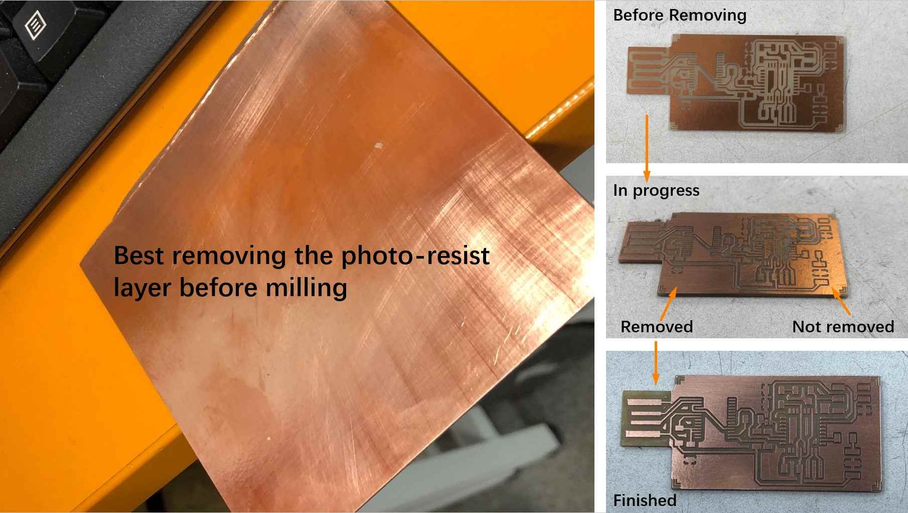
(Left: Process Before Milling; Right: Process After Milling)
● After selecting the proper board and cleaning the milling machine working platform, use double-sided tape to stick the board to the working platform. It is important that the tapes align well and are not overlapping.
2. Install milling bit
To install the milling bit, the operator needs to hold it with one hand and use the hex key tool to fasten it with another hand. The tip of the milling bit is very delicate, which needs to be handled very carefully. If multiple different milling bits will be used for one milling task, each bit need to be calibrate separately.
In this case, a 0.2 mm - 0.5 mm V milling bit is used for engraving the circuit trace and a 1 mm milling bit is used for cutting the contour of the circuit.
Calibration
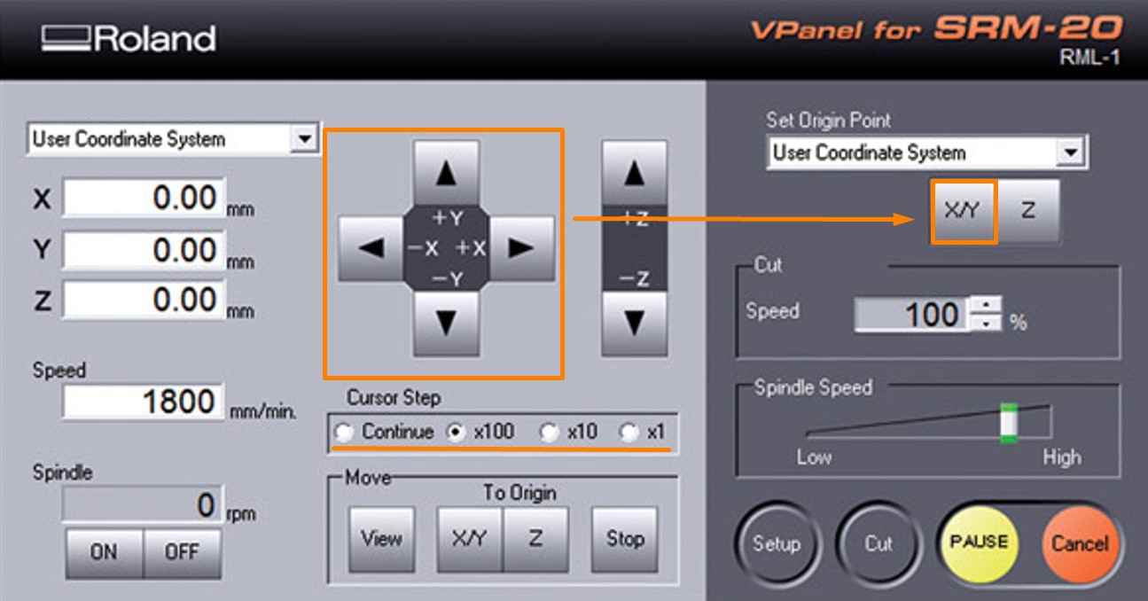
1. Coordination Adjustment
Both the calibration and milling task are accomplished with VPanel for SRM-20 software.
a. Set X/Y origin
The X/Y origin determines the start point on the flat PCB board. The X/Y direction buttons can be used to adjust the X and Y coordination of the milling bit. After reaching the ideal location, click Set Origin Point >> X/Y to set the current coordination as X/Y origin.
b. Adjust Z origin
Z coordination determines the depth of the milling bit.
●Use the Z direction button to lower the milling bit until it is close to the PCB board without touching it. Select a small cursor step when the milling bit comes close to the board.
●Hold the milling bit with one hand and use the hex key tool to gently release it with the other hand. Carefully let the tip of the milling bit touch the surface of the board and fasten it again.
●Click Set Origin Point >> Z to set the current height as the Z origin.
c. Iterative Machine Calibration
For V-shape milling bit, it is necessary to calibrate how deep it cuts into the board. Rise Z for 0.30 mm and set the location as the new Origin Point of Z and test the cut depth with the rml files saved from mods.
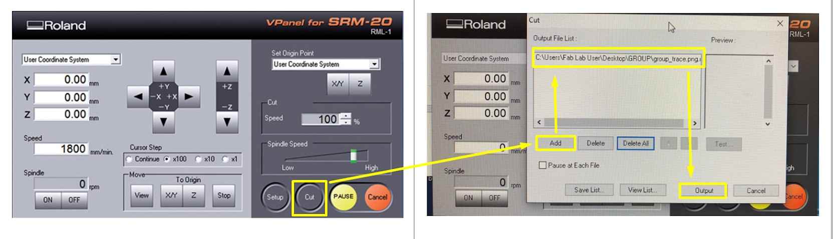
(1) Start the cutting task via Cut >> Add >> Select Calibration.rml >> Output.
*The cutting task will start immediately after clicking “Output”, please double check everything before that.
(2) Pause and Cancel the task if milling bit is not touching the PCB board, which is expected to happen in the early rounds of calibration.
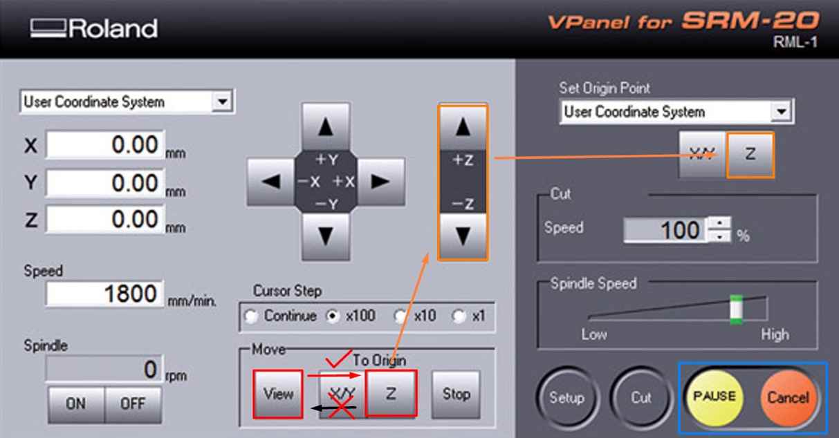
In order to recalibrate, Click View >> To Origin >> Z to bring the milling bit back to its previous position. The order here is very important. Users must click “View” (which will bring the board forward) before clicking “To Origin Z”, otherwise the milling bit may break.
(3)Use the Z direction button to further decrease the height of the milling bit by a small amount and restart the test task. Repeat the routine until the milling bit cuts into the PCB board with appropriate depth. Reset Z origin after adjustment. This depth will be set as the final origin of Z for this milling task.
Circuit Milling
The first step is to engrave the circuit trace to the PCB board.
Then, the 1 mm milling bit is used for cutting the interior of the circuit. After changing the milling bits, the Z coordination needs to be calibrate again. It takes around 30 minutes to accomplish the entire milling task.
Electronic Components Soldering
Components Preparation
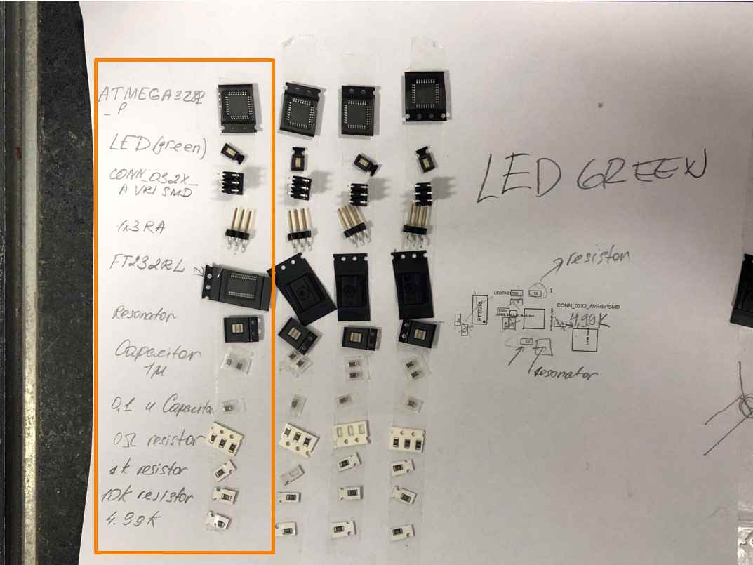
Before soldering, the component that should be soldered on the board should be collected and prepared.
A very efficient way is to use a stripe of double-sided tape to stick all components on a piece of paper, especially when the components are tiny in size.
Soldering
It is highly recommended to follow a Central to Periphery strategy when soldering the components onto the board. In my case, I noticed several noteworthy issues during the soldering process:
1. Check the direction/polarity of components
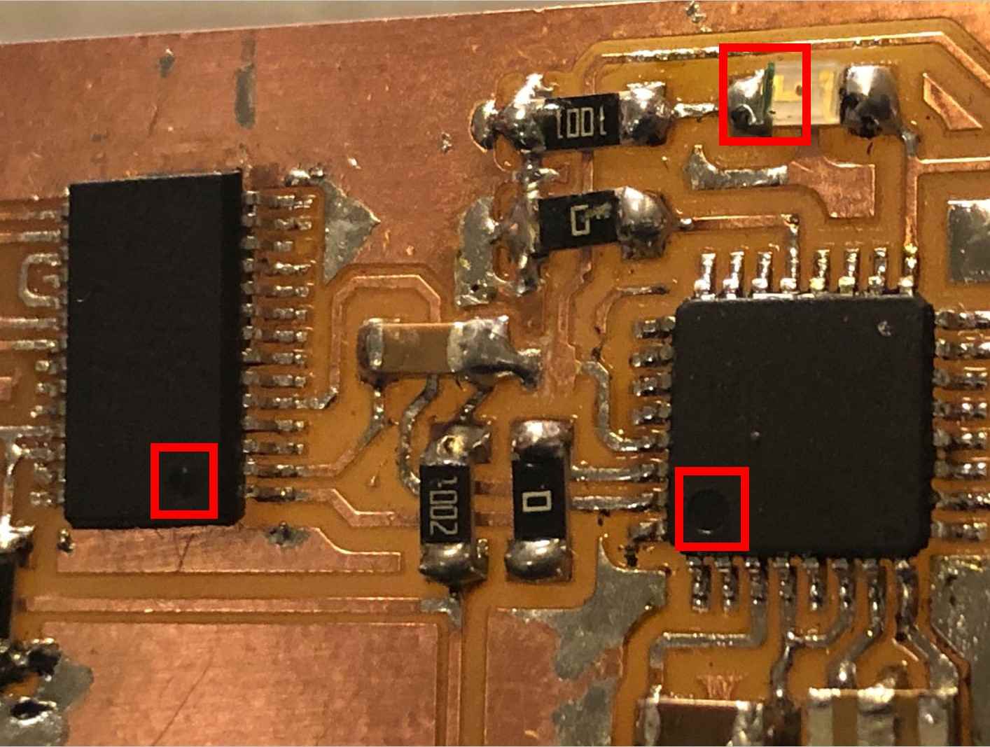
The chips and LEDs, and potentially other components, must be connected with the circuits in certain directions. The direction of chips is usually indicated by the little dot on the top while the polarity of LED is indicated by a narrow stripe of color.
2.Removing the soldered components
Misplaced components can be removed by melting the attached tin with soldering iron or heat guns. Please be extremely careful when removing the soldered components, as it may tear the copper trace from the board and break it.
3. A shortcut to solder chip legs
Instead of soldering the chip legs one by one, it is possible to solder the entire line of chip legs at one time and use the copper tape to remove the extra tin.
4. Test the circuits while soldering
The soldering quality will significantly influence the performance of the circuit, so it may be worthy to frequently test the connection of the circuit and its components with multimeter while soldering the components. In this way, it will be easy to detect the problems and debug.
Programming and Testing
Programming
This board is a updi programmer that utilizes Arduino IDE to program AVR microcontroller.
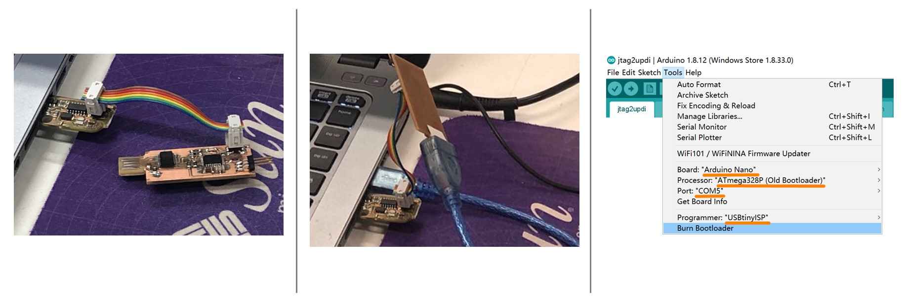
The first step is to program this board, which requires it to be connected to a permanent programmer. Luckily, we do not need to start from the breadboard stage because our instructor Antti has made it for us. At this stage, the procedure is not complicated.The board needs to be connected to both the permanent programmer and the computer, and then the "Blink" code can be used to test if the board have been appropriately connected. If the board is ready to be programmed, the LED on the board should change blink frequencies when the parameter is modified in Arduino IDE.
Burn the Bootloader with the following settings:
Tool >>
Board: "Arduino Nano"
Processor:"ATmega328P (Old Bootleader)"
Port: [The corresponding device]
Programmer:"USBtinyISP"
>> Burn Bootloader
After the board has been program, the circuit path between the FTDI and the ATTiny chips should be cut in order to make the board from an arduino device to a programmer. Skipping this step will induce error in later testing.
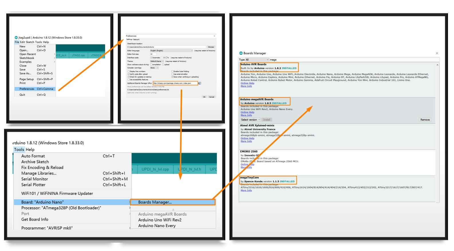
Then, the UPDI sketch should be upload to Arduino. First, download and unpack the files from Github_jtag2updi, which are uploaded into the Arduino IDE. The next step is to install the necessary packages via the following path : File >> Preference >> Additional Board Manager URLs>> Input http://drazzy.com/package_drazzy.com_index.json >> tools >> Boards >> Boards Manager. Then install the megaTinyCore and megaAVR boards packages.
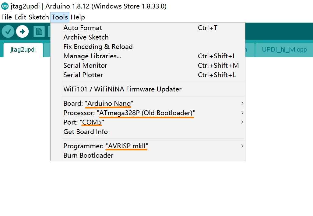
The next step is to upload the jtag2updi files to the board. Connect the board to the computer and upload jtag2updi.ino in Arduino with the following settings:
Tool >>
Board: "Arduino Nano"
Processor:"ATmega328P (Old Bootleader)"
Port: [The corresponding device]
Programmer:"AVRISP mkll"
Top Menu Docker >> Upload
The file seem to be empty, but all the necessary files are linked to it. The IDE will show Done uploading when the task finishes. Now the board works as a updi programmer.
Testing
The effectiveness of the board, which is now a updi programmer, is tested by using it to program another chip, which will enable the new chip to perform simple functions.
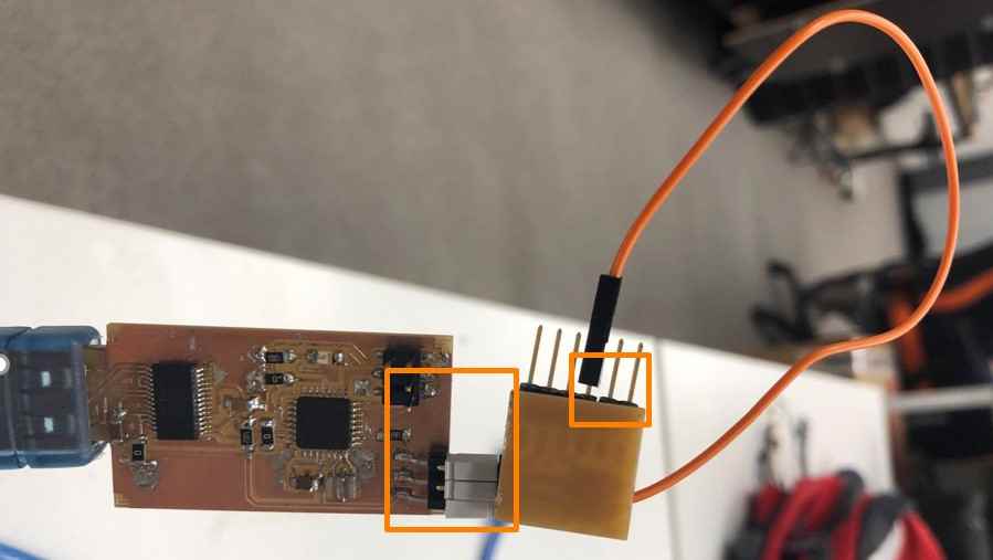
1. Wire the new chip
The first step is to wire the board with the new chip.
 2. Access Arduino file
Open a new file and paste the content of echo.ino into it.
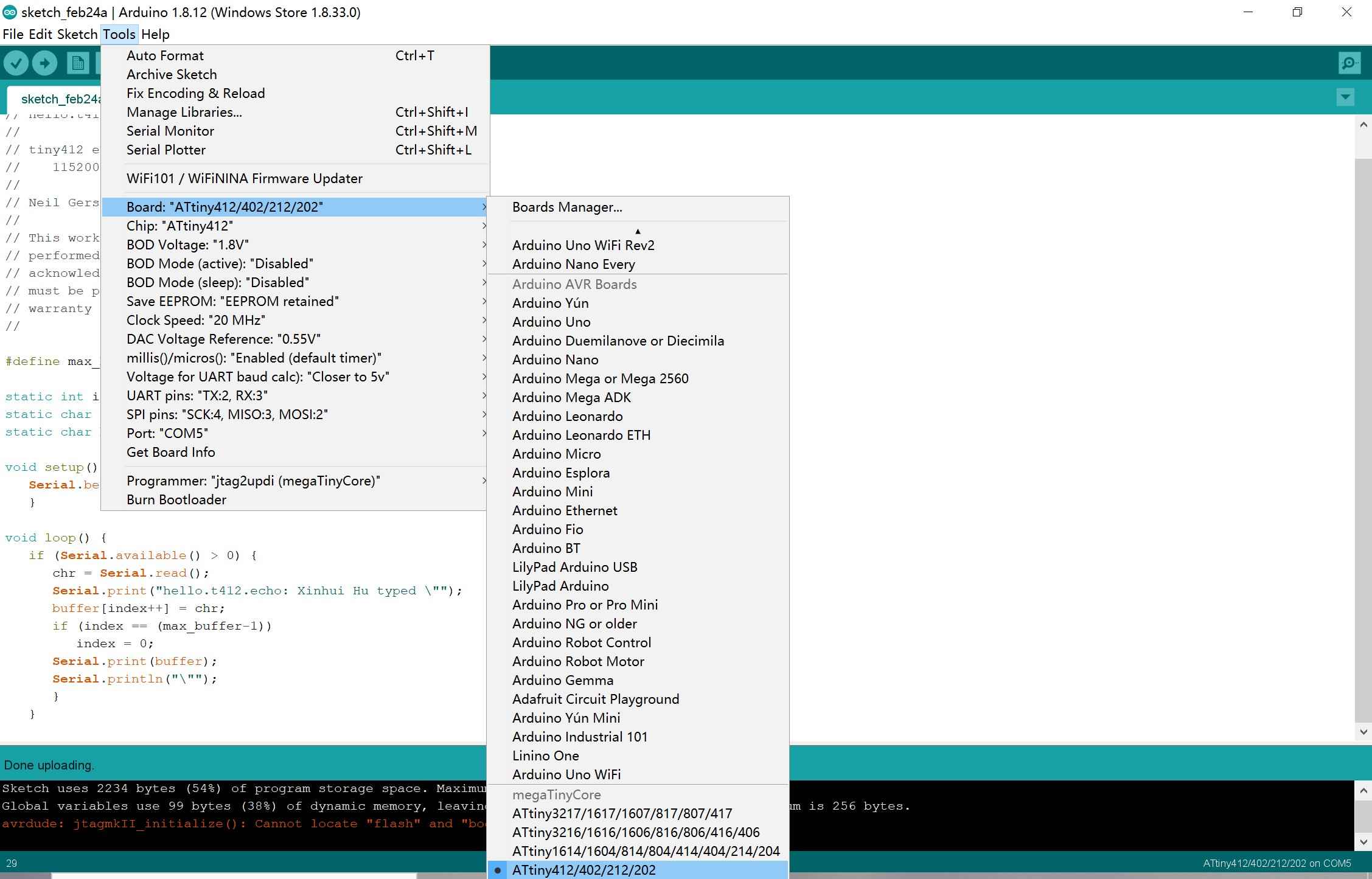
3. Program the chip
Now, the board can program the chip with the following settings and procedures:
Tools>>
Board: "ATtiny412/402/212/202"
...Default Settings...
Port: [The corresponding device]
Programmer:"jtag2updi(megaTinyCore)"
Top Menu Docker >> Upload
The new chip is programmed when the IDE shows Done uploading
 4. Test the new chip
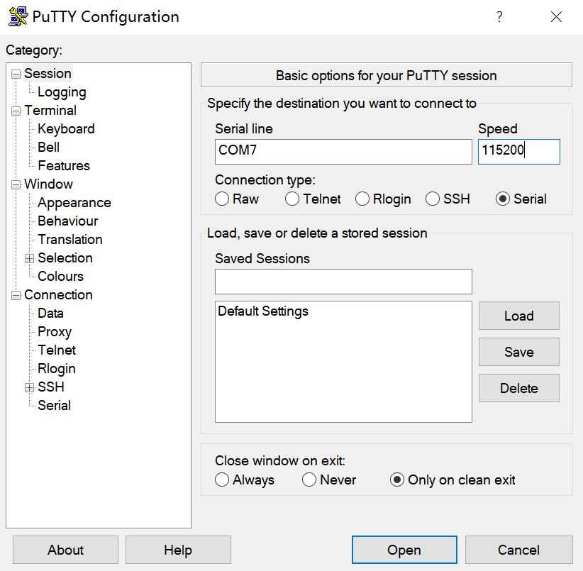
If the board is functioning normally, the new chip should enable the user to achieve simple typing tasks. In order to verify this, the software PuTTY should be installed and used for the test.
After the chip is wired to the computer, adopt the following setting in PuTTY:
Connection type: Serial
Serial Line: [The corresponding device]
Speed: 115200
And then click Open.
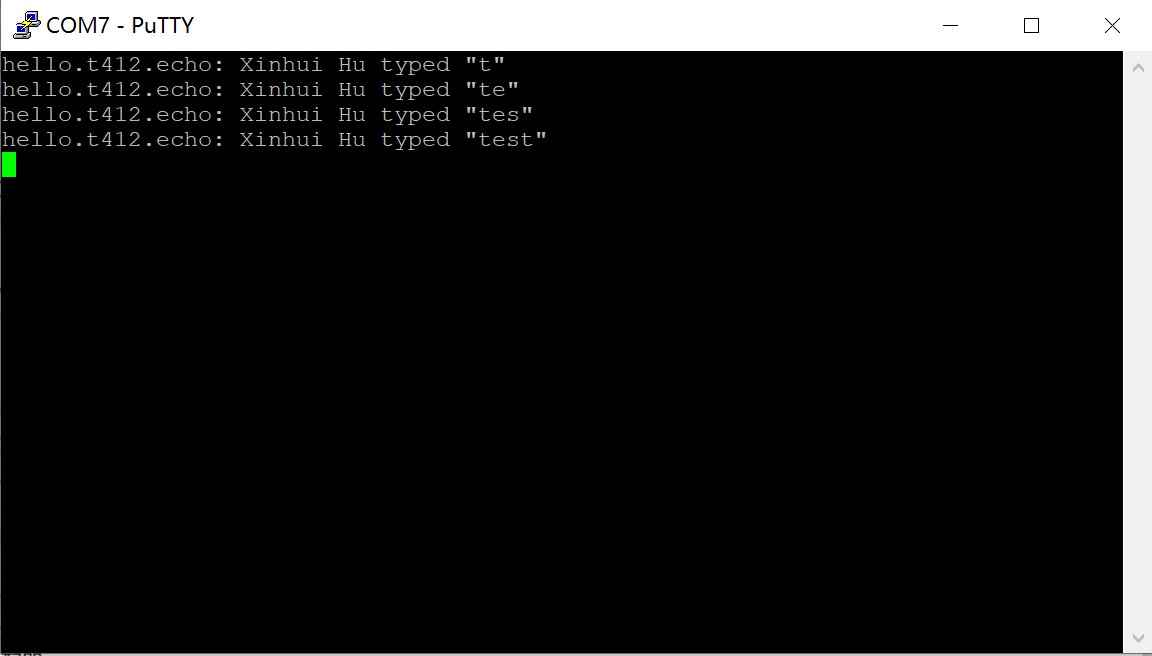
 If the board achieves its function, an interface will pop out, which will record the characters typed by the user.
Files
UPDI pattern pngs:
● Calibration.png
● Trace.png
● Interior.png
UPDI pattern rmls:
● Calibration.rml
● Trace.rml
● Interior.rml